downloadGroupGroupnoun_press release_995423_000000 copyGroupnoun_Feed_96767_000000Group 19noun_pictures_1817522_000000Member company iconResource item iconStore item iconGroup 19Group 19noun_Photo_2085192_000000 Copynoun_presentation_2096081_000000Group 19Group Copy 7noun_webinar_692730_000000Path
Skip to main content
Default Banner Image

inspection

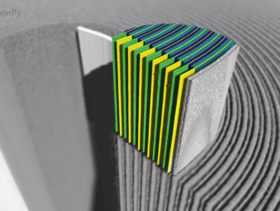
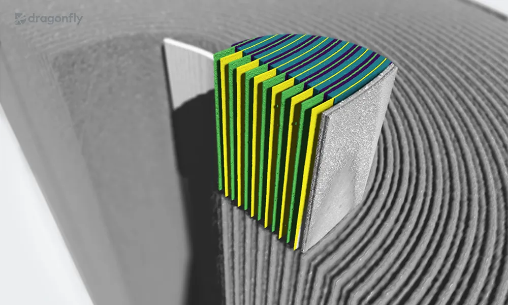
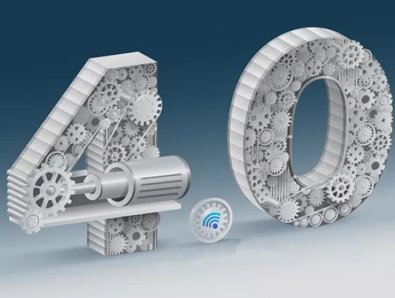
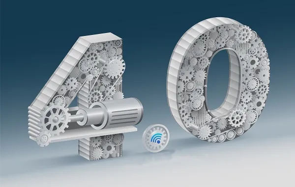
In today’s rapidly evolving semiconductor industry, ensuring both precision and efficiency in manufacturing has become an increasing challenge, particularly as advanced technologies like MEMS and AI chips push the boundaries of design and production. Inspection methods that were once sufficient are now falling short, making room for cutting-edge solutions powered by artificial intelligence (AI). The introduction of AI-driven 3D X-ray inspection technologies is transforming the landscape, offering manufacturers a sophisticated tool to ensure quality control, while driving sustainable production strategies.SEMI spoke with, Joscha Malin, Product Manager, and Daniel Stickler, R D Expert for X-ray Imaging at Comet AG, Industrial X-Ray System Division, to explore how AI-powered 3D X-ray inspection technologies are shaping manufacturing. They delve into how these technologies address critical challenges during inspections and defect analysis, using tools such as Dragonfly 3D World software for user-friendly, AI-driven insights that facilitate effective decision-making.Further insights into the application of AI-powered 3D X-ray inspection technologies and their role in advancing MEMS manufacturing will be presented by Stickler at the SEMI MEMS Imaging Sensors Summit on November 14, 2024, in Munich, Germany. Registration is now open.SEMI: Thank you both for agreeing to share your insights. To start, can you explain the importance of inspection strategies in the context of MEMS manufacturing?Malin: As MEMS devices become increasingly miniaturized and complex, effective inspection strategies are crucial. These strategies not only accelerate the wrap-up of production processes, but also significantly enhance product yield. With tighter tolerances and various materials involved, ensuring the integrity and functionality of each component is more critical than ever. A robust inspection strategy allows us to catch potential defects early, which can save time and costs associated with rework or scrap.Stickler: The evolution of MEMS technology, particularly in AI chips, demands a higher level of inspection sophistication. Traditional methods may fall short in providing the necessary detail and speed, which is why we’re focusing on advanced solutions like our AI-powered 3D X-ray inspection.SEMI: Could you elaborate on how the 3D X-ray technology differs from conventional inspection methods? Stickler: The 3D X-ray technology we utilize acts as a bridge between traditional optical methods and standard 2D X-ray inspection. It offers high-resolution, three-dimensional images without damaging the samples. 3D X-ray technology emphasizes three main benefits: clarity, efficiency, and actionable insights. This means we can obtain detailed images that help us analyze components more effectively, allowing for real-time decision-making.Malin: Moreover, the clarity and detail provided by the 3D X-ray images are critical when it comes to defect analysis in MEMS devices. They allow us to assess mechanical, electrical, and assembly errors in ways that conventional methods simply cannot. This leads to a more reliable production process.SEMI: What specific MEMS defects can be effectively analyzed using this technology?Stickler: There are several types of defects we can analyze. For instance, we can detect mechanical defects such as stiction or fractures, as well as electrical failures like short circuits. The 3D X-ray inspection allows us to visualize these defects in detail. Additionally, we can monitor assembly errors, which are particularly important in complex MEMS devices where misalignments can lead to significant issues.Malin: I’d like to add that early detection of these defects is paramount. The faster we identify issues, the quicker we can implement corrective actions, thereby improving overall yield and reducing production costs.SEMI: You mentioned yield improvement earlier. Can you explain how your technology contributes to that?Malin: Our approach supports process optimization by providing information on product characteristics and, for example, allows us to identify trends early on that may lead to yield issues later. We also aim to accelerate new product introduction in the early phase by rapid feedback, saving time and cost. This is crucial because many defects may not be apparent until later stages of production. With our technology, we can monitor samples in real-time, allowing us to react promptly to emerging challenges.Stickler: By integrating this feedback loop, we can significantly shorten the time to market for new products. This is particularly beneficial in industries where speed and efficiency are essential.SEMI: Can you tell us about Dragonfly 3D World software and its role in this process?Malin: Dragonfly 3D World is a user-friendly software that leverages AI and, specifically, deep learning for image processing. It enables users to efficiently perform bump metrology and defect identification, for example, without needing extensive expertise in the field. The software makes complex processes manageable, even for operators who may not be specialists in image processing.Stickler: Beside MEMS and advanced packaging in GPU production, this software is indeed an “AI-for-AI” application. By utilizing deep learning, users can train models that adapt to various imaging tasks, making the entire inspection process more efficient. The insights generated from the 3D X-ray images are automated, enhancing usability and streamlining workflows.SEMI: In conclusion, what are the key takeaways you’d like to share?Malin: The key takeaways are that AI-driven 3D X-ray inspection is transformative for the MEMS manufacturing process, enhancing inspection strategies and defect detection significantly. By integrating advanced technologies, we can ensure higher product quality and efficiency.Stickler: Yes, and I would emphasize the importance of powerful monitoring and non-destructive test tools. Our innovative solutions not only improve yield, but also pave the way for sustainable practices in manufacturing, ultimately benefiting the industry. Dr. Daniel SticklerDirector X-ray Technology Components at Comet AG, Industrial X-Ray System Division. Based in Hamburg, Germany, he holds a PhD in Physics from the University of Hamburg and has extensive experience in X-ray imaging, semiconductor X-ray applications and product innovations. Joscha MalinDirector Product Marketing Software Products at Comet AG, Industrial X-Ray System Division. Based in Hamburg, Germany, he holds a degree in Electrical Engineering with specialization in Semiconductors and profound experience in the industry. For over a decade, he has focused on developing X-ray inspection and metrology solutions, especially for the Semiconductor industry. SEMI ContactSitong He / Communications Manager, SEMI EuropeEmail: [email protected]: +49 151 5546 2638
Read More
The SEMI Smart Manufacturing Americas Chapter, a key driver of the Global Smart Manufacturing Initiative, accelerates awareness of digital and data-driven strategies and implementations to help speed adoption of smart manufacturing. In 2021, the Chapter will focus on expanding its work across the industry to include academic and research initiatives. The semiconductor industry saw an unprecedented focus on improving digital monitoring of manufacturing activity in 2020, partially due to COVID-19. The Americas Chapter shared case studies on new tools and techniques for social distancing in fabs, aides for remote maintenance, and tips for remote workers. The Chapter also introduced its three pillars of Sensing, Connecting and Predicting and offered related programs. The Global Smart Manufacturing Conference (GSMC) highlighted the significance of universities and research institutions in the development of smart manufacturing with their focus on joint research for broad dissemination. To help drive smart manufacturing advances, at GSMC several offered non-proprietary tutorials on topic including the following: Integrating sensors for acquisition – CEA-Leti Applying new AI and ML tools and strategies to manufacturing – Binghamton University Digital tools for planning, qualifying and management and scheduling in fabs – MINES Saint-Étienne. Adding AI tools to robot work in a smart factory – KAIST Institutes By continuously highlighting the activities of these and other institutions through presentations, interviews, articles and blog posts, we will draw more attention to what is on the horizon for smart manufacturing in 2021. The SEMI Smart Manufacturing Americas Chapter also plans to elevate activities important to the Outsourced Semiconductor Assembly and Test (OSAT), Surface-Mount Technology (SMT) and Printed Circuit Board Assembly (PCBA) segments of the industry including programs on inspection, traceability and the SEMI SMT-ELS Standard for SMT automation. Thurston Taylor, marketing expert at Tokyo Electron and Vice Chair of the Americas Chapter, notes that “With increasingly more demanding requirements for bump, assembly and test, smart manufacturing and applied data science are necessary to achieve back-end goals now and in the future.” Also, many companies are implementing smart manufacturing applications and assessing various strategies to increase their smart manufacturing capabilities. Members of the Americas Chapter plan to review and develop self-assessment documents and maturity models that apply to front-end wafer fabs all the way through packaging and assembly facilities. “Moving forward it is imperative for all of us to up the intensity on specific ROI vectors such as quality, cost, productivity, sustainability and safety leveraging our smart manufacturing SEMI framework of Sensing, Connecting and Predicting,” said noted Bobby Mitra, worldwide director of Smart Manufacturing at Texas Instruments and Americas Chapter Chair. “By offering special flagship events, invited talks, ROI case-studies and ROI criteria in maturity models, we’ll bring high value to the smart manufacturing industry.” Chapter members also will begin mapping the skills needed to implement and support increasingly digital manufacturing capabilities, including any new skill sets, to help companies develop their hiring, training and management strategies. The mapping effort aims to support companies in building a strong pipeline of employees who can efficiently manage and operate smart manufacturing facilities. For its part, the Americas Chapter’s Go Green Subcommittee will focus on applying smart manufacturing technology to reducing the electronic industry’s carbon footprint by accurately tracking energy waste improving overall fab efficiency. Stay tuned for details on activities planned for our chapters in Europe, China, Japan, Korea, Southeast Asia and Taiwan. To learn more about each chapter and how to get involved, please visit the SEMI Smart Manufacturing Hub and sign up for our newsletter. Ayo Kajopaiye is senior project coordinator, Collaborative Technology Platforms, at SEMI.
Read More
The Advanced Lithography TechXPOT at this year’s SEMICON West will explore progress in extreme ultraviolet lithography (EUVL), its economic viability for high-volume manufacturing (HVM) and other lithography solutions that will address the march to 5nm and onward to 3nm.As a prelude to the event, SEMI asked Neeraj Khanna, Global Head of the Patterning Customer Engagement Team at KLA-Tencor, a speaker at the TechXPOT, for insights about the readiness of inspection and metrology tools for EUVL applications at 5nm and 3nm. For a full list of speakers and program agenda, visit http://www.semiconwest.org/programs-catalog/lithography-5nm-and-below.Neeraj Khanna, Global Head of the Patterning Customer Engagement Team at KLA-TencorSEMI: In general, how would you characterize the readiness of inspection and metrology tools intended for EUVL applications at 5nm and 3nm? In particular, what are some of the remaining research and development challenges that need to be addressed for each of these nodes?Neeraj Khanna: KLA-Tencor is working closely with its customers to qualify and ramp EUV. Our suite of inspection, metrology and data analytic solutions are being implemented to enable EUV infrastructure readiness including, for example, new reticle and resist qualification, scanner qualification, and EUV ramp preparation. These EUV integration activities require process control systems that support a wide range of applications, including hotspot discovery, lithography modeling, focus/dose process window qualification, reticle print check, mask blank inspection, and process and tool monitoring.As with any major technology inflection, it is critical to understand sources of process variation to enable ramp at optimal yield. For example, stochastics result in random pattern variations, which have a major impact on EUV yield. To manage stochastics, IC manufacturers are deploying process control solutions that support fast modeling of stochastic variations coupled with high-sensitivity, high-coverage wafer defect inspection. Another example is a methodology called hybrid scanner utilization whereby, when EUV scanners are implemented in production, they will only be used for a few layers, while all other layers will be patterned with 193i scanners. This technique requires tighter control and monitoring of overlay budgets.SEMI: How are you able to achieve this tighter control and monitoring?NK: To understand why hybrid scanner utilization requires tighter control and monitoring of overlay budgets, it’s important to outline how this differs from current scanner implementation. For critical layers in current process flows using 193i lithography, pattern layers for a given wafer are printed using the same stage/chuck on the same scanner. The overlay performance achieved using this lithography strategy is called dedicated chuck overlay (DCO). Use of a dedicated scanner and chuck for lithography reduces inter-scanner and inter-chuck distortion effects, resulting in DCO overlay error of less than 1nm. When EUVL is first implemented in production, it will be used for a few layers – likely, cut masks and contacts with eventual migration to metal 1 layers. All other layers will be patterned with 193i scanners. This hybrid scanner operation eliminates any possibility of using a dedicated scanner and dedicated chuck to support tight overlay performance specifications. Instead, fabs will be forced to optimize mix-and-match overlay (MMO), with the overlay performance obtained using different scanners for printing different layers on a given wafer.With overlay specifications for advanced DRAM and logic at ~2.5nm, fabs will need to implement strict 193i-to-EUV scanner matching strategies or risk consuming 60 to100 percent of the overlay budget on just MMO. To achieve tighter overlay control and monitoring required for MMO, fabs need to implement dense, in-field overlay error measurements that feed into scanner fleet management systems. KLA-Tencor’s ATL™ overlay metrology system supports a high measurement speed and the use of small in-die targets, enabling dense in-field overlay measurements with high accuracy. Our 5D Analyzer® data analytic and management system includes scanner fleet management capability that enables automatic product-based corrections to minimize MMO error, helping fabs reduce the risk to yield loss associated with a 193i-EUV mixed scanner implementation. SEMI: What other challenges do you see coming to the fore at 5nm and 3nm?NK: Overall, the 5nm and beyond design nodes will face challenges associated with new lithography technology, potential new device structures and smaller pattern pitches. IC manufacturers will require process control solutions that not only identify process windows, but also monitor patterning parameters and defectivity at multiple points to identify process shifts. To monitor dynamic processes at these advanced nodes, inspection and metrology tools will need to have both sensitivity to critical parameters/defects and robustness to process variation in order to provide IC engineers with smart feedback for efficient control of their processes.SEMI: Could you elaborate on what will be required to monitor patterning parameters and defectivity at multiple points? How different will the techniques be at 5nm/3nm vs. at say, 7nm or 10nm?NK: As an example of monitoring at multiple points, consider the transition to EUV lithography. With EUV, the cost per scan goes up dramatically. Thus, IC manufacturers will monitor parameters at multiple points to maximize yield and minimize risk: EUV reticle qualification requires inspection and metrology throughout the entire flow from mask blank manufacturing, to the mask shop, to the IC fab. For the advanced design nodes associated with EUV, wafer qualification requires monitoring and control of wafer defectivity, shape and geometry throughout the wafer manufacturing process. It also requires control of fab incoming wafer qualification while ensuring that fab-wide processes are meeting defect and shape standards necessary for printing smaller feature sizes. EUV resist characterization and qualification requires comprehensive lithography simulation, wafer defect inspection, and film thickness and uniformity measurements to help reduce development time and prepare the litho stacks for production ramp. As EUV scanners are ramping, fabs are faced with finding any unknown particle sources within the new scanner chambers. This situation is driving the need for tighter and more frequent PWP (particles per wafer pass) chamber monitors to ensure scanner cleanliness. In addition, EUV scanner qualification requires reticle front and backside particle checks, and hotspot discovery and process window qualification using optical wafer defect inspection and e-beam review. EUV process monitoring encompasses overlay error monitoring, focus/dose monitoring, critical dimension (CD) and 3D device shape monitoring, and continuous process window monitoring. EUV inline defect monitoring and tool monitoring is important for reducing baseline defectivity in the litho cell for faster ramp, and for early identification of litho excursions in production. A critical part of this monitoring strategy is inline after develop inspection (ADI) monitoring, which is defect inspection on patterned wafers after printing and development of the resist ADI. Inline ADI innovations that find yield-critical defects allow fabs to reduce process issues, prevent at-risk wafers early in the process, and enable rework when excursions are found in production. As with past technology transitions, the implementation of multiple monitoring steps as part of a comprehensive process control strategy will be critical for a fab’s successful ramp of EUV.Debra Vogler, SEMI
Read More
New metrology and inspection technologies and new analysis approaches made possible by improving compute technology offer solutions to finding the increasingly subtle variations in materials and subsystems that meet specifications but still cause defects on the wafer. More collaboration across the supply chain is helping too. SEMICON West programs on materials and subsystems will address these issues. New metrology approaches needed to deal with process margin challenges As device process margins shrink and subtler materials variations cause unwanted deviations, the need for better monitoring of both surface and sub-surface material variations is driving a trend towards “metro-spection” – the convergence of metrology and inspection. “Device process margins have eroded to the point that traditional metrology strategies and techniques are no longer viable for controlling yield and parametric performance,” says Nanometrics Vice President Robert Fiordalice, who will speak in the materials program at SEMICON West. “Limited sampling capability, low throughput, insufficient sensitivity or the destructive nature of the techniques can often become problems. What’s more, deviations in material characteristics are not always determined by the initial quality of the material, but often arise from variations during the integration of the materials.” One new type of inline tool or line monitoring technology is Fourier Transform Infrared (FTIR) spectroscopy, traditionally used in quality control or tool characterization. Better sensitivity and higher throughput now enable rapid analysis and feedback for on-the-fly detection of subtle deviations in film properties that may compromise device performance or yield. More advanced analytics will help extract new information from old metrologyMore expensive metrology may not be required to identify subtle variations in in-spec materials that cause wafer defects. Today’s advanced compute capabilities now enable more sophisticated analysis of existing data and the identification of small but significant variations in raw materials and finished goods. The figure of merit (FoM) values presented in certificate of analysis (CoA) reports miss subtle variations in raw material properties. Of particular note is the reduction of molecular weight distributions to a mean, and standard deviation, whereas variations in the tails are associated with pattern defects. Advanced compute capabilities now allow the industry to step beyond the FoM in favor of more holistic measures, enabling predictive analysis of resist chemical variations associated with specific pattern defects. Source: JSR Micro“We often don’t need to find a new measure, but just a new way of looking at what we measure now,” says Jim Mulready, vice president of global quality assurance at JSR Micro. Mulready will speak in the SEMICON West program on materials defectivity issues. “The certificate of analysis reduces multiple measurements to a single figure of merit. But if we ignore all that raw data, we miss a chance to learn. One of our sayings in quality is ‘Customers don’t feel the average, they feel the variation.’ In many electronic materials, the quality of the raw material can have a big impact on the final performance, but the types of analysis needed to look at the tails of the distribution of these measures (such as molecular weight) in detail used to be really hard to do. Now it’s becoming increasingly straightforward and affordable.” Mulready says tools now available in the data processing sector enable the identification of subtle variations in materials that can cause defects on the wafer. These tools use methods like detailed subtractions of chromatography curves of polymer raw materials or analysis of tails of distributions of molecular weights. “Our job now is to drive these kinds of more sophisticated data analysis back into our chemical supply chain as well,” says Mulready. “We must work more closely with our suppliers to integrate their raw materials into our products. The reason the JSRs of the world exist is as a safety valve to reduce the variation from the chemical industry before it gets to the fab.”Continued collaboration with equipment suppliers required While the industry has been talking about the need for tighter collaboration between materials suppliers and equipment manufacturers for years, it still doesn’t always happen. “The material supplier and the equipment maker are tied together like kids in a three-legged race when we deliver an integrated system for consistent on-wafer performance,” says Cristina Chu, TEL/NEXX director of strategic business development, another speaker in the materials program. “When we introduce changes to the tool hardware, we need to make sure it doesn’t upset the system. Similarly, we need the material supplier to send a bottle over when a new chemistry formulation is under development. If a new chemistry runs into problems in the field, it will take much more time for both of us to fix it at the customer site. The toolmaker can provide a slightly different perspective on applications, while being more objective than a customer on how the formulation performs compared to earlier versions.”Regular and ongoing collaboration between chemistry suppliers and toolmakers enables the highest quality system solution to reach the customer. Chu notes that her team tries to maintain consistent collaborations with material suppliers across changes in organizations as the business environment changes. “For consistent on-wafer capabilities, we need a consistent collaboration process with chemistry suppliers. We need to meet with materials providers at a regular cadence throughout their development process. We need to check back with them as we scale up results from the coupon to the wafer level and to work out the kinks in the integrated solution together. The quality and consistency of our combined performance at the customer depends on ensuring the quality and consistency of our development and evaluation process as well.”Fabs and subsystems suppliers look to pilot data sharing program to improve process margins With ever tighter process margins, subtle variations in parameters that don’t appear in the specifications are also compromising results on the wafer, and neither the fab nor the supplier alone has the full information needed to improve performance. To help, a SEMI standards group is developing a protocol for a pilot program to standardize and automate some data sharing.The fab knows that performance is best with a particular parameter value, and knows when performance fluctuates, but often faces a black box problem with no way of knowing what exactly is wrong. In the rush to get the tool back up, the fab engineers may not get around to emailing the supplier about the issue for some time. The subsystems supplier, on the other hand, may know the cause of the variation, but likely has no way of knowing the critical parameters or ideal target values for the fab’s process. “In order for engineers to have constructive conversations about how to improve performance, we all need to exchange more information,” says Eric Bruce, Samsung Austin diffusion engineer, and co-chair of the SEMI Standards initiative addressing the issue, who will speak in the subsystems program at SEMICON West. A potential solution could be to create a standard and automated process to share particular data, agreed to in the purchasing contract, whereby the subsystems supplier shares more information about their parameters with the fab, and the fab in return gives feedback on what parameters work best to drive improved performance. The best place to start will likely be on parts that do not contain core yield-related IP, but where usage and lifetime information is useful.“We’re looking for people to participate in a pilot program to work together with suppliers to try sharing some information to improve performance,” says Bruce. “There’s a lot of this sharing in the backroom anyway, but this could make it fast and automated, and make everyone’s engineering job a lot easier.”Paula Doe, SEMI
Read More
The Scaling Technologies TechXPOT at this year’s SEMICON West (Scaling Every Which Way! – Thursday, July 12, 2:00pm-4:00pm) will explore traditional scaling as the industry marches toward 3nm and beyond, as well as technologies that enable 3D architectures, die stacking, and interconnect scaling. The session will also provide an update on how the various players (foundry, IDM, fabless, and application developers) are jockeying for innovation leadership. As a prelude to the event, SEMI asked Priya Mukundhan, director, Technology Development and Applications, at Rudolph Technologies, and a speaker at the TechXPOT, to provide her insights into challenges associated with metrology and inspection.For a full list of speakers and program agenda, visit http://www.semiconwest.org/programs-catalog/scaling-every-which-way. Priya Mukundhan, director, Technology Development and Applications, Rudolph TechnologiesSEMI: What are the key challenges that need to be addressed to provide the kind of metrology and inspection solutions that will be needed by the industry as scaling – in all its forms (e.g., traditional, 3D ICs, interconnect, and different transistor architectures) – is pursued at 5nm and then at 3nm? Priya Mukundhan: With respect to metrology needed to scale FinFETs, the following will be key: Gate critical dimension (CD) at the fin sidewall, gate height, gate profile Fin CD, height and profile Dopant profiles Stress measurement in the fin Composition in thin film and interface These challenges are currently being handled using in-line CD solutions, CD scanning electron microscopy (CD-SEM) and CD atomic force microscopy (CD-AFM), along with optical critical dimension (OCD) measurements. There is no single technology that can take all of these measurements, and determining the right solution is application-dependent[1].Issues associated with inspection and scaling include the following: Bright-field inspection lacks the sensitivity to detect defects smaller than those found at the 20nm node Detecting defects that are 5nm or smaller is achieved using electron beam inspection tools, but these single-electron beam inspection systems are prohibitively slow and cannot meet the high-volume manufacturing (HVM) requirements for defect inspection Buried defects Void detection in 3D SiP structures, front and backside inspection Sidewall crack detection in packaging SEMI: Can you provide a summary of the R D roadmap for metrology/inspection tools that you see emerging in order to get to 3nm? PM: Hybrid metrology is currently in use, especially for CD metrology. To support the development efforts, techniques that provide complementary information as well as those that eliminate uncertainties will be required. Researchers at imec[2] have started exploring technology combinations to gain insight into how new structures function. Some of the findings in imec’s study include the following: The combination of transmission electron microscopy (TEM) and scanning probe microscopy (SPM) provides a unique approach of imaging combined with a functional analysis capability In situ SPM could potentially determine composition (SIMS) as well as functional properties (electrical) Fast Fourier transform scanning spreading resistance microscopy (FFT-SSRM) is a novel technique that measures carrier profiles in semiconductors. This overcomes the current SSRM limitations of signal distortions due to parasitic resistances while measuring on small volumes such as FinFET and nanowires Multi-electron beam inspection can be used for HVM for sensitivity to smaller SEMI: How will metrology and inspection be impacted beyond 3nm? What kinds of tools will be needed by that point in time?PM: There are several different transistor options that have been identified by leading edge wafer fabs and consortia looking beyond the 5nm node roadmap[3,4]. Some of the options on the table include the following: 1) Extension of the current FinFET in the form of gate-all-around FET2) Creating them with new materials by adding ferroelectrics (e.g., negative capacitance FET, or NC-FET) 3) Complementary FET4) Vertical nanowires and nanosheet FETsThese possibilities bring new challenges and require characterization at the material level. Also, the industry as a whole will have to redefine what it means to do composition at the nanometer level. This could be the beginning of a trend towards array-based metrology, i.e., measurements on an array of devices to gather statistically significant data[2].Regarding metrology needs at 3nm, it is too early to determine what kind of tools would be needed only for R D and how many of them would need to be extended to high-volume manufacturing (HVM). From an inspection perspective, there will be a continued migration towards computer aided design (CAD)-based inspection, as well as having the ability to deal with large image data sets (petabyte, big data). Furthermore, inspection algorithms should be improved, along with better staging for better image stitching.References Bunday, E. Solecky, A. Vaid, A. F. Bello, X. Dai, “Metrology capabilities and needs for 7nm and 5nm logic nodes,” Proc. Of SPIE, Vol. 10145, 101450G, pp. 1-41, 2017. Imec roadmap and imec magazine. Intel roadmap. https://semiengineering.com/transistor-options-beyond-3nm/ Debra Vogler, SEMI
Read More