downloadGroupGroupnoun_press release_995423_000000 copyGroupnoun_Feed_96767_000000Group 19noun_pictures_1817522_000000Member company iconResource item iconStore item iconGroup 19Group 19noun_Photo_2085192_000000 Copynoun_presentation_2096081_000000Group 19Group Copy 7noun_webinar_692730_000000Path
Skip to main content
Default Banner Image

wearables

As healthcare undergoes a digital transformation, semiconductor technologies are emerging as a critical foundational enabler, making care more personalized, proactive, and accessible. At SEMI, we’re proud to highlight the leadership of STMicroelectronics (ST), a member and active participant in our Smart MedTech initiative’s governing council, for their commitment to advancing this critical frontier.With decades of experience in sensing, power management, and connectivity, ST is helping to shape a future where electronic systems seamlessly integrate with healthcare and wellness solutions, empowering both patients and providers.The Rise of Wearables and the Role of SemiconductorsST has long delivered innovation in automotive, industrial, and consumer electronics. Now, the company is applying its expertise to wearable health technologies, a rapidly growing segment that’s reshaping how we monitor, diagnose, and manage health.Today’s wearables go far beyond their predecessors. They capture vital signs and biomarkers such as heart rate variability, ECG signals, blood pressure trends, and more with medical-grade accuracy, providing real-time insights that can inform treatment and improve outcomes. This evolution represents not just a technological leap, but a shift in how we deliver and think about healthcare.A Shared Mission to Scale MedTech InnovationST’s active engagement with SEMI’s Smart MedTech initiative reflects our shared commitment to building an agile, responsive ecosystem that can bring life-changing technologies to the market faster. Through Smart MedTech, SEMI unites leaders across the electronics and healthcare value chains to identify systemic barriers, spark cross-sector dialogue, and co-create strategies for scalable success.ST brings invaluable perspective and technical depth to this mission. Their approach focusing on full solutions rather than standalone components, demonstrates how semiconductor companies can play a central role in enabling integrated healthcare systems.Meeting the Moment: Prevention, Personalization, and ReachHealthcare systems globally face mounting challenges: aging populations, chronic disease burdens, rising costs, and a projected shortfall of 18 million healthcare workers (WHO, 2019). Against this backdrop, wearables and remote health monitoring tools are poised to deliver tremendous value.As ST points out, the economic case is clear: treating chronic disease can be 100 times more expensive than prevention, wearables offer a proactive path forward. By enabling continuous, at-home health tracking, these devices empower individuals to take control of their wellness and allow providers to intervene earlier and more effectively.Accelerating the Future TogetherAt the SEMI 2025 Technology Workshop, ST joined a panel discussion exploring how semiconductors are reshaping healthcare. The session highlighted the need for earlier diagnosis, personalized care, and scalable solutions amid rising chronic disease and healthcare labor shortages.Panelists emphasized moving beyond component sales to integrated, system-level solutions. ST’s role on the Smart MedTech governing council emphasizes their commitment to cross-sector collaboration and advancing MedTech adoption.The MedTech revolution requires more than great products, it demands aligned ecosystems, shared knowledge, and coordinated strategies. As a member of SEMI and a key voice in our Smart MedTech initiative, ST exemplifies how semiconductor innovation can drive real change in healthcare.We’re proud to work alongside ST and other industry leaders who are committed to creating smarter, more sustainable healthcare through electronics. Because in today’s healthcare landscape, an ounce of prevention enabled by semiconductors isn’t just worth a pound of cure, it’s a blueprint for global health resilience.See the full ST article STMicroelectronics and Medtech: Enabling Personalized Healthcare and Wellness through the Integration of Electronics featured on Smart MedTech webpage.Gity Samadi is Senior Director of R D at SEMI.Rafael Tudela Senior Technical Marketing Manager at SEMI.Michelle Smith-Moritz is Senior Program Manager, Smart MedTech at SEMI.
Read More
New treatments for vascular disease. Optimized agricultural production. Beefed up performance of wearable devices and flexible displays. Four students with their sights set on making the world a better place won Innovators of the Future awards at the 20th Annual FLEX Conference in late February after presenting novel ideas for advancing flexible electronics in the popular student poster event. It was clear that all of these young innovators are working on projects with the potential to impact our lives in the near future. Their work is critical to advancing products, devices and basic research in flexible electronics. Posters created by the 17 students who competed for the awards were judged by a multidisciplinary panel of industry experts. The posters reflected a broad range of applications enabled by flexible hybrid devices and covered technology for wearables, medical devices and precision agriculture. Innovators of the Future Award Winners Robert Herbert from the Georgia Institute of Technology won first place for his paper Smart and Connected Stent System with Nanomembrane Soft Sensors for Wireless Monitoring of Hemodynamics. Vascular diseases are the leading cause of death worldwide, accounting for over 30% of all fatalities. Early diagnosis and monitoring blood pressure and flow rates are critical to effective treatment. Herbert’s poster introduced a less costly, less invasive and more revealing (spoiler alert) sensor system that uses a flexible, wireless biosensor system with an inductive medical stent and capacitive pressure sensors. The laser-machined stent uses multi-layered material integration to function as an inductive coil for wireless communication while maintaining mechanical properties similar to conventional vascular stents. The stent and sensor system can be easily deployed using conventional catheter procedures. Watch his presentation. Jose Waimin from Purdue University’s School of Materials Engineering was one of two second-place winners for his poster that shows how real-time monitoring of ion concentration, moisture, pH, microbial activity and other key metrics in agricultural production can optimize crop yields while reducing environmental impacts. His work presented a scalable alternative for manufacturing low-cost flexible sensors that can be used in an array of applications. Electrodes are manufactured in a Roll-to-Roll (R2R) process to enables fast production at a very low cost per device. Watch his talk. Benham Garakani from Binghamton University, Center for Advanced Microelectronics Manufacturing (CAMM) was the other second-place winner for his paper Electromechanical Behavior of Flexible Silver Paste and Highly Stretchable Liquid Metal for Wearable Electronics. Garakani explored how to improve fabrication of reliable, comfortable wearable devices to boost performance and functionality using substrates such as nonwoven high-density polyethylene fibers (HDPE) and thermoplastic polyurethane (TPU). Garakani also examined the electromechanical reliability of screen-printed silver trace on HDPE fibers and stencil-printed liquid metal (Ga-In-Sn alloy) on TPU during isothermal fatigue cycling. Watch his presentation. Sridhar Sivapurapu from the Georgia Institute of Technology won third place for his poster Flexible and Ultra-Thin 30µm Glass Substrates for RF and mmWave Flex Applications. Sivapurapu’s poster addressed the increasing demand for maximizing the mechanical flexibility of flexible displays while maintaining or improving their electrical performance. Sivapurapu focused on both electrical and mechanical properties for determining the viability of ultra-thin glass stack-ups for flexible RF applications by benchmarking the electrical performance of the ultra-thin glass stack-up to 110 GHz. He also examined electrical characterization during bending tests using free arc bending. Watch his talk. The Innovators of the Future award was sponsored by FlexEnable, a technology provider that develops flexible organic electronics technologies and OTFT materials. All FLEX Conference 2021 presentations are available through March 26, 2021 by registering for the event. Gity Samadi is co-chair of the FLEX Conference student poster awards and program manager at SEMI FlexTech.
Read More
Tracking and quickly diagnosing COVID-19 infections, working from home and telemedicine recently came into sharp focus as technology executives and other subject matter experts from microelectronics heavyweights recently gathered for the first-ever virtual SEMI CTO Forum to explore how the microelectronics industry and their own companies can leverage future technology trends to drive growth. Themed Intelligent Medtech and Wearable Technologies, the forum drew CTOs from ARM, Babblelabs, Brewer Science, Dell, Dow/Dupont, E-Ink, Hewlett Packard Enterprise, Intel, Lam Research, KLA, Microchip, ON Semiconductor, Qualcomm, Tokyo Electron, Ulvac, Veeco and Xilinx. The event is designed as a strategic driver of pre-competitive innovation. Following are key takeaways from the forum. Microfluidics Promises to Speed COVID-19 Diagnosis More than 240 companies worldwide are developing microfluidics solutions to improve diagnosis and treatment of COVID-19 and other conditions, said forum speaker Dr. Kurt Petersen, a member of Band of Angels, Silicon Valley's oldest angel investment group, with an illustrious background1 in technology. And their innovations are bearing fruit. Cepheid, a company founded by Dr. Petersen, has developed a disposable microfluidic cartridge, Xpert Xpress SARS-CoV-2, used by doctors to swab the inside of a patient’s mouth. Highlighting the vital role of MEMS in medical electronics, the tiny powerful devices are behind a test that can detect COVID-19 infection in under 40 minutes. Dr. Petersen also cited a few examples of implantables and injectables under development, including: In vivo chemical sensing: Profusa developed a continuous glucose monitoring sensor via an optical patch. Glaucoma pressure monitors: Injectsense built a silicon chip the size of a grain of rice that is embedded in the eye to measure eye pressure. Retinal implants: Second Sight implanted a 60-electrode array chip that projects images onto the retina to improve vision. Microelectronics Takes Aim at Battling COVID-19 The event’s CTO roundtable, a platform for discussing societal and technology issues, revealed microelectronics technology will likely give rise to solutions for combatting pandemics and new business opportunities both in the short and long run. Areas of the greatest interest included: Tracking and Security: Infection tracking accuracy is key to limiting the spread of viruses yet comes with inherent privacy and security challenges. The consensus view of the executives was that developing trusted hardware capabilities is critical for adoption of accurate infection-tracking technologies. Remote Operation: Executives expect working from home or the use of telehealth to continue building momentum long after pandemic. To give staying power to the remote communications at the heart of these trends, microelectronics ecosystems will need to boost compute performance, both at the edge and in the cloud, while increasing bandwidth to enable applications such as augmented reality/virtual reality (AR/VR), artificial intelligence (AI), machine learning and advanced data analytics. Edge intelligence: The challenge of remote communications spans both people and the Internet of Things (IoT). Questions persist about how hundreds of billions of sensors will connect to the cloud and how much power they will consume. The need to push computing to where data is generated – at the edge – is rising and the necessary underlying technologies will only come by combining various forms of distributed computing and analytics. The microelectronics industry’s ability to seize these opportunities will only be possible with huge strides in innovation, raising concerns among the CTOs about the financial viability of cutting-edge devices because of increasing device complexity and R D costs. Technology partnerships and collaborations – an area where SEMI is contributing and will continue to expand its efforts as it works with the CTO community – will be critical to containing R D costs. SEMI will help the executives identify and mobilize the resources key to future innovation. Improving Home, Work Productivity and Experiences Key to AR Adoption Smart wearables also offer great promise. In just over a decade, AR and VR have grown from science fiction to practical uses such as AR applications for smart contact lenses, said Dr. Mike Wiemer, Co-Founder and CTO of Mojo Vision2. Dr. Wiemer said that while many AR applications remain under development, the technology will only see widespread adoption once it starts to improve productivity and efficiency at home and work and the quality of other experiences. The smart augmented reality contact lens developed by Mojo Vision is a step in that direction. The product’s built-in display gives users timely information about everything they see while remaining invisible by packing 70,000 pixels into a space smaller than a half a millimeter across, making it the smallest and densest dynamic display ever made. The contact lens is powered by an ARM-based processor, with later versions adding an image sensor, eye-tracking sensors and a communications chip. SEMI thanks EMD Performance Materials and Telit for sponsoring the CTO Forum. For more information on the CTO Forum and SEMI’s Smart Data-AI initiative, please sign up on our webpage. 1 Dr. Kurt Petersen is a member of the National Academy of Engineering, an IEEE Medal of Honor winner, and a Life Fellow of the IEEE for his contributions to the commercialization of MEMS technology. 2 Dr. Wiemer also co-founded Solar Junction, where he led technical teams to two world records in solar cell efficiency (43.5% and 44%). He also has patents and papers in Semiconductor Devices Applications, Silicon Photonics, Materials Integration, Lasers, Solar Cells, Solar Systems, and Analog Circuits. Tom Salmon is Vice President of Collaborative Technology Platforms at SEMI. Pushkar P. Apte, Ph.D., is Strategic Technology Advisor for the Smart Data AI Initiative at SEMI.
Read More
Since 2015, FlexTech has funded three projects with ITN Energy Systems, based in Littleton, Colorado. The projects all draw on a unique concept of using thin, flexible ceramic sheets as both a substrate for functional devices and as an integral part of the hermetic packaging to support paper-thin FHE products. Each program was increasingly sophisticated, enabling a larger variety of functions to be integrated into a common package. Independent functions such as energy storage, energy harvesting, or printed microelectronic circuits are deposited on their own ceramic substrate and the layers vertically stacked and interconnected into a monolithic structure that combines several functions in the smallest possible package volume.The ITN projects provide excellent examples of the power of collaborative research and development to help de-risk investments in next-generation electronics. All the projects were conducted with technical contributions from small and large businesses as well as university partners. The programs were funded by the U.S. Army Research Laboratories (ARL), directed by industry leaders and managed by SEMI FlexTech with the focus on utilizing the advantages of flexible hybrid and printed electronics (FHE) to create lighter-weight, lower-power, more conformable electronics than available commercially today. Markets ready to take advantage of FHE developments include healthcare, aerospace, mobility, consumer electronics, industrial electronics.ITN was founded in 1995 to focus on researching and developing technologies related to aerospace, energy and the environment for defense and commercial marketplaces. Its business model employs collaborative R D projects to explore, develop and validate promising next-generation clean energy technologies with an emphasis on tackling the manufacturing challenges that enable low-cost, high-volume production of thin-film devices on flexible substrates. Those technologies that meet the technical and business requirements of the market are commercialized via focused, spin-out companies with five such spin-outs formed so far. The work on ultra-thin batteries needed by the SEMI FlexTech community readily slid into their portfolio of projects.Project 1 – New Solid-State Lithium BatteryThe first project kicked off in 2016, with ENrG, and successfully supported the development and validation of novel Solid-State Lithium Battery (SSLB) products with total packaged thickness ranging from 50-250 microns. The SSLB proved to have substantial advantages in form factor and performance when compared with both commercial-off-the-shelf batteries and emerging technologies. For example, the SSLB provided more than double the operating time in a substantially smaller package in powering an audio device supplied by SEMI FlexTech partner companies.By avoiding the use of liquid electrolytes, the ITN SSLB also eliminates flammability issues while still allowing the benefits of lithium-based battery chemistry. The SSLB boasted many attributes attractive to the FlexTech community, including: Ultra-thin form factor, i.e. 250 microns thick, mAh class packaged batteries High volumetric energy density, i.e. baseline products with ~500 Wh/l and a roadmap to 1,000Wh/l The ability to support high current pulsing, i.e. current pulses at 4-10C rates, in support of demanding FHE duty cycles High temperature compatibility with solder reflow and other FHE integration schemes Rechargeability with high capacity retention at 1,000 cycles This new SSLB has formed the foundation of subsequent projects and commercialization efforts.Project 2 – Adding Energy Harvesting Based Recharging Capability The second SEMI FlexTech-funded project proposed a novel self-recharging battery with the addition of Lucintech’s cadmium telluride (CdTe) photovoltaics (PV), which was also deposited on thin yttria stabilized zirconia (YSZ) substrates. Because the CdTe supports a superstrate configuration, the SSLB can function as the back sheet for the PV package, thereby dramatically decreasing overall package thickness. The resulting flexible integrated power pack provided up to 0.25 Wh of energy storage and ~0.2 W of PV generating capacity in a total package less than 250 microns.As part of that effort, the ITN Team identified an effective power-management circuit that was ultimately compatible with die thinning and form factors very attractive to FHE. Consequently, the PV and SSLB were interconnected into a common power bus that enabled FHE to be operated with either the PV, SSLB or some combination of the two.ITN is seeing great interest in this product and both developing a version with substantially higher capacities than the project entertained for a UAV platform while ramping to low volume with support from NextFlex, a member of the Manufacturing USA network, and formed in 2015 through a cooperative agreement between the U.S. Department of Defense (DoD) and FlexTech Alliance.Monolithic integration of function layers atop of SSLB for high performance microelectronics device Project 3 – Integration with Processing and Sensor SystemsThe third FlexTech-funded project builds further on that foundation. In this project, the ITN Team is maturing the technologies to create a battery with an integrated processing and sensor system, nicknamed BiPASS. In addition to SSLB layers, the BiPASS package integrates printed circuits on YSZ employing high-performance, silicon- based bare die micro-electronics and/or thin film sensors into the common packaging. Mock-up of the charge control circuit on SSLB The initial demonstration integrates a commercial lithium battery charge control circuit within the SSLB packaging to create a monolithically integrated power module. There have also been promising developments of the University of Rhode Island’s metal oxide (MOx)-based thin film gas sensors that have dramatically increased sensitivity when deposited on thin YSZ. The resultant sensor achieves ppb detection of trace explosives gases that can be powered by SSLB. Along the way, ITN’s partners Molex and SunRay Scientific matured several aspects of FHE circuit printing and integration on both PET and YSZ, including new materials and processes for conductive traces, and bare die attachment with fine features. The project is in its final stages and the ITN Team now has a promising roadmap to integrate power, microelectronics, and thin film sensors/sensor systems into a single paper-thin package.Commercial Scale-Up StrategySince the initial demonstrations were completed, ITN has been actively maturing a commercial scale-up strategy based on significant market-pull and interest from several companies. A new venture to commercialize this next generation SSLB is in process. As part of those discussions, ITN is in active discussions with potential strategic partners to support the transition to high-volume production to access additional markets, many of which are cost-sensitive and need a higher degree of production maturity.In the meantime, ITN’s limited volume SSLB production line is already supporting medical device customers. In addition, a baseline SSLB (~2.5 mAh capacity) has been developed and tested in several new applications, including wearables, sensors and smart labels.“Based on the acceptance of these project in the market, I believe all three projects have provided significant value to the SEMI FlexTech community,” noted Brian Berland, Chief Technology Officer at ITN. “In addition, the connections and visibility we have gained within the industry by partnering with SEMI FlexTech have been invaluable. We are excited to continue this journey with new and additional projects. In the meantime, we are hopeful that our ongoing discussions with investment partners will support our commercializing of these components.”For more information visit www.flextech.org. SEMI FlexTech is currently (from 6/10/2020 – 7/17/2020) accepting white papers for new technology development projects. Read more at www.flextech.org.About the AuthorDr. Gity Samadi is the SEMI FlexTech Program Manager. Gity is responsible for the flexible hybrid electronics R D consortium activities including project awards and management, Technical Advisory Council management, and webinar/industry event planning for the building and fostering of this dynamic innovative community.
Read More
A multidisciplinary team of researchers is developing new methods to collect and analyze sweat for clues about how the body is functioning.Imagine if you could know the status of any molecule in your body without needing to get your blood drawn. Science fiction? Almost – but researchers at the University of Arizona are working on ways to do this by measuring molecules in sweat.When physicians take blood samples from patients, they send the samples to labs to be analyzed for biomarkers. These biological clues indicate everything from cholesterol levels to disease risks, and they can be used to monitor patient health or make diagnostic decisions. The same biomarkers also are found in sweat.Using $519,000 in funding from SEMI-NBMC (Nano-Bio Materials Consortium), Erin Ratcliff, University of Arizona materials science and engineering professor and head of the UArizona Laboratory for Interface Science of Printable Electronic Materials, is leading a project to develop new ways of collecting and analyzing the clues sweat has to offer. Ultimately, this work could allow physicians to use patient sweat samples in the same way they currently use blood samples, for a less invasive and more informative approach to establishing and monitoring patient health.“What’s unique about this is that we are combining biology and engineering expertise to develop a wearable device that will detect molecules in sweat, so you don’t have to get your blood drawn to know the health status of your immune system, your nervous system, indeed, any system in the body,” said co-investigator and sweat biomarker pioneer, Esther Sternberg, MD. “The goal, eventually, is to create a device that will provide physicians and health care providers the ability to monitor your health status continuously and in real-time without needing to draw blood.” Materials science and engineering professor Dr. Erin Ratcliff in her laboratory at the BIO5 Institute at the University of Arizona “We are pleased to sponsor and eager to complete this project with University of Arizona’s impressive team bridging the disciplines of engineering and life sciences,” notes Melissa Grupen-Shemansky, PhD, Chief Technology Officer and Executive Director of SEMI-NBMC. “A concerted interdisciplinary approach at the early stages of R D is relatively new and there is much learning on both sides. The UA team brings unique strengths in both areas and we are excited to be partnering and collaborating with them.”Ratcliff’s co-investigators are J. Ray Runyon, a research assistant professor in the Department of Environmental Science, and Sternberg, research director for the Andrew Weil Center for Integrative Medicine; director of the Institute on Place, Wellbeing, and Performance; and the Andrew Weil Inaugural Chair for Research in Integrative Medicine. Ratcliff and Sternberg are both members of the BIO5 Institute.Standardized Sample CollectionIn order to study sweat, researchers need to collect samples of it, and there are a number of ways to do so.“The obvious idea would be to make a patch that gets information from many pores at once, but the problem is that this creates a space between the patch and your skin, and you have to wait for it to fill up with sweat,” Ratcliff said. “We hypothesize that while you’re waiting, these molecules – the very molecules you’re trying to detect and analyze – are changing chemically.”The team’s first task is to develop new, continuous and hands-free collection devices that deliver high-quality, standardized sweat samples. This will allow health care professionals to gain a more holistic picture of a patient's bodily systems over an extended period, rather than the “snapshot” a blood draw can provide of a particular moment.Currently, sweat labs across the world are using different methods to collect samples, which limits researchers’ ability to compare data. Standardizing the collection method could provide researchers, including medical device developers, with a new degree of confidence in sweat sample data.“High-quality data, with respect to different target molecular biomarkers in sweat, requires that a high-quality sample be collected,” Runyon said. “This will be the first hands-free method that will truly take into account the interplay of the chemistry of sweat, the target biomarker and the device material.” University of Arizona student in classroom testing medtech devices Low-Level DetectionThe team is also developing methods for researchers to detect and analyze neuropeptides in the collected samples. Used by neurons to communicate with each other, these small molecules are involved in biological functions, including metabolism, reproduction and memory. Commercial wearable devices monitor metrics like heart rate, and some use sweat sensors to monitor dehydration level. Measuring neuropeptides, however, will allow researchers to zoom in millions of times closer to investigate stress and relaxation responses at the molecular level.“The idea is that your sweat is reflecting your nervous system – all of the neurotransmitters your body uses to signal between the brain and the rest of the body,” Ratcliff said. “Monitoring this biochemical response continually, over a 24-hour cycle, can inform us about the health of the wearer and also act as a diagnostic tool.”Meet Dr. Ratcliff and the University of Arizona team at FLEX in San Jose, Calif., February 23-26, 2020. Emily Dieckman is Editor at The University of Arizona. Republished with permission from the University of Arizona.
Read More
MEMS technology has changed human interaction with electronic devices. Introduced in the 1990s, the first mass-market MEMS devices were used for inkjet printheads and automotive airbag crash sensors. Today, MEMS are ubiquitous, with billions of the tiny devices adding intelligence and interactivity to smartphones, smart speakers, wearables, automobiles, biomedical devices, remote monitoring and event detection systems, and countless other applications. Integrating MEMS with Flexible Hybrid Electronics (FHE) is an important step in the evolution of this miniaturized intelligent sensing technology, paving the way for its use in new classes of flexible, conformal devices.The integration of the two technologies promises to breed new applications in small form factors but also presents challenges inherent to FHE design and fabrication processes. SEMI’s Nishita Rao caught up with Nathan Pretorius, prototyping and automation engineer, NextFlex, to discuss MEMS-FHE device integration challenges and opportunities ahead of his February 26 presentation, Integrating MEMS Devices in FHE, at FLEX|MEMS Sensors Technical Congress (MSTC) 2020, February 24-27, 2020, at the DoubleTree by Hilton in San Jose, California.Join us at FLEX|MSTC to meet Nathan and other industry influencers advancing innovation in FHE and MEMS sensors. Register now to connect with him at FLEX|MSTC or visit him on LinkedIn.SEMI: Why is integrating MEMS devices into FHE systems important? What new use cases might it enable?Pretorius: The main value proposition of integrating MEMS devices into FHE is that it allows MEMS devices to exist in a different form factor than was possible previously, giving us high-quality MEMS sensors on the flexible and conformable platform of FHE.Ease of application, flexibility, lower cost and rapid iteration on a design are just some of the benefits of FHE devices. And because there are few robust FHE sensors that overlap with MEMS’ capabilities, when you combine the two, you get a lot of compelling uses. That’s why NextFlex is working with agencies and companies to evaluate MEMS’ integration, including using bare MEMS die with microfluidics and promoting new ways of attaching and packaging MEMS die for use with FHE. SEMI: Why is FHE an ideal platform for integrating various types of sensors?Pretorius: MEMS integrated with FHE devices are ideal for rapid design and deployment of data-gathering sensor nodes — which we can iterate for specific applications. A few examples include on-body health monitoring devices for bio-fluids analysis, medical pressure sensors for monitoring blood pressure, and peel-and-stick sensors nodes for infrastructure monitoring. In terms of design and production, FHE devices support rapid prototyping, allowing for instantaneous design-iteration cycles. This speeds design-to-production over traditional rigid PCBs and copper flex because the feedback cycle time between design, manufacturing and testing is shorter, accelerating time to market. What’s exciting about FHE technology is that a variety of sensors or components, including MEMS, can be designed into the base system to easily customize it for a specific application. In addition, our experience shows that when compared to a traditional rigid PCB, an FHE board reduces manufacturing steps and device weight by two-thirds and, perhaps most importantly, converts the device to a thin, conformal shape that makes possible products in new form factors. SEMI: What are the primary challenges to integrating MEMS with FHE? What is NextFlex doing to help device manufacturers address these challenges? Pretorius: There are a few challenges, some of which are device-specific. Most recently, I’ve been focusing on inertial and timing devices, including accelerometers, gyroscopes and resonators. There are a few technical challenges involved in the process of getting the devices from the wafer to an FHE substrate. The wafer processing is very important, especially the dicing and thinning steps. After thinning and dicing, the die is placed onto the FHE substrate. The stresses caused by bonding to the substrate have to be understood and characterized. After placing the die, you then have a calibration step, which is normally performed after the device is packaged. With a MEMS die placed onto directly onto an FHE substrate, calibration then must be done.Finally, the device encapsulation is important, since on an FHE substrate the hard-to-soft material transition is very important to mitigate stresses to rigid component interfaces. We have also been looking at how to work with devices that have damping vents. Flexible encapsulants are inherently more permeable to gases and water vapor than hard encapsulants, so studying the encapsulation of MEMS devices on FHE is another area of interest. NextFlex has been working in a supporting role to evaluate best design practices and best attach and integration methods. In addition to our ongoing collaborative programs, NextFlex is developing the FHE manufacturing ecosystem to include system and component manufacturers and designers, product developers, and materials and equipment providers.SEMI: How do we facilitate closer collaboration between the FHE manufacturing ecosystem and MEMS suppliers such as MEMS device manufacturers, product developers, and materials and equipment providers?Pretorius: It’s important to include manufacturers early in the design process so we can identify challenges up front. That’s why NextFlex spearheads technology road-mapping efforts that include representatives from across the manufacturing ecosystem. We use the roadmaps to prioritize challenges that we can address effectively through collaboration, focusing the industry on solving problems through Project Calls that reveal integration challenges and results from real devices and that tell us how the materials and equipment actually perform with a real device.NextFlex keeps the information flowing, holding quarterly project update webinars to share results. As current devices are optimized for the process in which they will be used, we learn a lot from the project performers who make FHE system demonstrators — and we share that information with the member community. SEMI: Can you point to an example of a successful MEMS-FHE device integration?Pretorius: MEMS-FHE integration is still in the early stages, but we are working on several projects including a DARPA Seedling project for which we have integrated MEMS sensors into FHE systems for testing and evaluation. We plan to continue this work by integrating MEMS and FHE devices using methods that support mass production.SEMI: What would you like FLEX|MSTC attendees to take away from your presentation?Pretorius: We would like to see the FHE community work more closely with MEMS device manufacturers. For example, NextFlex often works with manufacturers to gain access to bare die, which is still a significant hurdle in making devices.The best way to speed things along is to get involved. We encourage FLEX|MSTC attendees to join NextFlex. As a prototyping and automation engineer at NextFlex, Nathan Pretorius explores new print methods for prototyping and automation using novel materials and processes. Pretorius currently focuses on how best to apply software scripting and machine learning to streamline FHE processes. Prior to joining NextFlex, he researched the strengths of roll to roll and screen printing on printed electronics designs, including capacitive touch interfaces, FHE passive component design, and antennas. Nathan holds a Bachelor of Science degree in Graphic Communications from Clemson University. FLEX|MSTC is organized MEMS Sensors Industry Group (MSIG) and FlexTech, SEMI technology communities focused on the growth of MEMS sensors and the flexible electronics supply chain, respectively.Nishita Rao is marketing manager for technology communities at SEMI.
Read More
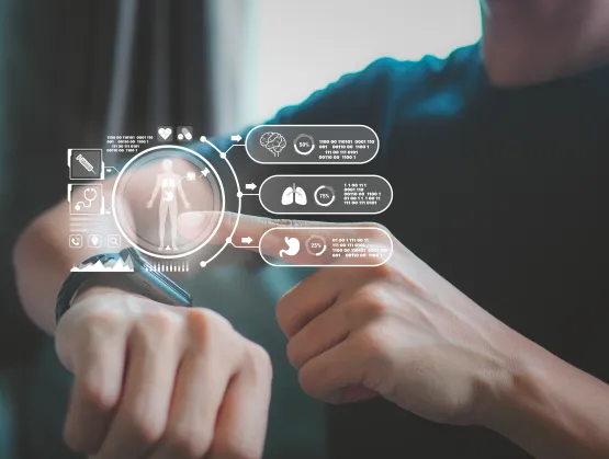
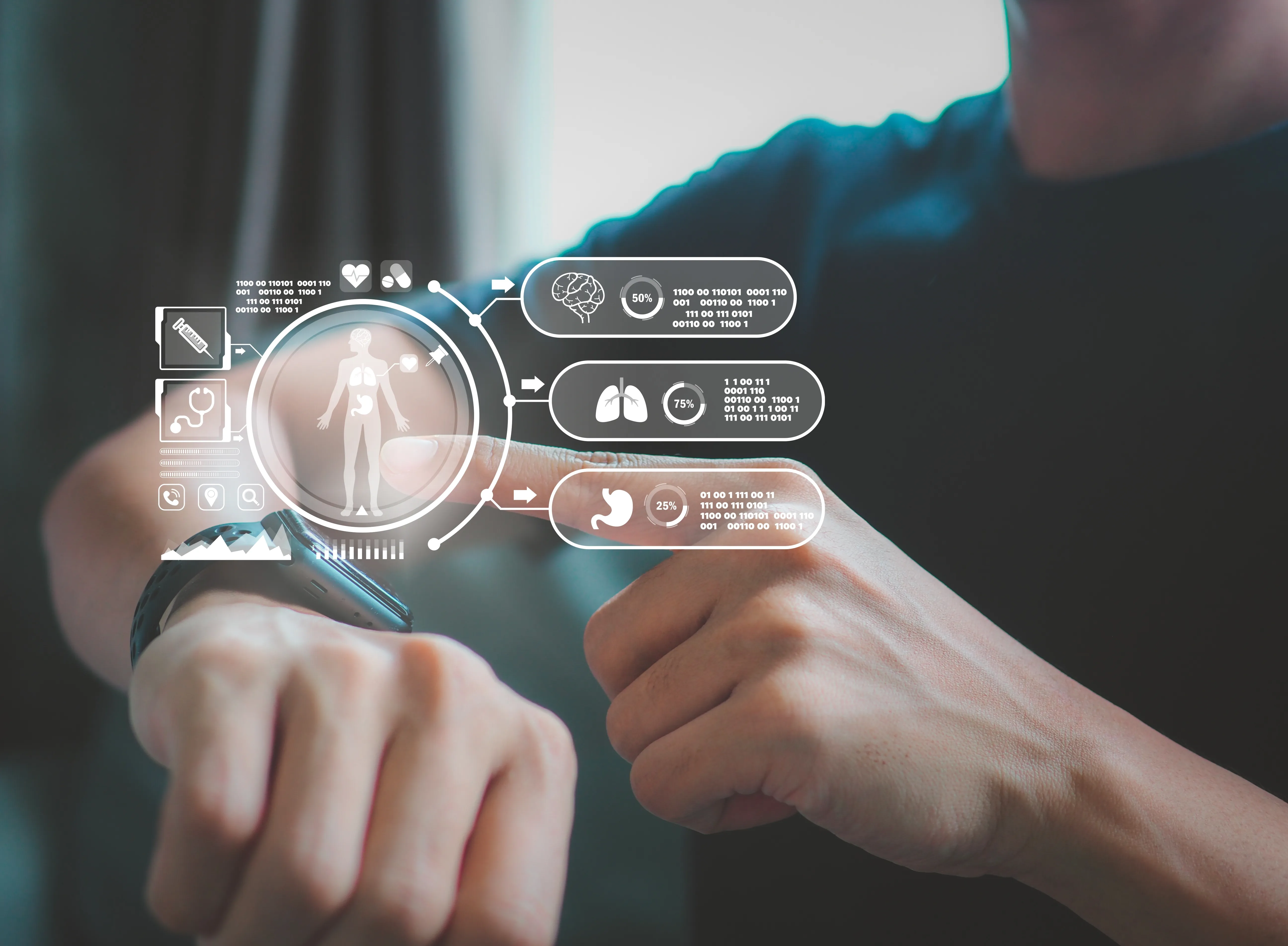
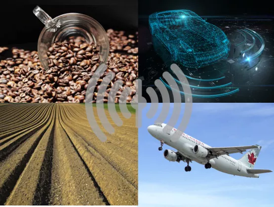
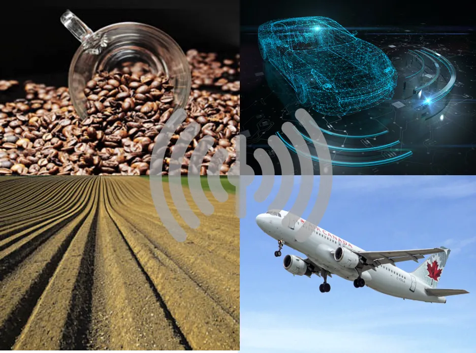
Part of 1 of 2-part series on MSEC 2019 highlights. Read Part 2. MEMS and sensors are proliferating across consumer, automotive, biomedical/healthcare, robotics, industrial and agriculture applications to harvest sensory data in a hyper-connected world and meet demand from consumers and organizations alike as they clamor for more intelligence in electronics.Take the ubiquitous iPhone. Shipped in 2007, Apple’s first iPhone sported five sensors. By contrast, the most feature-packed smartphones will embed up to 20 sensors by 2021, according to Yole Développement’s Jérôme Azémar. He estimates that the devices will feature four MEMS microphones, four CMOS image sensors (CIS), a RGB color sensor, a laser rangefinder, an infrared sensor, a gas sensor, a heart rate monitor and a fingerprint sensor, not to mention the MEMS inertial sensors that device users have come to know and trust.The MEMS market is expected to reach $18.5 billion in 2024 [1], up a whopping 60 percent from $11.6 billion in 2018, according to Azémar, who presented at MEMS Sensors Industry Group’s 15th annual MEMS Sensors Executive Congress (MSEC) in late October in Coronado, Calif. Add other types of sensors to the mix – CIS, environmental sensors, LiDARs, radars, ultrasonics, and fingerprint sensors – and the market will mushroom to $93 billion by 2024, said Azémar.Since MEMS Sensors Industry Group (MSIG) joined SEMI as a Strategic Association Partner three years ago, SEMI has expanded its MEMS and sensors programs to Europe and Asia while continuing to grow its U.S. conferences. “SEMI is continually investing in MEMS and sensors innovation across the supply chain,” said Dave Anderson, president of SEMI Americas and host of MSEC. “For example, MSIG is contributing to the development of the Heterogeneous Integration Roadmap, an initiative designed to drive heterogeneous integration technology development and accelerate electronics innovation. The roadmap spans device design, test and fabrication, ecosystem development, R D, equipment and materials. “At MSEC, executives and other speakers explored how AI and blockchain are remaking the food supply chain, air transportation and other sectors as MEMS and sensors improve the quality of our lives,” said Anderson.Sensing at the EdgeThe concept of artificial intelligence (AI), that a machine can harness intelligence that rivals or outperforms humans – and act without human intervention – has been a feature of the human imagination since at least the 1968 film 2001: A Space Odyssey. MEMS and sensors facilitate intelligence in a wide range of electronics such as smartphones, healthcare wearables, robots, industrial predictive maintenance systems, and cars. AI is sure to augment that functionality.MEMS and sensors are now in their third wave of evolution, a focus on edge AI, Bosch Sensortec CEO and General Manager Stefan Finkbeiner told MSEC attendees. For its part, Bosch is working to add AI to MEMS devices. The first wave integrated software with MEMS sensors, and the second, sensor fusion, enabled designers to allocate performance and power strategically to tune MEMS for resource-constrained devices. The third wave is “an active-learning phase in which MEMS facilitates real-time learning at the edge to promote greater personalization, environmental feedback, privacy of user data and improved battery life,” said Finkbeiner.Small sensor nodes with edge AI exemplify third-wave applications. Integrating low-power environmental sensors (e.g., gas, temperature, pressure, humidity and air-flow sensors), the nodes could be deployed in fire-prone forests to assess fire risk and support early detection. Access to this real-time environmental information could prove invaluable to residents and public-safety personnel alike.Google takes another tack, applying machine learning to resource-constrained devices, said Nick Kreeger, a senior software engineer at the Internet giant. The company’s Google Brain creates machine learning models that can run on inexpensive, low-power microcontrollers using Google’s TensorFlow Lite, an open-source machine learning tool that’s been deployed on a multitude of mobile devices. Inferencing is done at the device’s edge, rather than transmitted to the cloud.Meeting the power constraints of battery-powered sensing devices is another matter that starts with minimizing energy and data waste. “Deep learning is compute-bound and runs well on existing microcontrollers,” Kreeger said. “Because it’s all arithmetic, it’s low-power compared to storage access.”Already Google has worked with Plant Village, a research unit at Penn State University, and the International Institute of Tropical Agriculture (IITA) to help farmers improve food production by using machine learning and cheap sensors to spot and manage planet diseases in developing countries. And that production chain is in dire need of a boost, according to Rajendra Rao, general manager of IBM Food Trust, an enterprise-class blockchain solution.“We are on the cusp of complete failure of the food system,” Rao said. “One out of 10 people gets sick each year from foodborne illness, 420,000 die from this annually, 80 percent of companies in the food supply chain have not digitized, one-third of all fresh food in the US is thrown away, and one in five seafood samples worldwide is mislabeled.”IBM Food Trust’s work with Sucafina, which manages a global green coffee supply chain, shows how sensors can trace food from the farm to the processing plant to the consumer. With the IBM Food Trust platform, Sucafina can track the origin of the beans used in a cup of coffee – a competitive differentiator to coffee drinkers eager to support fair-trade coffee roasters.ripe.io, one of Forbes’ 25 most innovative AgTech startups, is also tackling the challenges and complexities of the food supply chain.“Our secure blockchain platform creates a digital twin of food items, transparently aggregating foods’ journey in real-time, to provide a harmonized trustworthy platform for multiple stakeholders,” said Rachel Gabato, the company’s COO. The ripe.io blockchain-based platform collects data from various sensors – temperature, pressure, light, humidity and inertial MEMS sensors. Growers, distributors and end customers including sweetgreen – a U.S. restaurant chain that depends on fresh produce – use the information to trace the origin and quality of food.MSEC 2020Mark your calendar for next year’s MSEC, October 12-14, at Coronado Island Marriott Resort Spa in Coronado, Calif. Get updates from MSIG on MSEC and other upcoming events including MSTC 2020.Stay in Touch with MSIGMEMS Sensors Industry Group (MSIG), a SEMI Strategic Association Partner, is the industry association representing the global MEMS and sensors supply chain. To learn how MSIG enables professionals in the MEMS and sensors industry to innovate, address common challenges and accelerate business results, visit us today.Connect with MSIG on Twitter and LinkedIn. Subscribe to SEMI Blog: Technology and Trends.[1] Source: Status of the MEMS Industry report, Yole Développement, 2019Maria Vetrano is a public relations consultant at SEMI.
Read More
Technology advancements seem to be coming at us fast and furiously. Every time you turn around, another company is introducing a breakthrough product with claims of far-reaching implications on how we live and work. But how often do consumers really experience disruptive innovation, like the kind that smartphones and cloud computing have had on our lives? Instead of astounding people, many new products that hit the market today are merely upgraded versions of their predecessor – perhaps offering smaller footprints with faster processors, more attractive packaging, or add-on features. These upgrades tend to underwhelm customers, offering no compelling reason to justify their accompanying price hikes.What consumers want is disruptive technology that truly enhances their lives, whether at work, at home or at play. And that’s exactly what product manufacturers want to deliver. So what’s holding them back?The Limits of Traditional BatteriesThe challenge doesn’t lie in envisioning exciting new offerings. Vendors are great at that. Rather, when it comes to consumer-focused, electronics-based products, the culprit is often conventional, rigid and thick batteries that limit what can be designed around them.But it doesn’t have to be this way.Advances in flexible and thin batteries can spark a whole new level of product differentiation. Even though such batteries have been available now for a few years, they are still a foreign concept to many product designers accustomed to conventional off-the-shelf energy storage that is fixed in rigidity and shape. It’s hard for some people to believe that batteries can fold and flex while maintaining their performance and safety. As a result, they design products around rigid battery parameters. The Promise of FlexibilityFortunately, flexible battery technology is available today, even for high-volume production.While the allure of flexible battery technology is strong, we find ourselves having to reassure manufacturers that flexible batteries are every bit as dependable as their rigid progenitors. Our testing shows that performance-integrity in flexible batteries is strong. They can be flexed, bent and even rolled in any direction without deteriorating performance. For instance, we tested a flexible battery by bending it 10,000 times to prove that it has essentially the same capacity as a non-bent battery. This flexibility gives designers and engineers a new level of freedom in hardware design: Manufacturers can now place batteries in spaces not possible or practical before. Take smartwatches, for instance. Instead of locating batteries in only the head case, engineers can embed a flexible, thin battery in the strap band to increase accessible energy or lengthen battery life. As market demand grows for wearables and hearables, smart apparel and other personal battery-powered products, consumers want more natural-feeling experiences. Unlike fixed off-the-shelf energy solutions offered in a limited range of form factors and capacities, flexible batteries can support customization by size, thickness and capacity, enabling development of products that are smaller, lighter and more comfortable.Rigid batteries are problematic on a whole other level, and that’s safety. Electrolyte advancements ensure flexible batteries are safer. The latest gel-polymer electrolyte is safer than liquid electrolyte because it does not contain liquid that would leak if the battery is pierced or penetrated – yet it still delivers the same high level of ionic conductivity. This is a great advantage for manufacturers of wearables in medical devices, sports equipment and fabrics, industrial applications, and consumer electronics. Knowing that their devices contain safer components not only brings peace of mind to manufacturers and consumers but also increases both adoption and usage rates. Staying competitive in any technology-driven market requires a steady stream of innovation. To rise above the pack, companies must fearlessly embrace advancements that will differentiate them in the marketplace. Your choice of battery is critical to your hardware design – especially if consumers will be in direct contact with the battery. The performance and enhanced safety inherent in next-generation flexible batteries can free you to create disruptive products that deliver a compelling user experience. To learn more about flexible batteries, visit Jenax.EJ Shin delivered an engaging presentation at 2019FLEX Japan (May 22-23, 2019, in Shinagawa, Tokyo), where she discussed Jenax’s flexible and customizable rechargeable battery, a technology that allows batteries to integrate seamlessly into a new generation of medical devices.FLEX Japan is a hosted by FlexTech and MEMS Sensors Industry Group, SEMI technology communities.EJ Shin is Global Director at Jenax Inc., a company that pioneered the next-generation flexible, thin battery that can be bent and rolled in any direction. She has been with Jenax since the company initiated its battery development. EJ helps device and wearable companies leverage Jenax’s customized battery solution for their innovative products. Earlier, she held communications consulting positions at Fleishman Hillard and G20 Summit in Korea. EJ holds an MBA from Yonsei University, South Korea, and a B.A. in International Relations from Tufts University, U.S.
Read More
Smart cities of the digital future will employ systems enabled by MEMS and sensors in wide-ranging ways. From wearable sensors that monitor personal health and wellness and environmental sensors that assess air quality to autonomous micro-transit systems that are efficient and environmentally sustainable, MEMS and sensors are critically important to living in smart societies.SEMI’s Nishita Rao spoke with Albert P. Pisano, Professor and Dean at UC San Diego Jacobs School of Engineering ahead of his October 24 closing keynote presentation, MEMS and Systems in the Digital Future, at MEMS Sensors Executive Congress, October 22-24, 2019, at Coronado Island Marriott Resort Spa in Coronado, Calif.Join us at MSEC to meet Albert Pisano and other industry influencers driving MEMS and sensors innovations. Registration is open.SEMI: What are some of the most important large-scale system needs of the digital future – and why is MEMS so important in meeting these needs?Pisano: My vision of the digital future is an optimistic one, in which technology is used to assist people in their pursuit of health and happiness. In that digital future, I expect disruption in several key industries that depend on large-scale systems enabled by MEMS – healthcare, retail, transportation and education.Driving these disruptive forces across all four industries is the demand for more relevant real-time information, collected via inconspicuous technologies. Small in size and weight and low in power consumption, what technology other than MEMS delivers these combined attributes?SEMI: How do you envision MEMS in smart cities? What applications and devices will change the human experience in cities?Pisano: Smart cities, by my definition, are cities in which the four basic industries – healthcare, retail, transportation, and education – are implemented in their disrupted form.Take healthcare, for example. The adoption of MEMS chemical sensors in a wearable format will revolutionize human health monitoring. These sensors will not only improve individual health but also mitigate the spread of disease.In transportation, the coming of semi- or fully autonomous vehicles (as well as the general upgrading of all mass-transit vehicles) will give commuters additional time to pursue their interests while en route. A coming revolution of data connectivity to all vehicles will spur the rise of work, study and entertainment options available to people in transit. MEMS in the communication channels as well as in the vehicles will play an essential role in streaming personal data to travelers.SEMI: Could you help us visualize a disruptive application in one of these industries, say healthcare? Pisano: Healthcare is a particularly compelling area because MEMS offers life-enhancing, even life-saving, functionality that will significantly improve the quality of life of some people. MEMS allows us to design consumable wearable sensors that allow individuals to unobtrusively and non-invasively obtain biochemical data, such as potassium, sodium and sugar levels in the body fluid, as well as metabolic indicators such as lactic acid. Further, MEMS-based devices can perform EKG and EEG functions as well as monitor blood pressure in deep body veins in non-medical settings. This higher level of medical-grade data (not just casual data such as an approximate number of steps taken) will allow departments of public health to identify the early onset of individual disease.SEMI: What new forms of wireless communications will affect MEMS-enabled systems in the digital future?Pisano: Most visions of a digital future include wireless communication, but as the spectrum becomes ever more crowded, and as the need for unregulated, negotiated spectrum access increases, we will experience greater pressure to consider other forms of communication, such as inductive, optical and sonic. MEMS sensors are the only technical alternative to these other forms of communication in that they provide acceptable SWAP (size, weight and power). This will spawn battery-powered solutions with significant operational time. A good example is wireless telemetry of human physiological data from the skin. Only MEMS technology can reduce sensor-consumed power to below one microwatt. At this low level, energy harvest from the skin itself is sufficient to power the sensor!SEMI: How is the UCSD campus a living laboratory for intelligent sensing devices and systems?Pisano: Progressive universities, such as the University of California San Diego, understand that they are microcosms of small cities. They have populations during the day of approximately 65,000 people, a myriad of vehicles and a concentrated group of people.Many functions on campus mirror that of a small city. Lecture halls are similar to movie theatres. Student stores and centers are similar to shopping malls. Student residence halls are similar to apartment houses. Many campuses have medical centers, with their own emergency health services and hospitals. As a microcosm of a small city, it is only natural to think of the university as a wonderful living laboratory that allows us to test out new technologies at scale.Clearly, autonomous transit and wearable sensors have potential for uptake in this community. And that’s just scratching the surface. Package delivery (dinner to a dorm room, perhaps?), parking-spot location assistance, and even location-independent data streaming for classroom lectures are just a few possible examples of applications that we can test in a university environment.SEMI: How can the MEMS and sensors industry help researchers and innovators realize the digital future?Pisano: As a MEMS practitioner for almost 30 years, I fully understand the need to focus at the device level to ensure that the MEMS design meets SWAP and other requirements. But I truly believe that MEMS designers must learn to think more about subsystem and system issues, since the future of MEMS will be won by those who cannot only design the device right, but who can design the right device. By taking a much more market- and system-oriented approach to MEMS design thinking, companies in this industry will realize greater success.Register now to connect with Albert Pisano at MSEC and visit his UCSD page for more information.Albert P. Pisano, Ph.D., began his service as Dean of the Jacobs School of Engineering in 2013. He holds the Walter J. Zable Chair in Engineering and serves on the faculty of the departments of mechanical and aerospace engineering and of electrical and computer engineering. Pisano is an elected member of the National Academy of Engineering for contributions to the design, fabrication, commercialization, and educational aspects of MEMS, and is a Fellow of the ASME.Prior to his appointment at UCSD, Pisano served on the UC Berkeley faculty for 30 years, where he held the FANUC Endowed Chair of Mechanical Systems. Pisano was the senior co-director of the Berkeley Sensor Actuator Center (an NSF Industry-University Cooperative Research Center), director of the Electronics Research Laboratory (UC Berkeley’s largest organized research unit), and faculty head of the Program Office for Operational Excellence, among other leadership positions. From 1997 to 1999, Pisano was a program manager for the MEMS Program at the Defense Advanced Research Projects Agency (DARPA). Pisano held several research positions prior to joining academia.Pisano is a co-inventor listed on more than 36 patents in MEMS and has co-authored more than 400 archival publications. Pisano also is a co-founder of 10 startup companies in the areas of transdermal drug delivery, transvascular drug delivery, sensorized catheters, MEMS manufacturing equipment, MEMS RF devices and MEMS motion sensors. Visit his faculty page to learn more about his research interests.MEMS Sensors Industry Group, a SEMI technology community representing the global MEMS and sensors supply chain, hosts the annual MEMS Sensors Executive Congress. To learn how MSIG enables professionals in the MEMS and sensors industry to innovate, address common challenges and accelerate business results, visit us today.Nishita Rao is marketing manager for technology communities at SEMI.
Read More
Despite market saturation and stagnation saddling many business sectors, MEMS remains a shining star in the semiconductor industry. Opportunities in automotive, consumer electronics, mobile, medical are rising. What is supporting this industry growth? Who are the big players on the horizon?SEMI spoke with Dimitrios Damianos, Technology Market Analyst, Photonics, Sensing and Display division at Yole Développement, about MEMS market dynamics and future trends. Damianos shared his views ahead of his presentation at SEMI MEMS Imaging Sensors Summit, 25-27 September, 2019, at the WTC in Grenoble, France. Join us at the event to meet experts from Yole and many other key industry influencers. Registration is open.SEMI: MEMS and sensors is one of the healthiest industries not only in Europe but globally. Despite a global economic slowdown, the MEMS and sensors is still growing. What is fueling this growth?Damianos: The value of the global MEMS and sensor market will almost double from $48 billion in 2018 to $93 billion in 2024. In 2018 the MEMS and sensor market represented more than 10% of the total IC market, as more and more MEMS devices and sensors, such as MEMS, image sensors, and RF filters, are integrated in end products in consumer and automotive. In particular, the value of the MEMS-only market reached $11.6 billion in 2018, with consumer applications accounting for more than 60% of the total market. From 2019 to 2024 the MEMS market will grow 8.3% annually in value driven by pressure (for TPMS), RF (for V2X 5G communications), inertial (for ADAS) and future MEMS (such as pMUT for ultrasonic fingerprint) (Source: Status of the MEMS Industry report, Yole Développement, 2019). SEMI: How are MEMS shaping the semiconductor industry today? Damianos: MEMS have a make-smarter enabling capability. They are providing context for new applications and services in transportation, mobility, health, and security. Large companies such as Alibaba and Google are considering MEMS as a critical element in their business solution domains covering the upcoming smart home, smart campus, smart city and smart industry applications. MEMS have key features that correspond to these companies’ criteria for accuracy, small size (without performance degradation), low power and always on (e.g. microphones). Furthermore, with the advent of sensor fusion and edge computing, more sensor data can be processed, maximizing the qualitative and useful information about us and our surroundings. This has a huge impact in all markets, especially consumer.SEMI: MEMS foundries performed well thanks to the boom in industrial and medical applications. Who are the big players right now?Damianos: During 2018, all foundries saw their revenue increase. STMicroelectronics, Teledyne Dalsa, Silex, IMT, Micralyne and Philips Innovation Service are important MEMS foundry players that offer services for various MEMS devices used in medical and industrial markets, among others. On one hand, medical applications were driven mostly by microfluidics, flowmeters, pressure and inertial MEMS. On the other hand, industrial applications were driven by inkjet heads, microbolometers and pressure MEMS. The market prospect, however, is huge for RF MEMS and oscillators that will be used in next-generation 5G infrastructure. SEMI: What is the current status of MEMS for automotive applications? What are the related market drivers? Damianos: In automotive applications, accelerometers and pressure sensors still account for the lion’s share in units. Pressure sensors will grow at more than 8% with Tire Pressure Monitoring System (TPMS) implemented in Chinese vehicles in the near future. After 2019 and 2020, with the new Chinese standard, GB 2614, TPMS will become compulsory: 100% of all new vehicles will have TPMS. Also, automotive MEMS could grow quicker than the corresponding car market (currently at approximately 3%). The reason is a higher number of many different MEMS devices that are being integrated in cars, such as MEMS inertial measurement units (IMUs), TPMS, environmental MEMS for gas and particle monitoring in-cabin and microphones for hands-free voice commands.SEMI: After years of decline, the inkjet heads industry is growing again. What other segments are benefiting from MEMS technology applications? Can you name two examples?Damianos: RF MEMS (BAW filters) is also benefiting from applications in smartphones and will continue to benefit with the arrival of 5G. 5G means additional high frequency sub-6 GHz bands that can only be addressed by BAW filters. Moreover, new infrastructure approach using active antennas will create an expanding market for BAW.Another segment is inertial sensors. Inertial MEMS already have a high potential in wellness and fitness wearables and are gaining support for medical wearable applications to monitor patient activity, with the aim to prevent seizure in cases of epilepsy and other mental disorders. Compared to other types of sensors, MEMS is the golden technology for inertial sensors integrated into medical wearables. They are used for rehabilitation systems, activity trackers and assistance living/fall detection. Specifically, the IMU market will continue to grow for consumer and automotive applications as their price and form factor continue to shrink and they replace traditional standalone MEMS accelerometers and gyroscopes. However, the inertial sensor market will mostly grow for smartphone applications (mostly 6DOF, with 9DOF volumes being comparatively low).SEMI: Give us one prediction about the opportunities offered by the MEMS technology. Damianos: Sensor fusion is becoming more and more relevant since billions of MEMS sensors are made every year. The upcoming 5G revolution will make connectivity easier than ever, creating exponentially more data. To make these data meaningful, data processing is mandatory. Big data is an industry born of recent advancements in AI and machine learning, built upon and fueled by a wealth of new data from ever-expanding sensor applications. An upcoming trend is edge computing, with sensors and MEMS driving a new age of technology. Sensors are digitizing the human experience, and as the real and virtual worlds move closer together, it will be sensors that bind them, enabling new experiences for users everywhere. Running AI at the edge, coupled with sensor fusion, will open new applications for MEMS in audio, motion, olfactometry, and imaging. We also expect that new MEMS devices (microspeakers, ultrasonic fingerprint, pMUT) and piezoelectric MEMS technology could rejuvenate the MEMS market. SEMI: What are your expectations for SEMI MEMS Imaging Sensors Summit and why would you invite your peers to attend? Damianos: SEMI is organizing another very successful event, gathering experts from the Imaging and MEMS industries. We are at a turning point of innovation, with many technological advancements in AI, IoT, AR/VR, biometrics, and other areas where Imaging and MEMS technologies are paramount. Yole is excited to hear the thoughts of many high-profile experts on existing activities and future prospects within their organizations. If you are too, then it is an event that you shouldn’t miss!Dimitrios Damianos, Ph.D. is a Technology and Market Analyst in the Photonics, Sensing and Display division at Yole Développement (Yole). Damianos is a member of a Yole team that produces technology and market reports on the imaging industry including photonics and sensors. Damianos holds a MSc degree in Photonics from the University of Patras (Greece). After his research on theoretical and experimental quantum optics and laser light generation, Dimitrios pursued a Ph.D. in optical and electrical characterization of dielectric materials on silicon with applications in photovoltaics and image sensors, as well as SOI for microelectronics at Grenoble’s university (France). He has also authored and co-authored several scientific papers in international peer-reviewed journals. Learn more! Join the webinar on 5th September 2019. Registration is open! Serena Brischetto is a marketing and communications manager at SEMI Europe.
Read More