downloadGroupGroupnoun_press release_995423_000000 copyGroupnoun_Feed_96767_000000Group 19noun_pictures_1817522_000000Member company iconResource item iconStore item iconGroup 19Group 19noun_Photo_2085192_000000 Copynoun_presentation_2096081_000000Group 19Group Copy 7noun_webinar_692730_000000Path
Skip to main content
Default Banner Image

MEMS & Sensors Industry Group

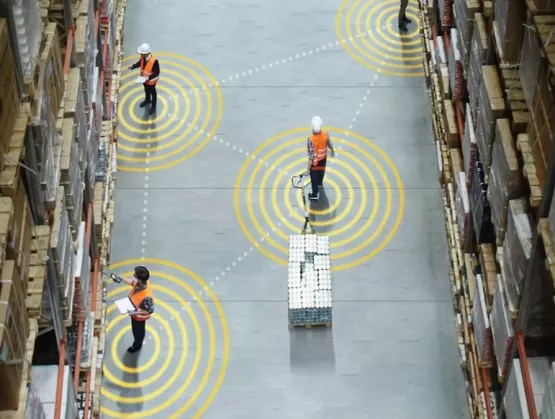
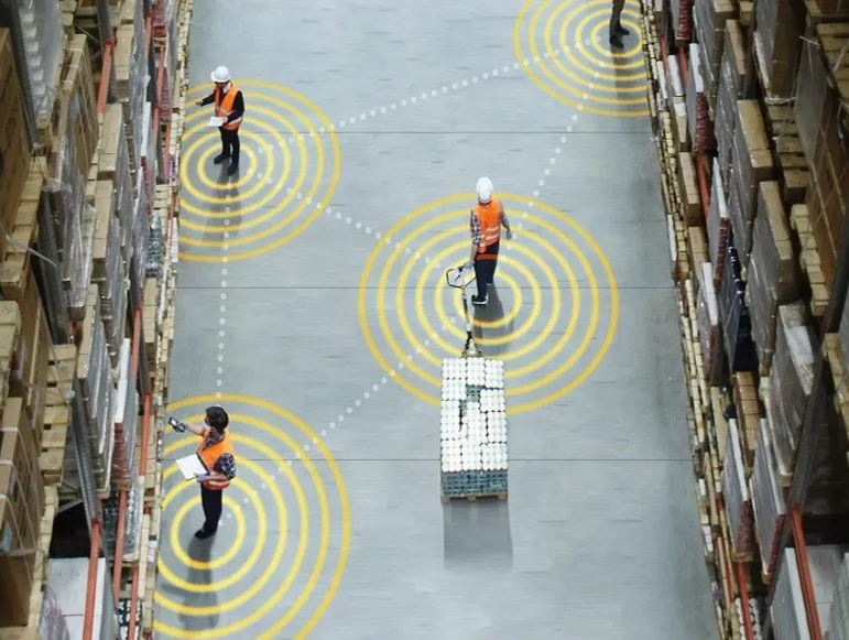
Earlier this year when the novel coronavirus, SARS-CoV-2, began sprinting around the world, public health officials told us that social distancing was the most effective way to slow its spread. We’re now many months into the pandemic, and social distancing, combined with mask-wearing, is still the best way to prevent new cases of the disease.On March 20, 2020, governors on opposite coasts, Gavin Newsom in California and Andrew Cuomo in New York, shut down their states, and other states soon followed. Only essential businesses, such as select retailers – grocery and hardware stores as well as pharmacies, for example – were allowed to remain open. Depending on location, however, it was days or weeks before strict social distancing measures were in place. Tape stuck six feet apart on store floors has helped shoppers keep their distance. But shouldn’t there be a more exact and reliable way to gauge social distances in retail stores, gyms, workplaces and other settings?David Horsley, founder and CTO of Chirp Microsystems, a TDK Group company, believes so, and the company is developing technology that does just that. Horsley will share the details in his keynote A Wearable Social Distancing Solution Based on Ultrasonic Time-of-Flight Sensors October 14 at MSEC 2020, SEMI’s first virtual MEMS Sensors Executive. The event is October 6-8 and 13-15, 2020. Register now for MSEC 2020.I spoke with Horsley to learn more about the sensors.SEMI: What was the inspiration for providing Chirp’s ultrasonic Time-of-Flight (ToF) sensors for social distancing?Horsley: Companies actually started contacting Chirp about six months ago to inquire about social distance tags to measure distance between people. They already knew about us because we’ve been supplying MEMS ultrasonic ToF sensors for virtual reality and robotics for several years, so they knew we could provide the same kind of low-power range-finding accuracy for resource-constrained devices. SEMI: How are your customers using Chirp-based social distance tags?Horsley: They’re designing Chirp’s ultrasonic ToF sensors into wearable tags worn by workers in distribution centers, in factories, and in oil and gas production, to name a few areas. The tags alert workers when they’re closer than two meters from another worker to ensure social distancing. Chirp’s ToF sensors also support contact tracing without recording any personal information, which is a major advantage over contact-tracing applications from companies like Google and Apple. Because those apps use Bluetooth Low Energy (BLE), which is already in your smartphone, the user has to enable location services. This records your GPS location, a privacy concern.BLE is problematic on some other levels as well. It only provides one-meter accuracy while Chirp’s ToF solution for social distancing delivers one-centimeter accuracy. Because BLE is only accurate within one meter, it can’t alert you in real-time that you’ve crossed that two-meter boundary to another person. Imagine you’re in the checkout line at the supermarket. BLE can tell you that other people are in your general vicinity, but it doesn’t have enough resolution to tell you whether the next shopper is two meters away from you or only one-and-a-half meters away. And because it doesn’t use the air as a medium, it registers a lot of false positives. If, for example, you’re separated from a person by a partition or a wall, and you’re within two or three meters of each other, your phone’s social-distance app will register a false positive.SEMI: Are you talking with customers in other environments, such as college campuses and theme parks?Horsley: There’s great deal of potential in those markets. For example, Professor Prabal Dutta’s group at UC Berkeley is working on a system that uses our sensors. His work also made us aware of some of the privacy concerns around contact tracing because universities are much more uneasy about student privacy than some private-sector companies are today. SEMI: What would you like MSEC attendees to take away from your presentation?Horsley: From the beginning, we believed that MEMS ultrasound was very versatile. We expected it to find a home in different types of applications because of its low power, small size and ease of use, particularly since we provide the enabling software that makes it all work. With design wins in four to five vertical markets, we’re experiencing significant marketplace validation. We’re all hoping that COVID-19 will wind down in the first half of 2021. As the focus on social distancing begins to fade, we’re looking forward to building out our customer base in the markets we’re in today as well as gearing up to explore new markets.Chirp Microsystems and TDK InvenSense are longtime members of MEMS Sensors Industry Group® (MSIG), a SEMI technology community that connects the MEMS and sensors supply network in established and emerging markets, enabling members to grow and prosper. Visit us today to learn how MSIG membership can make a difference in your business.David A. Horsley, Ph.D., is co-founder and CTO of Chirp Microsystems Inc., a TDK Group company. Horsley is also a professor of Mechanical and Aerospace Engineering at the University of California, Davis, and is adjunct professor of Mechanical Engineering at the University of California, Berkeley. Since 2004, he has been co-director of the Berkeley Sensor and Actuator Center (BSAC), the National Science Foundation’s Industrial/University Collaborative Research Center (I/UCRC) focused on MEMS research. Horsley is also a recipient of the National Science Foundation’s CAREER Award, and has authored or co-authored over 150 scientific papers and holds over 20 patents.Maria Vetrano is a public relations consultant for MSIG, a SEMI technology community.
Read More
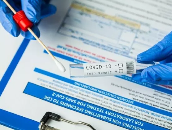
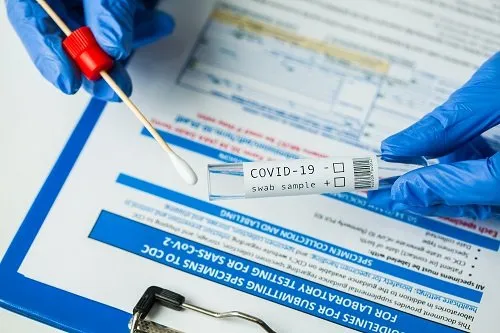
While the world awaits a working vaccine to protect us from COVID-19, we need to employ all available tools to help curb the spread of this novel virus. On the one hand, it’s remarkable that we’re relying on the same low-tech tools that our forebears used to moderate the pandemic of 1918 — social isolation, mask-wearing and hand-washing. On the other, we have access to numerous technologies that hadn’t even been invented a century ago. Among the most important is molecular diagnostics for advanced testing.While we continue to face a scarcity of test kits in the U.S., the majority of commercially available genetic tests for COVID-19 are reliable, so accuracy is rarely the problem. We’re hampered instead by the timeliness of getting the results and by the level of detail the tests provide.To save more lives and reduce the burden on our healthcare system, we need point-of-care genetic tests that deliver accurate results rapidly, telling us right away who’s positive and who’s negative. We also need pertinent test data shared as quickly as possible via secure networks to improve our ability to track surges in infections. These are two of the challenges that emerging biotech companies are pivoting to embrace. RT-PCR: The Gold Standard in Accuracy, Not SpeedWhen I read about some of the high-quality COVID-19 tests on the market – such as Abbott’s, which detects positive results in as little as five minutes — I am awed by how far we’ve come since the last global pandemic. The core enabling technology in test platforms such as Abbott’s uses the molecular genetics technique real-time reverse polymerase chain reaction (RT-PCR). The vast majority of rapid tests administered today in hospitals and other clinical settings use RT-PCR.While accuracy is high for RT-PCR tests, getting tests results to patients is slow because test samples are sent to the lab for analysis. That lab could be located in a hospital, in a doctor’s office, or in an urgent care facility run by a large company such as Quest Diagnostics. Regardless of location, each lab must have an RT-PCR machine to read the test results. Plus each RT-PCR machine costs thousands of dollars, and requires a technician to read the results, , factors that have limited the proliferation of these machines.New COVID-19 cases are still surging in parts of the U.S., India and Brazil, and in some areas, we’re seeing instances of inundated labs, with test results coming back in one to two weeks. That’s not fast enough for a virus this contagious. We need to get accurate tests results to healthcare providers, public officials, and patients as close to real-time as possible. To meet this goal, we need to apply molecular-diagnostic techniques to new types of biosensors that deliver test results at the point of care in minutes through platforms that send that data in near real-time to the cloud. This essential information will allow public health institutions, states, cities and other key stakeholders to identify and mitigate emerging hot spots of disease.Over the past seven months, we’ve had the privilege of working with a handful of biotech companies that have pivoted to develop rapid point-of-care molecular diagnostics that target COVID-19. One of these, HEMEMICS, is developing a handheld molecular diagnostic test platform that could be administered by healthcare workers in triage settings such as ambulances, emergency rooms, community clinics and makeshift hospitals. As a true point-of-care test platform, it would deliver results onsite, without requiring the transfer of test samples to a lab. “We’re aiming to redefine point-of-care testing for COVID-19,” said John Lehman Warden, Jr., CEO and co-founder, HEMEMICS. “Unlike the most common type of on-site test — the lateral flow monitor — our test isn’t waiting for osmotic reactions to occur. We place the sample from a quick nasal swab or a drop of blood right on-chip, and binding takes place within a standing drop of fluid. That makes our platform fast, delivering results in about 60 seconds. Plus it simplifies sharing test results with other communities of interest, such as public health departments and municipalities, because it’s Bluetooth-enabled and supports cloud-based management networks.”As its foundry partner, we’re collaborating with HEMEMICS as it continues to refine its biochip’s sensitivity for both antibody and antigen testing of SARS-CoV-2. Once HEMEMICS is satisfied, it will move forward with the U.S. Food and Drug Administration’s (FDA’s) emergency use authorization (EUA), which it hopes will bring the HEMEMICS platform into the hands of the millions of people who stand to benefit.As we head into the fall and winter months, we’ll need both rapid, connected point-of-care biosensor test platforms such as HEMEMICS’ and high-accuracy RT-PCR tests to fight COVID-19 effectively. And at their root, we’ll have MEMS and biosensors to thank. For more information on Rogue Valley Microdevices’ biosensor solutions, please contact the company at [email protected] or visit its website. As founder and CEO of Rogue Valley Microdevices, Jessica Gomez has created a world-class precision MEMS foundry in the heart of Southern Oregon. Integral to her role as CEO, Gomez practices a business philosophy of offering best-in-class process technology and R D expertise to customers to help them achieve the highest quality and reliability in their products. Gomez plays an active leadership role within and beyond the technology industry. She is a board member of the prestigious SEMI Board of Industry Leaders, she was the first executive selected for Spotlight on SEMI Women, and she is chairman of the Oregon Institute of Technology Board of Trustees.Rogue Valley Microdevices is a longtime member of MEMS Sensors Industry Group (MSIG), a SEMI technology community that enables the MEMS and sensor industry to address common challenges, innovate and accelerate business results.
Read More
About 70% of the U.S. Gross Domestic Product (GDP) is driven by consumer demand. What consumers are looking for is influenced by, for example, fashion trends, product innovations, environmental forces, and personal interests. Regarding personal interests: Sales of electronic components at Fry’s are poor. Radio Shack stores even vanished completely. Today’s consumers do not like to tinker; they want to buy software-enabled, user-friendly systems with over-the-air updating that serves their current and future requirements well – e.g. smartphones. System vendors followed the same transition, and so did semiconductor vendors. Instead of offering (low margin) components, they develop and manufacture big portions of, if not complete, (high value) hardware and software solutions for electronic systems, targeted at specific markets.Mid-August, two SEMI webinars outlined the Smart Mobility market and what it expects from system and semiconductor vendors.SEMI's Smart Initiative“None of us knows as much as all of us,” “Connect – Collaborate – Innovate,” and other strategic considerations have motivated SEMI to become the gateway for the $2 Trillion (= 2,000 Billion) global electronic design and manufacturing supply chain. Figure 1 shows how many companies and organizations have joined this large industry organization, to work together efficiently and serve customer demands cost-effectively. Especially in four high-growth markets/application areas – Smart Data, Smart Mobility, Smart MedTech, and Smart Manufacturing – SEMI enables highly rewarding cooperation. Figure 1: Overview of SEMI members, technology communities, and areas of focus. (Courtesy: SEMI) MEMS and Sensors for Smart Mobility Tim Brosnihan, executive director of MEMS Sensor Industry Group (MSIG), moderated the webinar on MEMS and sensors for Smart Mobility. Bettina Weiss, Chief of Staff and Global Smart Mobility Lead at SEMI, presented the overview. In addition to Figure 1 above, she showed how many companies are now supporting SEMI’s Smart Mobility efforts and have joined the Global Automotive Advisory Council (GAAC). The European GAAC was founded in 2018, based on requests from VW and Audi. Regional chapters have also been formed in the U.S., China, Taiwan, and Japan. Figure 2 shows the current members of the American GAAC – new members are welcomed in all five regions. Figure 2: Current GAAC members in the Americas. (Courtesy: SEMI) Market Trends and Technology Innovations in MEMS Sensors Andreas Breiter, Partner at McKinsey Company, addressed markets, and Armen Mkrtchyan, Associate Partner at McKinsey Company, spoke about technology. Breiter addressed both vehicle and infrastructure changes required, as well as many ongoing and planned activities to enable Smart Mobility. He outlined autonomy, connectivity, electrification, and shared mobility of vehicles as the major opportunities for MEMS sensors. Mkrtchyan showed which technologies enable Smart Mobility and which regions will invest how much in software, hardware, and services by 2030, to capture data and process it in partially/fully autonomous vehicles’ Domain Control Units (DCUs) – see Figure 3. Figure 3: Pre-COVID market estimates. (Courtesy: McKinsey Company) MEMS-based sensors are used in vehicles to monitor pressures and perform as accelerometers or gyroscopes. Non-MEMS-based sensors capture light (e.g. for time-of-flight distance measurements) or magnetic fields (e.g. for RPM measurements). Regarding the many infrastructure upgrades needed for enabling autonomous vehicles on the roads, in Figure 4, Breiter gives road planners a lot of food for thought and planning work. City planners face much more complex challenges. That’s why electronic systems will also be needed to make these large infrastructure investments earn returns. Figure 4: Smart roads are essential for autonomous driving. (Courtesy: McKinsey Company) EDA and Smart Mobility The second Smart Mobility webinar focused on how Electronic Design Automation (EDA) tool vendors, Intellectual Property (IP, System Building Blocks) vendors, and system/IC Design Services can contribute to the success of Smart Mobility. Bob Smith, executive director of Electronic System Design Alliance (ESDA), moderated the webinar, highlighting where the relatively small but essential ESDA and its members fit in the semiconductor ecosystem – see Figure 5. Figure 5: EDA, IP, and design services enable the entire electronics ecosystem. (Courtesy: ESDA) Bettina Weiss explained how SEMI and the Smart Mobility Team are working to bring together stakeholders in the semiconductor ecosystem in general and the Smart Mobility segment specifically, to jointly address topics of common interest, work on solutions and agree upon standards where and when needed. Market Trends and Technology Innovations in EDA, IP and Design Services Andreas Breiter and Armen Mkrtchyan presented McKinsey’s perspectives regarding these topics. In addition to the above-mentioned market data, Breiter emphasized that DCUs are playing an increasingly important role in capturing the data provided by smart sensors, are processing it, and initiating appropriate actions. Together with application-specific software, these DCUs perform tasks like sensor fusion, manage creature comfort, assure safe operation of the vehicle, and secure communication with the outside world (Figure 6). Figure 6: High growth for DCU; likely shift in business models. (Courtesy: McKinsey Company) Mkrtchyan addressed EDA, IP, and services for Smart Mobility from 10 different technical perspectives. Here are the highlights. Component failures can and will have severe consequences in Smart Mobility. Therefore screening, testing, and exhaustive verification are extremely important. Software content is likely to increase at 10% CAGR during this decade. To increase the productivity of software and middleware developers, he emphasized that standards need to be agreed upon. Over-the-air (OTA) updating capabilities are needed. That’s why cybersecurity is important to keep vehicles current and safe. Power train electronics need to function at up to 150°C. New materials will be needed to increase reliability, reduce cooling efforts, and lower unit costs. Last, but not least, Mkrtchyan emphasized that every city needs to design its own infrastructure, not only to enable Smart Mobility but also to monetize the large investments needed; EDA, IP and design support will help to achieve both. In summary, he stated that Design and IP as well as packaging and test will be the most impacted areas in the transition to Smart Mobility. Personal Comments After having attended several MSIG events, I am impressed by how MEMS, NEMS (Nano…), and sensors can lend machines in many ways sight, smell, taste, touch, and hearing. They can replicate these human senses, often better than found in us. If you, like me, celebrated when your first modem enabled your PC to communicate with the entire world, you’ll appreciate the value MEMS and sensors can and will add to machines’ “communication skills.” Also, I can assure you that innovative engineers in this field will find many new ways to capture data in the physical, chemical, and biological domains and enable machines to keep humans safe. (I look forward to a handheld Covid-19 sensor that provides results within a few seconds!) Having worked for a small, then a large EDA vendor, many years ago, and for the ESD Alliance several years ago, I know how difficult it is to motivate innovative software developers to work together or agree upon standards. I am glad that the ESD Alliance is now working closely with SEMI. Most SEMI member companies, and their innovative employees, have learned over the years how important standards are to reduce development cost, processing, and test time, as well as time to profit. I wish Bob Smith and the ESDA members all the best for cooperating closely to define design standards, bi-directional hand-off points up and down the entire supply chain, primarily at the interface between design and manufacturing. I want to encourage EDA and IP experts to work closely with the experienced and knowledgeable people in materials, equipment, manufacturing, and test. 5G mm-wave communication, artificial intelligence/machine learning (AI/ML), reliable solutions for Smart Mobility, and development/characterization of new materials offer great opportunities and challenges for design AND manufacturing. Together, these two big camps can monetize required solutions much better and faster, than on their own. Your contact at SEMI can tell you how and where you can watch the webinar recordings and/or download all the slides. P.S.: Having two eCars and one eBike in our garage encourages me to appreciate SEMI’s efforts in advance Smart Mobility! Republished with permission from 3D InCites.
Read More
Inertial sensors have continued to underpin the success of wearables in increasingly important ways. Propelled by evolutionary advancements in inertial sensors, wearables have strayed from their humble beginnings in simple activity and wellness, which defined the user experience over the past decade. What started with the simple act of telling people their daily step count has morphed to provide deeper insights into swim stroke and run cadence, all the way to mapping out a person’s off-piste ski route. Layered on top of this foundation of inertial sensors, we’ve fused optical, temperature and other sensor technology to provide clinical-grade healthcare snapshots available previously only by visiting the doctor’s office.Inertial sensors today are again leading the way in improving health and wellness. Instead of humans, however, this time the patients are machines. In fact, the health of critical assets – whether factory-based equipment, windmills, train bogies or aircraft – has been assessed through sophisticated analysis of their vibration signatures for many years. The sensors used for these applications have depended on piezoelectric technology because their vibration amplitude signals are very small and difficult to detect and because of the importance of understanding their spectral content over a wide bandwidth. When it comes to noise and bandwidth, bulk piezoceramics have had a major advantage over electrostatic MEMS technology – until recently.Using bulky expensive piezoelectric sensors for condition-based monitoring has been akin to going to the doctor’s office to have an MRI. The equipment required (sensors, receivers) is expensive and requires highly trained specialists to operate the machine and to interpret the information. For this reason, only mission-critical assets are instrumented. For nearly all other equipment, we tend to use inefficient schedule-based maintenance approaches to cover the gap of not having continuous data. Condition-based monitoring leverages real-time sensing of critical machine parameters to reduce system downtime and improve efficiency. Evolving machine healthMEMS started to democratize machine health several years ago, when suppliers began switching from piezoelectrics to capacitive MEMS. While the performance was still not on par with piezoelectric sensors, MEMS technology could already capture a wide array of faults. One example, the ADXL001, started making its way into Integrated Electronics Piezo-Electric (IEPE) and 4-20 mA sensors, which form the backbone of the vibration monitoring market. Although the bandwidth and noise of the sensor did not allow for very early detection and prescriptive monitoring, it did allow the tracking of faults as they progressed and became more imminent.Other digital accelerometers started finding their way into new wireless prototype systems with the goal to simplify and increase deployment to a greater population of assets. The thinking was that self-contained digital wireless sensor nodes could be deployed more economically and quickly, and that these digital sensors would bring the power of computing to the edge node.Unfortunately, even the lowest-noise MEMS products did not have the bandwidth needed to diagnose and predict faults early enough to influence how and when machines are maintained most economically. Instead, such devices were used to detect imminent failure to prevent irreparable harm. As we all know, however, the earlier the doctor spots a problem, the better the probable outcome. That’s because early detection increases the likelihood that the doctor will have access to the full spectrum of treatment options available to fix the problem.Inertial MEMS is blazing a new frontier with the introduction of next-generation capacitive MEMS such as the ADXL100x portfolio. Offering ultra-low noise density and high-frequency response, these newer capacitive MEMS devices fit the bill. With 3dB bandwidths up to 25 kHz and flat response curves within 0.4dB all the way to 10kHz, these accelerometers demonstrate compelling enabling characteristics such as better DC performance, improved robustness, lifetime stability, linearity, and of course, cost, making capacitive MEMS a better choice than piezoelectrics.With high-bandwidth capacitive MEMS much easier to use and deploy – as well as more affordable – the market is starting to respond. Condition monitoring equipment and instrumentation is becoming more accessible to a larger base of manufacturers. In turn, a wealth of data is being created and mined to develop better and timelier predictive and prescriptive maintenance approaches that rely heavily on machine learning and artificial intelligence (AI).It’s worth paying attention to the sizable condition-based monitoring market. Estimated at $3.5 billion and growing, condition-based monitoring reduces downtime and increases equipment utilization in quantifiable ways. And it’s not just manufacturers who stand to benefit. More sustainable and efficient industrial processes, safer trains that crisscross continents at ever increasing speeds, autonomous cars and trucks that know what’s happening under the hood as well as on the road, and modern infrastructure to support our evolving lives show us that condition-based monitoring has something for everyone.Learn more about Analog Devices’ condition-based monitoring signal-chain options that help customers on the journey from sensor to solution. View ADI’s whole portfolio of condition-based monitoring solutions online or download Next-Generation Condition-Based Monitoring brochure.Tzeno Galchev is product marketing manager in the Inertial Sensor Technology Group at Analog Devices Inc. He oversees the strategic marketing and product definition of the inertial sensor component portfolio. He received B.S. degrees in both Electrical and Computer Engineering in 2004, and M.S. and Ph.D. degrees in Electrical Engineering in 2006 and 2010 respectively from the University of Michigan, Ann Arbor. He has over 30 publications in the area of MEMS, holds multiple patents, and is a frequent lecturer and speaker on topics related to MEMS, energy harvesting and sensors.Analog Devices is a longtime member of MEMS Sensors Industry Group (MSIG), a SEMI technology community that enables the MEMS and sensor industry to address common challenges, innovate and accelerate business results.
Read More
Why do we need environmental air pollution sensors?Today we need environmental air pollution sensors more than ever to ensure that we have clean and safe outdoor and indoor air. Although federal rules have improved air pollution over the past several decades, more than 110 million Americans still live in counties where air quality is below national standards. An estimated 100,000 Americans die prematurely each year of illnesses caused or exacerbated by polluted air.“Cars and trucks are much cleaner than they were, power plants are cleaner, industrial operations are cleaner,” said Paul Billings, Senior Vice President Advocacy for the American Lung Association. But cleaner air is not clean air.”While scientists have long known that air pollution may exacerbate asthma and other respiratory illnesses, new data suggests polluted air leads to higher COVID-19 higher death rates and brain inflammation that can contribute to dementia and autism.To understand the importance of air quality and how we can apply existing sensors and develop new ones, we look both outdoors and indoors (see Figure 1). Outdoor air quality relates to gaseous and particulate pollutants, defined by the Air Quality Index (AQI). The AQI became a standard based on regional thresholds for a set of key outdoor pollutants: four gaseous pollutants (sulfur dioxide, nitrogen dioxide, carbon monoxide, ozone) and particulates (PMs) of different sizes such as 10 μm (PM10) and 2.5 μm (PM2.5). At present, the AQI is measured using traditional analytical instruments. Despite their high acquisition and maintenance costs, these instruments are the only solution to accurately measure these pollutants in the presence of variable environmental background.Figure 1. Examples of outdoor and indoor air quality markers Indoor air quality (IAQ) is also of growing concern. Formaldehyde, benzene, carbon monoxide, and carbon dioxide are some of the key pollutants with restricted concentration levels in residential, office and industrial buildings. Sources of these and other gaseous pollutants include building materials and equipment, workplace cleansers, and building occupants. Regulatory agencies and building occupants use different methodologies to estimate IAQ using gaseous and particulate pollutant analyzers. These estimates also consider air humidity and temperature that affect indoor air quality. Where are we today with environmental sensors?The top three requirements for modern gas sensors include: the sensor reliability to provide accurate readings in diverse environmental conditions over desired period of use low power, to extend battery life or to eliminate its need, and low cost, to facilitate their ubiquitous deployments. Advances in electronics, microfabrication, and packaging have delivered recent important developments in reducing the power consumption and miniature packaged solutions. Recent R D efforts are also increasing the number of successful gas sensor field deployments for outdoor and indoor air quality monitoring. Figure 2 illustrates three examples of recent developments in gas sensors that meet requirements of diverse customers.Electrochemical sensors from SPEC Sensors were collocated with EPA instruments for monitoring of NO2 and O3 in Chicago’s Array of Things Project. Figure 2A shows that these new cost-effective sensors track well the EPA instruments. Advancements in circuit quality, sampling, enclosure design, and initial calibration/compensation were all essential in achieving these results. While this example clearly demonstrates the usability of these sensors in this particular application, the expectations that low-cost, off-the-shelf sensors will match the performance of EPA reference systems that cost 50x-100x more must be adjusted. A micropackaged sensor suite from Bosch Sensortec includes sensors for total volatile organic compounds (TVOCs), temperature, humidity, and pressure. TVOC measurements are needed according to the guidelines by the German Federal Environmental Agency. To report TVOC, the sensor algorithm tracks the TVOC-related resistance of the metal oxide sensor, corrects sensor resistance for ambient temperature and humidity, and outputs the TVOCs Index of Air Quality between 0 (clean air) and 500 (heavily polluted air) as shown in Figure 2B. A recent GE-developed dielectric excitation scheme of metal oxide sensing materials provided a highly desired and long-awaited calibration stability of sensors for monitoring of fugitive methane gas emissions in all-weather conditions. These sensors were used in several field validation campaigns in Oklahoma, North Dakota, Arkansas, and British Columbia and had stable performance after more than 400 days, as compared to an initial calibration (see Figure 2C). Such stable sensor performance has become possible by switching from the conventional resistive mode of operation of metal oxide sensing elements to the dielectric excitation scheme. Figure 2. Examples of applications of contemporary gas sensors based on different detection principles.(A) Outdoor performance of NO2 and O3 electrochemical sensors versus EPA-validated instruments.(B) Calibration results of a BME680 metal oxide gas chemiresistor upon exposures to TVOCs (blue stair-profile) and its ± 15% confidence interval band as the Index of Air Quality.(C) Calibration stability of a sensor with an innovative dielectric excitation scheme implemented for monitoring of fugitive methane gas emissions after multiple uses in diverse field validation campaigns. Key challenges and solutions toward realizing new applicationsIn this era of data-on-demand, environmental sensors could enable countless new applications. Imagine you have a gas sensor conveniently integrated into a smartphone or a watch. You are commuting to work, and your sensor alerts you that the subway station through which you are traveling has very poor air quality. How might this alert affect your behavior? Would you put on a mask, change your commuting route to a twice-longer one, or petition the city? What if you are attending a parade downtown with your asthmatic child, and your device informs you that the air is clean? Would you skip the parade if you knew that your sensor was only 10% accurate? How would you avoid a risk of ending with your asthmatic child in a hospital?Design principles of modern sensors originate in the 20th century for detection of high gas levels from leaks, but they did not anticipate the applications proposed now. By design, existing sensors have only a single output – e.g. resistance, voltage, current, light intensity – that mathematically cannot correct for the sensor instabilities caused by the complex chemical background and variable temperature and humidity conditions. Thus, often these simple sensors perform best when pollution levels are high and when the compound of interest swamps others. As a practical example, there are dozens of gaseous pollutants in ambient air with their toxicity that differ 1,000-10,000 fold. Often, the insufficient reliability and accuracy of existing sensors in the field conditions is a significant bottleneck toward the broad adoption of gas sensors. According to the United States Environmental Protection Agency (EPA), the correlation between readings of low-cost sensors versus reference monitors varies widely from 1% to 80%. The EPA also states that no low-cost sensors meet Regulatory Monitoring requirements, and the World Meteorological Organization emphasizes that “low-cost sensors are not currently a direct substitute for reference instruments, especially for mandatory purposes.” However, we now have the increasing number of examples of reliable operation in complex environments (Figure 2) in addition to important advances in reduced power and size of contemporary sensors. Still, the key challenges to realize new applications are often the lack of required accuracy and reliability of available sensors for new contemplated applications.Is it possible to offer low-cost sensors for at least some applications and some gases with the degree of accuracy approaching more expensive specialized instruments? We, the SEMI-MSIG Device Working Group, are saying: Yes. To deliver on this bold statement, our SEMI community brings new technological solutions to the 100-year old general design of gas sensors.Our next blog What is in the Air will provide details on our activities of SEMI-MSIG Device Working Group to establish standards and new measurement schemes to reduce effects from uncontrolled ambient conditions and to improve stability, limit of detection, and dynamic range of environmental sensors. Also learn how new MSIG members can impact this important working group. The MEMS Sensors Industry Group (MSIG) is a SEMI technology community that enables the MEMS and sensor industry to address common challenges, innovate and accelerate business results.Radislav A. Potyrailo is Principal Scientist, Micro Optoelectronics Gas-Chem-Bio Sensors Systems, at GE Research; Ed Stetter is General Manager at SPEC Sensors, LLC; Ryotaro Sakauchi, is Senior Manager of Business Development at Bosch Sensortec; Merry Smith is a Product Manager and Senior Scientist at C2Sense, Inc.; and Sreeni D. Rao is Senior Director of the MEMS Business Group at TDK Corporation.
Read More
A lot has happened in fifty years, particularly when it comes to the microelectronics industry. Founded in 1970 by a group of semiconductor industry pioneers who believed that co-opetition — instead of traditional competition—would produce a more vibrant emerging industry, SEMI was born as an industry association.It's fitting during this week’s 50th annual SEMICON West (July 20-23, 2020) — a virtual event for the first time — that SEMI Chief of Staff Bettina Weiss offers her perspectives on the evolution of SEMI from one of the best seats in the house: the 24 years that she has spent helping the association change and grow.Vetrano: You’ve enjoyed a long rich history with SEMI, and now serve as the association’s first chief of staff. What roles have you played at SEMI up to this point?Weiss: I cut my teeth at SEMI by joining SEMI Standards, first serving as standards coordinator at SEMI Europe from ’96-’97. Over the next 11 years, I held a variety of positions at SEMI Standards, culminating with director of international standards from 2003-2008. Given that experience, I have to admit that SEMI Standards are still near and dear to my heart.I moved on to several leadership positions in our former global photovoltaics/solar business through 2014, and toward the end of that stint, I assumed additional responsibilities, becoming vice president of business development. That’s where I dove headfirst into expanding SEMI into emerging regions, including Vietnam, India and Latin America. SEMI goes where members see (or want to better understand) new opportunities, especially in places that had ambitious plans for fabs for microelectronics, including semiconductors and MEMS.In 2018, I became SEMI chief of staff, reporting directly to our president and CEO Ajit Manocha.Vetrano: Now I hardly know where to start! Since I have to decide, what does it mean to be SEMI chief of staff?Weiss: As the first chief of staff, I’ve been able to shape the position, combining the support of critical efforts driven by Ajit with additional project management responsibilities like our Smart Mobility initiative.Working with experienced leaders in our industry, such as the Board of Industry Leaders (BIL), is one of the more rewarding parts of my role at SEMI. The BIL is a group of global executives tasked with advising SEMI on strategic planning, especially when it comes to future-looking initiatives like Smart Mobility, Smart MedTech, Smart Manufacturing, and Smart Data/AI.A lot of the other things I do are meant to support the whole SEMI organization, in partnership with other senior leaders such as Michael Ciesinski, vice president of technology communities, as we create business plans and examine new revenue models that will keep SEMI sustainable and viable for the future. This includes issues as varied as workforce development and diversity and inclusion, and the new digital platforms we use to engage with our members.Vetrano: How does SEMI Smart Mobility initiative exemplify the model of engaging end customers in vertical markets that are important to members?Weiss: When you look at the rapidly increasing number of chips and sensors in and around vehicles, Smart Mobility at its core brings together both the semiconductor/sensor and automotive/mobility supply chains for a more transparent dialogue about needs and wants along the entire supply chain. We are thrilled to count automotive OEMs Volkswagen and Audi as SEMI members. We also work with Tier 1 suppliers such as Continental and many others to promote the open exchange of ideas and foster collaboration among all stakeholders.Smart Mobility is a good example of how SEMI connects two worlds that are now interdependent for the mutual benefit of all players. Automotive companies and component suppliers want to better understand new technology capabilities that enable tomorrow’s infotainment, safety, security and communication protocols. And semiconductor, sensor and component companies see huge upside in supplying the equipment, materials, devices and subsystems that enable the future of mobility. Smart Mobility is a win-win, and the founding concept of our Global Automotive Advisory Council (GAAC).Vetrano: As we look to COVID-19, the single most important event to influence the microelectronics industry — and every other industry — why is SEMI membership more important now than ever?Weiss: Our industry is facing a triple whammy of challenges: a global pandemic, ongoing global trade tensions that impact interdependent supply chains, and a global economic crisis. All these challenges will require our members’ ingenuity, innovation and collective action to overcome them. But inherent in those challenges are tremendous opportunities, and I have no doubt that our members and the entire global electronics ecosystems will find ways to help everyone prosper and advance.COVID-19 has had a huge impact on our members. From the onset of the pandemic, we’ve provided our members with resources including best business practices, insights and data from industry experts to help them respond to a virus that has already changed so many things we took for granted before March. Additionally, SEMI has also advocated with governments around the world on behalf of the industry for essential business status and essential travel to sustain operations. Visit SEMI COVID-19 Resource page for information on industry best practices and much more.Vetrano: Before we look forward, what has changed dramatically in microelectronics since you started at SEMI?Weiss: Through my work with SEMI, I’ve witnessed dynamic, dramatic and sustained change in the microelectronics supply chain. Into the late 1990s, SEMI represented primarily semiconductor equipment and materials suppliers, and we worked with chipmakers – our members’ customers. That’s where a lot of important Standards work happened, for example, and the supplier-device maker relationship was pretty much our world. Over the years, we saw significant change in how companies partner and do business with one another. The digital transformation we’ve been witnessing for the past few years was the impetus for expanding our reach to bring companies in the extended electronics manufacturing and design supply chain together, from sand to system, so to speak. That was also when we invited associations representing flexible hybrid and printed electronics (FlexTech), MEMS and sensors (MSIG), and electronic system design (ESD Alliance) companies to join SEMI and our other technology communities for maximum cross-pollination. That’s because everything needs microelectronic devices and systems. Vetrano: Looking ahead now, what is can the microelectronics industry do to benefit humanity?Weiss: Semiconductors and sensors are often the unsung heroes of progress. Microelectronics can help bring prosperity to the billions of people now struggling on our planet. It can improve access to education for people through e-learning, it can advance agricultural production and streamline the food supply chain to help feed the world’s hungry, it can monitor the quality of the water we drink and the air we breathe, and it can get you in front of a doctor even in the most remote village in India.The beauty of microelectronics is that we are not gated by innovation. As the brilliant visionary Arthur C. Clarke once said, “The only way of discovering the limits of the possible is to venture a little way past them into the impossible.”As an industry association that helps technologists to venture beyond “the limits of the possible,” I invite like-minded technology adventurers to engage with SEMI, starting with registration to this week’s SEMICON West – our first virtual show.As chief of staff, Bettina Weiss reports to SEMI President and CEO Ajit Manocha and manages a broad portfolio of responsibilities. Major focus areas include advancing specific global strategic initiatives such as thought leadership (Think Tanks) and SEMI Smart Transportation vertical application platform, improving organizational efficiency, alignment and financial sustainability, acting as senior liaison to SEMI Board of Industry Leaders, leading strategic partnerships and M A activity, and supporting Manocha in creating a highly effective, agile global association.Maria Vetrano is a PR consultant at SEMI.
Read More
Humanity has survived almost unimaginable challenges over the past 5,000 years of documented human history. From war, famine and natural disasters to the first global pandemic in the last 100 years, more often than not, people have relied on one another to survive and thrive again. As the industry association representing the global microelectronics industry, SEMI has similarly made collaboration and community integral to the fabric of its organization. From helping members to succeed through the COVID-19 pandemic to facilitating member-driven industry standards around environmental health and safety, materials, and manufacturing capabilities, this approach shows members that standing together is better than standing alone.On the eve of the 50th annual SEMICON West (July 20-23, 2020) — the first virtual edition in SEMI’s history — I spoke with SEMI’s vice president of technology communities, Michael Ciesinski, about the role of SEMI in tackling big challenges through an active member community intent on solving problems through collaboration.SEMI: How long have you worked with SEMI and in what capacity?Ciesinski: In January 2016, I started my second tour at SEMI when FlexTech, the industry consortium I’d been leading, became SEMI’s first strategic partner. Nearly two years into that role, SEMI President CEO Ajit Manocha asked me to form Technology Communities to engage members with common interests. After FlexTech, we brought on the Fab Owners Alliance, then MEMS Sensors Industry Group (MSIG), and later the Electronic System Design Alliance (ESD Alliance).SEMI now has more than 20 communities in all, including Smart MedTech, Smart Data AI, Smart Manufacturing, Electronic Materials, and Integrated Packaging, Assembly and Test.SEMI: What is your role with Technology Communities — and how do members stand to benefit?Ciesinski: The leadership of Technology Communities ensures that SEMI’s benefits and services align to our members’ interests so we can provide member benefits that matter most. This spans forming communities where people hold common interests (e.g., advanced packaging) to facilitating standards that will promote intelligence in manufacturing (e.g., data standards for AI and machine learning) as well as providing R D funding.I’m especially proud that over the past three years, SEMI has brought more than $40 million in R D funding to our members, with most grants in the $500,000-$1 million range. We’ve been especially successful in securing funding in flexible hybrid electronics (FHE) through U.S. Army Research Laboratories (ARL), a model we first developed through FlexTech.Two recent recipients of FHE funding, GE Research and ITN Energy Systems, show how the grants are spawning partnership opportunities among commercial enterprises, R D organizations and universities. In developing lightweight, non-invasive wearables, including a human-performance sweat-monitoring patch that remotely analyzes sweat to detect hydration levels and other vital signs, GE Research is using key components such as sensors and lightweight batteries in its designs.ITN Energy Systems designed a flexible all-solid-state lithium battery that’s printed on light, flexible substrates to power small and incredibly thin applications.Universities are also benefiting by plugging into the SEMI ecosystem. In fact, 40-50 percent of funded projects are seeding commercialization by universities. This is another validation that SEMI’s collaborative, community approach to microelectronics is working.SEMI: Position, Timing and Navigation (PNT) is another hot area where SEMI has secured ARL funding. What makes this funding different and why is it important?Ciesinski: The PNT grant makes ARL funding available to the MEMS Sensors Industry Group (MSIG) members through SEMI for the first time. If you’ve ever lost GPS signal while coming out of a tunnel, you know how frustrating that is. For us, that’s an inconvenience, but for a healthcare worker in a remote location who’s waiting for a delivery of medication by drone, it could be life-critical. While that’s just one example of why we need PNT to operate when GPS isn’t available, I can imagine dozens of other important dual-use cases, including autonomous driving.SEMI: How else do Technology Communities benefit under SEMI?Ciesinski: Technology Communities need access to diverse resources to spur continuous innovation. Electronic Materials Group participants, for example, need to stay informed on regulations coming out of Asia, the U.S. and Europe that may affect their businesses. Where else other than SEMI can like-minded stakeholders congregate with people up and down the supply chain to determine whether industry-wide action is needed on regulation?SEMI: What is the importance of SEMI’s global footprint?Ciesinski: I’ve worked with many associations and managed major industry consortia. The clear advantage of SEMI is our global footprint. And that’s vital because microelectronics is a global industry involving a multitude of stakeholders that play essential roles in the supply chain.Let’s say you want to discuss EU regulations on hazardous chemicals. Rather than decipher these complexities alone, you can pick up the phone to speak with someone on SEMI’s European team to learn what’s critical.What if you’d like more information on the 20-plus new fabs that are going up in China? You can explore that question with our SEMI China or SEMI Industry Research and Statistics teams.SEMI: How has SEMI evolved over the years?Ciesinski: SEMI has a long history of providing what the industry cares about. We started in trade shows and pivoted to industry standards. We began with small silicon wafers and wafer carriers, and now within the span of 50 years we’re working on data-format standards that will support the application of AI and machine learning (ML) in the semiconductor industry.While highly varied today, data-format standards will help component manufacturers refine processes to create more efficient solutions. This ARL-funded program, which pairs SEMI members with the grant recipient, Cornell University, may offer dramatic gains in the productivity of semiconductor manufacturing.SEMI: How does SEMI’s approach to COVID-19 reflect core values of collaboration and community?Ciesinski: Together with Ajit Manocha, CMO Terry Tsao and other team members at SEMI, we pulled together a task force to help SEMI members navigate the pandemic.We tapped two existing groups, Environment, Health and Safety (EHS) and Information Technology Leadership (ITL) from the start, documenting their strategic and tactical approaches to help all members through the COVID-19 resource section of our website. The EHS section provides tips on facilities and meetings, employee policies, business travel and communications, while the ITL section lists insights on computing hardware for staff, licensing, networks, security and employee policies.Our EHS leadership team, which includes Entegris, Axcelis, Versum, and Intel, immediately started sharing best practices for sanitizing facilities. As a result of team meetings, SEMI EHS shared best practices on keeping the workforce remote and guidelines for returning people to work safely. From securing PPE and safeguarding employees and visitors by performing thermal scanning to outlining communications around potential employee exposures, EHS has provided meaningful resources for the benefit of all members.SEMI also took immediate steps in the area of advocacy. Our advocacy team in Washington, D.C., together with regional SEMI presidents around the world, have ensured that semiconductor facilities were and still are considered essential businesses in the U.S., Europe and Asia. That’s because microelectronics are foundational to fighting the pandemic.Microfluidics are critical to the Reverse Transcription (RT) Polymerase Chain Reaction (PCR) tests most commonly used for COVID-19. Sensors are embedded in the pulse oximeters that allow patients and healthcare professionals to monitor a vital rubric: oxygen saturation level. If oxygen saturation level drops into the low 90 percentiles or below, it may be time to go to the hospital for treatment.Microcontroller units are essential components in a wide range of hospital equipment, including the ventilators that may make the difference between life and death in the most seriously ill patients.SEMI: How can the ingenuity realized through microelectronics continue to help us tackle other big problems? Ciesinski: We have MEMS and sensors to thank for distributed intelligence, giving us the ability to put sensors anywhere, locally based in the field or in the packaging house.Food production is a prime example. Leveraging miniaturized wirelessly connected sensors, we can trace food through the entire production lifecycle, from the seed in the ground to the food in the warehouse and, ultimately, to the product that lands on the table.From larger enterprise such as IBM Food Trust to small startups, we’re using MEMS and sensors to improve crop yields so we can feed a human population that’s growing each year.There’s a sustainability piece as well. We’re using MEMS and sensors to reduce the amount of fertilizer or other nutrients or chemicals in the soil. That’s good for the environment and for the agricultural workers who labor in the fields.MEMS and sensors can also condense the time it takes to perform a specific task, conserving human resources.SEMI: Where do you think SEMI will go in the next decade?Ciesinski: Ten years from now, I believe we will still have our global footprint in place. I expect it will expand, particularly in Asia.We may also expand into new areas such as Latin America and Central America, which would provide at least two major benefits: People working in microelectronics would, I hope, have access to better quality of life. And diversifying the supply chain would allow nations and regions to have more control over the products they need, from PPE to medications, which may help us to better manage through the next pandemic.I am also hopeful that SEMI will be on the leading edge of helping our members communicate in much different fashion from what we have today. We’re already expanding beyond the paradigm of in-person meetings for standards meetings and conferences. As we move forward, I think we’ll see a hybrid solution to doing business, combining in-person meetings with virtual conferences and digital content that’s available 24/7.Whatever changes we see in SEMI, I’m confident that we will continue to see a global footprint in an industry association that prioritizes connections among members.Engage in the SEMI experience at upcoming SEMICON WestRegister today to hear from keynote speakers such as environmental advocate and former U.S. Vice President Al Gore, futurist and author Steve Brown, and IBM Research senior vice president and director Dr. John E. Kelly III, and Lea Gabrielle, special envoy of the Global Engagement Center for the U.S. State Department, at SEMICON West , July 20-23, 2020. Content will be live streamed and available on-demand. Michael Ciesinski is vice president of Technology Communities for SEMI, the global microelectronics industry association, appointed in August 2018. At SEMI, he directs activity for more than 20 industry groups, oversees the association’s R D funding program, and develops new technology initiatives to serve SEMI’s 2,400 members. Prior to re-joining SEMI, Ciesinski was president/CEO of FlexTech Alliance, an industry consortium focused on new methods of creating electronics. From 1995-2008, Ciesinski served in a similar role at the U.S. Display Consortium (USDC), a private/public partnership chartered with building the infrastructure for electronic display and flexible electronics manufacturing. Both FlexTech and USDC annually sponsor multimillion dollar technology development programs and provide industry technical, financial and market services. Ciesinski is a graduate of the University of Albany, NY, and a former member of the Dean’s Advisory Committee at California Polytechnic State University.Maria Vetrano is a PR consultant at SEMI.
Read More
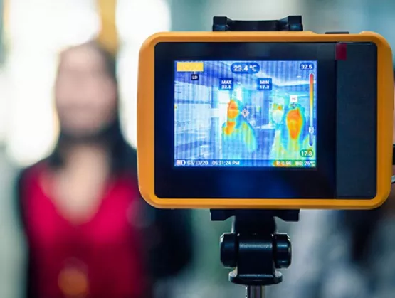
(The following is an excerpt of an article published by i-Micronews.)We are today entering a new era when sanitary checks will be regularly required to travel, do shopping, or have a social and cultural life. In this article and the related new Yole Développement (Yole) report, Thermal Imagers and Detectors 2020 – COVID-19 Outbreak Impact – Preliminary Report, we analyze how the COVID-19 outbreak could affect the thermal technology market and industrial landscape.To resume normal air traffic, air passenger screening to detect travelers with signs or symptoms of infectious disease will require new modalities. Thermal imagers could be used as a fast primary testing solution. This won’t be the first time actually. In the previous SARS, H1N1 and Ebola epidemics thermal cameras were used in some airports to screen travelers for fever. Of course, the size of the previous epidemics was not big enough to give this technology much attention. The way forward would be a triage process. Thermal imagers based on microbolometer technology can be installed at airports. If a fever is detected, then the traveler could be taken aside to get further tested with a more accurate handheld contactless thermometer. If the fever is proven, then they can be isolated for further examination, either a history check, and/or a diagnostics test, provided that it gives results in a reasonable amount of time.Airports are not the only places where thermal imagers can be the new norm. In April 2020, more than 50 Amazon warehouses had cases of COVID-19. Typically, workers were having their temperatures checked by handheld thermometers at the entrance. Amazon installed thermal cameras at some of their sites, which allows for faster screening. If needed, a secondary, forehead temperature check is performed if the employee is flagged from the camera, according to Reuters. Other companies that have explored using the thermal camera technology include Tyson Foods Inc and Intel Corp. Even some schools in China have started using them. This is an example of how businesses and infrastructure are turning to methods for containing the spread of virus by using technologies that previously went unnoticed by the general public.More businesses can adopt thermal cameras. In all countries, between 5% and 10% of enterprises employ more than 50 people, according to the OECD. To return to work, they could use thermal cameras to monitor body temperatures of employees as well. Here we are talking about cameras in the order of hundreds of thousands units.But this might not be enough. Everyone will probably want to have the ability to check their body temperature at any time. We have here a big market opportunity for integration of thermal imaging into smartphones or wearables. This integration has been in process for years. And it has long been perceived as the next sensor to be integrated in a mobile phone after pressure, inertial MEMS, or CMOS imagers. However, when 3D sensing technology was launched by Apple in 2017, all smartphone manufacturers focused their effort on this application, and were not interested in thermal imaging. Nowadays, because of the COVID-19 pandemic, people are much more sensitive to checking their own temperature and those of people around them, usually several times per day. Integration of a contactless thermometer could make sense. So there could be a revival of the use case of thermal imaging capability or temperature measurement in a smartphone or a wearable in the future.Click here to read the full article in i-Micronews.Eric Mounier Ph.D. is Fellow Analyst at Yole Développement (Yole). Dimitrios Damianos, Ph.D. is a Technology and Market Analyst at Yole Développement (Yole) working within the Photonics, Sensing Display division.Yole Développement is a member of SEMI and the MEMS Sensors Industry Group (MSIG), a SEMI Strategic Association Partner.
Read More
As government and business leaders start to talk about “returning to normal,” and looking to thermal cameras to help, questions remain about how and whether the latest technology can help prevent the spread of COVID-19.Across industries, everyone is looking for the right tools to help detect, slow and eventually stop SARS-CoV-2, the virus that causes COVID-19. By now we’ve all come to recognize that resuming operations in any way will require demonstrating measures to protect the health and wellbeing of people in a variety of situations, including travel and work.One proposed solution is thermal scanners. Unlike most medical imaging approaches, infrared (IR) thermography doesn’t require irradiation or expensive equipment, and presents no health hazard. Infrared radiation emitted from our skin can be detected and used along with information about the ambient environment to estimate core body temperature — which may indicate someone is running a fever, a common early symptom of COVID-19. While thermal cameras can’t detect a virus or a specific infection, they can help by quickly narrowing down a large pool of possibly infected individuals. And today, this represents the only viable non-contact mass screening approach for fever. The accuracy of the infrared system can, however, be affected by human, environmental and equipment variables. Understanding this multitude of variables — including the ways in which the science, technology and applications themselves interact — will help both users and system makers deliver the best results.Consideration #1: Think about the methodThermal detection has been used for fever detection for 20 years now. While older thermometers and thermal cameras, including the type used to detect a different coronavirus, severe acute respiratory syndrome (SARS), had their weaknesses, newer generations deliver significant performance improvements. More intelligent systems now offer features such as real-time calibration to ambient temperature with sub-degree °C accuracy, providing more accurate readings far more quickly than older generations.Newer camera systems are also more user-friendly and more reliable, featuring automated target recognition, improved resolution, pairing with a visible-light camera, automated alarms for febrile cases, and clearer outlining of hot spots. This higher degree of granularity improves insight, allowing for a more efficient and faster screening process, and provides on-site health professionals with necessary information to take additional steps when required. Advanced image processing features in new radiometric thermal cameras. Consideration #2: Know your baselinesBecause the environment can influence temperature measurements, some system makers have devised different ways to establish functional baselines. An early approach, recording a population baseline at each site on each day, proved too time- and resource-intensive. A newer approach, using a reference temperature source, or black body, offers evolutionary improvement. Designed to maintain itself at a specific temperature, the black body device allows the thermal camera system to automatically calibrate. Even better is a radiometric camera, which can intepret the intensity of an infrared signal reaching the camera. This requires more rigorous design and testing by the manufacturer, but it delivers much more precise measurements.Diagram of a fever detection system with black body emitter Consideration #3: Looking in the right place While thermal cameras can only detect surface temperatures, different parts of the human body more closely correlate with body temperature. Based on recent scientific research, the most reliable spot in the human face is the canthus, the small corners over the tear duct of your eye where the upper and lower eyelids meet. This kind of precise targeting requires accurate pixel calibration capabilities. The best surface target for estimating core body temperature: the canthus at the inner eye Consideration #4: Checking your performance Operating an IR fever screening system in the lab is one thing, but out in the field, the situation becomes more complex. Users need a camera system that is reliable and stable when it comes to critical performance factors like resolution, sensitivity and frame rate. Understanding the performance considerations when imaging a subject at a distance, for example, and realizing the minimum number of pixels required to get an accurate measurement are both essential in staging a fully optimal fever-detection platform.Consideration #5: Finding your way in the “wild west” of thermal imaging in early 2020People from the many industries that have been devastated by this pandemic – including travel, sports, manufacturing, food and hospitality, and entertainment — are looking for ways to reopen businesses safely while reducing the probability of a second wave of COVID-19. Deploying technology such as IR fever screening systems as part of a range of preventative measures will hopefully support that effort.As is the case with any promising emergent technology, there is a fair degree of chaos around the nuanced considerations of system design and performance. What standards apply to IR fever-screening devices? Which are being enforced? Who makes them? Will they work? IR camera manufacturers such as Teledyne DALSA and the expert system integrators we work with can play an important role in helping manufacturers and integrators to navigate this chaos, enabling us to work together to potentially save lives.For an even more in-depth look at this topic, visit this page, download our whitepaper Thermal Imaging Technology for Fever Screening, or browse.Jean Brunelle, product manager for infrared imaging, is a technical leader in sensor integration at Teledyne DALSA. He works on developing new image correction and calibration algorithms as well as qualification and production tests for the company’s visible and LWIR lines of digital cameras. Having earned a bachelor’s degree in engineering physics and a masters in surface chemistry, he has a passion for all things sensors, from how they work to how they are fabricated and used. His focus for the past few years has been on micro-bolometer-based LWIR cameras. Most recently, he was involved in the development and testing of Teledyne’s very own WLP micro bolometer and its integration into a thermal camera.Teledyne DALSA is a member of MEMS Sensors Industry Group (MSIG), a SEMI technology community that enables the MEMS and sensor industry to address common challenges, innovate and accelerate business results.
Read More
Thanks to developments in science and technology, artificial intelligence (AI), cloud computing, big data and other technologies have been used to establish smart healthcare systems that helps societies respond more effectively to disease outbreaks. The spread of novel coronavirus starting in late 2019 has revealed how not only traditional medicine but also Smart MedTech applications can be instrumental on the anti-epidemic front lines.To give updates on the development of Smart MedTech and how it shines during the fight against COVID-19, SEMI invited Dr. Pei-Yuan Lee, Honorary Superintendent of Show Chwan Memorial Hospital, to share with MSIG (MEMS Sensors Industry Group) and Flex-Tech members how the international community and Taiwan are bringing their best in Smart MedTech to the table and how their collective efforts are helping tackle COVID-19 challenges.Taiwan’s COVID-19 rapid screening reagents and antibody testing help curb coronavirus transmissions Taiwan’s medical community has demonstrated its prowess in responding to the COVID-19 outbreak. Using its nucleic acid extraction reagent, Taiwan Advanced Nanotech Inc. tested 128 specimens from passengers aboard the SuperStar Aquarius cruise ship in only eight hours in early February. Taiwan’s leading research institute Academia Sinica successfully synthesized the first group of monoclonal antibodies capable of recognizing the new coronavirus protein on March 8, enabling testing to be completed in 15 minutes. The College of Medicine of National Taiwan University announced on March 27 that its 30-second screening device had helped identify asymptomatic carriers. The devices detect COVID-19 in people with no symptoms if they have pulmonary infiltration and edema. It took only 14 days for Academia Sinica to successfully synthesized the first group of monoclonal antibodies capable of recognizing the new coronavirus protein. On April 22, three biomedical companies in Taiwan launched a COVID-19 test that produces results from samples of patient mucus in less than 10 minutes to greatly enhance testing speed. Once the test method is approved by the Taiwan government, it will take Taiwan’s medical strategy against COVID-19 to the next level.Artificial Intelligence: the key to upgrading traditional healthcare practicesAI is a key enabler of the transition from traditional medical practice to Smart MedTech. To help fight the COVID-19 outbreak, a National Cheng Kung University medical team developed a 30-minute coronavirus testing procedure that uses AI to read pulmonary X-ray images and automate medical records. Taiwan AI Labs leveraged AI to simulate how drug molecules combine with viruses to reduce research time by three to four years. AI ​​diagnostic technology from the Alibaba DAMO Academy (Academy for Discovery, Adventure, Momentum and Outlook) and Alibaba Cloud interprets CT images of COVID-19 patients with 96 percent accuracy in 20 seconds. AI-powered algorithms improve diagnostic test accuracy, allowing clinicians to quickly analyze scans of pulmonary lesions and quantify the severity of lung damage.Startups have also joined the fight against COVID-19. Taiwan's Internet of Things (IoT) startup iWEECARE invented the world's smallest smart thermometer patch. Heroic-Faith Medical Science launched a device that uses IoT and AI to monitor lung sounds. With Smart MedTech expected to be fertile ground for future venture investments, enterprises must find their niches in establishing new technologies in a much more systemic way. Taiwan startup Health-Faith Medical Science developed a respiratory diagnostics device that uses IoT and AI technology to monitor chest sounds in real time. Anti-epidemic technology to help fulfill smart medtech vision Many AI and big data technologies previously deployed in hospitals and healthcare systems are helping regions around the world speed their pandemic response. The United States and China have started to develop facial mask recognition systems powered by AI, while a team in the Department of Bioinformatics and Medical Engineering at Asia University has devised a facial recognition system combining IoT and AI technology with infrared thermal imaging cameras. At Johns Hopkins University, the Center for Systems Science and Engineering is using AI to create big data models that track global cases, people and traffic flow, and other variables for real-time data analysis that enables epidemiologists to more accurately predict COVID-19 transmission paths. Graphen, Inc., a New York-based provider of next-generation AI platforms, launched the world's first AI COVID-19 genetic evolutionary path analysis systems to gauge the virus’s transmission route and accelerate pandemic response. Both the United States and China are also using robots and drones to improve epidemic research and patient treatment. For the first confirmed case in the United States, robots were used to assist with medical care. In China, robots facilitate deliveries of disinfectants to makeshift hospitals built to expand the nation’s capacity to treat COVID-19 patients. While Taiwan’s robots are traditionally used for hospitality, transportation and disinfection purposes, future robotics research and development will focus more on medical applications that shift more work from medical staff to technology. With abundant technological resources and expertise, Taiwan can join hands with the rest of the world to combat the COVID-19 pandemic. Emerging technologies are pointing the way toward a new paradigm for healthcare community. Biotech, artificial intelligence, and robotics have given rise to new applications that increase virus screening accuracy and efficiency. This growing wave of technological defenses against the pandemic will become a long-term force for stability and strength in healthcare systems across the world.To get involved in SEMI Taiwan Smart MedTech Community, please contact Helen Chen, Outreach Manager, at [email protected] Huang and Winnie Chang are marketing and public relations specialists at SEMI Taiwan.
Read More