downloadGroupGroupnoun_press release_995423_000000 copyGroupnoun_Feed_96767_000000Group 19noun_pictures_1817522_000000Member company iconResource item iconStore item iconGroup 19Group 19noun_Photo_2085192_000000 Copynoun_presentation_2096081_000000Group 19Group Copy 7noun_webinar_692730_000000Path
Skip to main content
Default Banner Image

heterogeneous integration

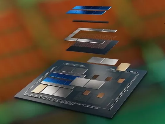
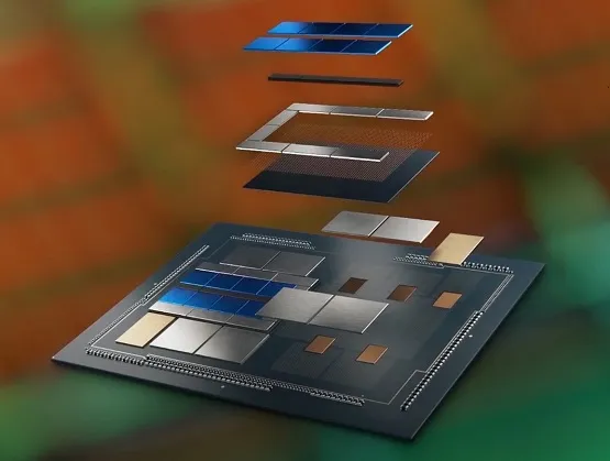
As monolithic scaling slows down, the semiconductor industry is increasingly relying on advanced packaging technologies to extend Moore’s law through heterogeneous integration. Higher on-package bandwidth, improved yield resiliency and the need to integrate diverse IP from multiple foundries are driving demand for advanced packaging technologies that address these issues but introduce challenges of their own such as efficient power delivery to all the different domains in a heterogeneous system. SEMI spoke with Kaladhar Radhakrishnan, Intel Fellow at Intel, about heterogeneous system integration trends and new developments in the semiconductor industry. Radhakrishnan shared his views ahead of his keynote at the SEMI Connecting Heterogeneous Systems Summit, 1-3 September 2021, an online event. Join the summit to meet experts from Intel and other key industry influencers. Registration is open. SEMI: What is driving the adoption of electronics and semiconductor devices nowadays and why is the development of new and innovative technologies important? Radhakrishnan: We are living in an increasingly data-driven world where devices have become an integral part of our lives. A recent study estimated that in the United States alone, 13.6 connected devices per capita consume an average of 300 gigabytes worth of data every month. In the workplace, COVID-19 has driven fundamental business changes that has sped up the adoption of digital technologies such as virtual conferencing, remote work, and e-commerce. Organizations are realizing that a high-quality video conference can be an adequate substitute for many in-person meetings. As a result, businesses are accelerating the digital transformation in order to adapt and thrive in this new environment. Five decades of sustained exponential growth in semiconductor performance has conditioned the average digital consumer to expect more from their devices. However, there are some headwinds ahead as traditional scaling slows down and power density rises. Because consumers and businesses are now generating data at a faster rate than they can consume it, technologists need to scale compute, storage, and bandwidth even faster to keep pace. Without investments in research and development of new and innovative technologies to address these challenges, the full potential of this data will go unrealized. SEMI: What forces are heightening the importance of heterogeneous system integration? What are the implications for increased on-package bandwidth, improved yield resiliency and the need to integrate diverse IP from multiple foundries? Radhakrishnan: The semiconductor industry increased transistor density and scaled performance through classical Dennard scaling until the turn of the century. By then, the gate oxide thickness had scaled down to atomic dimensions and the exponential increase in sub-threshold leakage signaled the end of scaling through traditional methods. Since that time, the chip industry has been relying on innovations in transistor materials and structures such as high-k metal gate, strained silicon, and FinFETs to keep pace with Moore’s law. However, this alone will not be sufficient to continue scaling and the industry needs to explore other vectors to augment improvements in transistor technology. Heterogeneous integration through advanced packaging is one key technology that can help drive these gains. Technologies like Foveros can enable device density scaling by creating a 3D stack of multiple die using high-density interconnects. Heterogeneous integration enables chipmakers to move from a monolithic system designed on a single large chip to a heterogeneous system comprised of a number of smaller chiplets. The main benefit of using smaller chiplets is that they improve yield and enable application based customization of the foundry processes. However, if the disaggregation to smaller chiplets is not accompanied by an increase in on-package bandwidth, the power and performance penalties associated with chiplet-to-chiplet communication will hobble system performance. This is why advanced packaging technologies that improve die-to-die communication are key enablers for heterogeneous integration. SEMI: What are some of the key technology challenges in developing heterogeneous systems? Radhakrishnan: The obvious challenge that most people focus on is the need for improved on-package bandwidth. However, as we rely on 3D stacking to continue device scaling at the package level, it is important to comprehend power delivery and thermal challenges as well. Power to the top die has to be delivered through TSVs on the bottom die, which not only adds resistance but also reduces the useful area available on the bottom die. This problem is further exacerbated when we stack more than two die. Excessive noise on the power delivery network can cause timing issues that limit the maximum operating frequency of the transistor. Similarly, when we stack multiple die, we must take into account associated thermal challenges. For example, each interface of the multi-die stack adds thermal resistance, which makes it harder to cool the chips at the bottom. SEMI: What are some of the key global market trends that driving demand for heterogeneous and system-level integration? Radhakrishnan: The number of artificial intelligence (AI) and machine learning applications have grown dramatically due to their ability to solve highly complex problems across a wide range of segments. AI and machine learning models require more memory bandwidth and compute capabilities that are difficult to achieve without some form of heterogeneous integration. Another market trend driving demand for heterogeneous integration is the increasing reliance on custom hardware accelerators. To combat the slowdown in frequency scaling and single-core performance, we have moved to multi-core architectures by tackling the inherent parallelism in our workloads. However, Amdahl’s law tells us that such an approach will hit a bottleneck when we reach the limits of the serial portion of the workload. As these constraints slow the performance of general-purpose processors, the reliance on custom hardware accelerators to boost performance for specific workloads is growing. Heterogeneous integration at the system level with a combination of CPUs, GPUs, FPGAs and other accelerators can optimize system power and performance. SEMI: What solutions is Intel developing to address these market needs? Radhakrishnan: Intel is actively involved in the development of the industry ecosystem for heterogeneous integration. We have developed a number of innovative advanced packaging solutions such as the EMIB and Foveros that are used in products today. Intel is also developing the next generation of advanced packaging technologies, Foveros Omni and Foveros Direct, which will dramatically scale the IO density by using direct Cu-Cu bonding technology. Foveros Omni is a crucial building block technology to enable high-voltage power conversion on the package for efficient power delivery. Intel is uniquely positioned to predict the design needs for future systems and deploy its resources to develop the technology building blocks needed to continue performance scaling. Our IDM 2.0 strategy enables us to leverage our leadership in packaging technologies to design the best products and use the best IP to deliver leading products across a broad range of categories. SEMI: What do you expect from your participation at SEMI Connecting Heterogeneous Systems Summit? Radhakrishnan: I’m hoping to shed some light on some of the new technologies we have been developing at Intel to enable heterogeneous system integration. I also want to bring awareness to the power-related challenges we are facing with heterogeneous systems. I also look forward to listening to what other industry leaders have to say on the topic. Kaladhar Radhakrishnan is an Intel Fellow and a Power Delivery Architect with the Technology Development group at Intel. He plays a significant role in shaping and driving power delivery technologies for Intel microprocessors. His areas of expertise include integrated voltage regulators, advanced packaging and passives technologies. Kaladhar is a two-time recipient of the Intel Achievement Award, the highest Intel honor an individual or small team can receive. He has authored four book chapters, over 40 technical papers in peer-reviewed journals, and has been awarded 35 U.S. patents. He has also served as an adjunct professor at Arizona State University. Kaladhar joined Intel in 2000 soon after receiving his Ph.D. in Electrical Engineering from the University of Illinois at Urbana-Champaign. Serena Brischetto is senior manager of marketing and communications at SEMI Europe.
Read More
As we pass the work-from-home one-year mark, most of us still work remotely and will do so for the foreseeable future. As live trade shows and technical conferences were cancelled one after the other, virtual events became the norm. And, teleconferencing became a way of life. While possibly overstating our role, we have the semiconductor industry – from system design through manufacturing and system integration – to thank for a long history of achievement that made the transition to working remotely relatively seamless and straightforward. The shift, in some cases, took some time to sort out as we set up a workable home office, moved to video conferencing with intermittent connections and settled into a routine. Nonetheless, many of us became more productive and, in some cases, even too productive. Each spoke in the global electronic products hub contributed through creativity and innovation with a pinch of ingenuity and grit. Of course, we could have worked remotely 10 years ago, but not nearly as efficiently. Over the last 10 years, the economy moved to the cloud, producing new opportunities across the global market. Many of these opportunities were made possible by the electronic system supply chain and combination of semiconductor technology, electronic product innovation and people who figured how to leverage it with software platforms to tie it together. Zoom, one of our teleconferencing lifelines, is a good example, as are Netflix, our ongoing source of entertainment, and Roblox, a platform to build games. Facebook, Twitter, LinkedIn and the like sourced the news for us and kept us in touch. Amazon delivered our online purchases and GrubHub brought us our takeout dinners. All rely on cloud computing with thanks to the semiconductor industry. Another great example are data centers powered by semiconductors and the amount of data they processed last year. According to International Data Corporation (IDC), 64.2 zettabyte (ZB) of data was created or replicated due to the dramatic increase in the number of people working, learning and entertaining themselves from home. (Its revised model for global data creation and replication predicts the CAGR will grow to 23% over the 2020-2025 forecast period, a sure bet that the semiconductor industry will address ways to manage the growth, possibly through new AI chips.) Our connectivity is driven by smartphones optimized for low power and the performance of more complex chips. Over the last 10 years, design tools have been enhanced and new methodologies have been introduced to respond to the needs of the increasing complex chips for applications that demand high bandwidth, low latency and reduced power consumption and area. Manufacturing is retooling for higher automation under smart manufacturing initiatives and packaging is even more sophisticated with increasing integration and the 2.5D and 3D packaging rollouts. Let’s take stock of our success. The semiconductor industry has a storied tradition of breakthrough technology since its inception. The consumer electronic product craze started when the first PCs were rolled out in 1971, notes the Computer History Museum. Primitive laptops that followed in 1986 gave way to notebooks in 2007 and the ubiquitous smartphone in 2002 – and the rocket fuel for much of this was the buildout of computer networks, hyperscale datacenters and the cloud. Nothing’s been the same since. The next time we turn on our laptop, click on the link for the latest teleconference from our remote home office in comfortable sweats sitting in our ergonomic chair, let’s take a minute to acknowledge our industry’s grand achievement. And, thank one and all for their contribution and consider what’s coming next. About the Author Robert (Bob) Smith is Executive Director of the ESD Alliance, a SEMI Strategic Association Partner. He is responsible for the management and operations of the ESD Alliance, an international association of companies providing goods and services throughout the semiconductor design ecosystem.
Read More
Emerging applications powered by 5G and artificial intelligence (AI) are expected to be a boon to the semiconductor industry, but only once chipmakers overcome a key challenge: Architecting chips that meet the exacting performance, power consumption, size and cost requirements of devices for mid- to high-end applications. One technology – heterogeneous integration – promises to meet these demands and help drive future leaps in semiconductor innovation in the post-Moore era. To help the industry better grasp the technology challenges and business opportunities associated with deploying highly integrated chip and packaging technologies, SEMI and AI on Chip Taiwan Alliance recently gathered industry leaders from organizations including ASE, Unimicron, Dialog Semiconductor, Cadence and AITA to discuss technology trends and the vital importance of building a cross-industry exchange platform to advance next-generation manufacturing processes critical to heterogeneous integration. Following are key takeaways from the forum, Heterogeneous Integration Enables 5G and AI. Overcoming Heterogeneous Integration Technology Challenges Key to Advances in Taiwan High-End Semiconductor Manufacturing The introduction of the Heterogeneous Integration Roadmap (HIR) by the International Technology Roadmap for Semiconductors team in 2016 was an important first step, Dr. C.P. Hung, Vice President of ASE Group, noted in his opening remarks. The HIR is designed to stimulate pre-competitive collaboration to advance heterogeneous integration technology development and accelerate electronics innovation. The roadmap provides a long-term vision for the electronics industry, identifying future technology requirements and potential solutions. Today, the HIR working group focuses on high-performance computing (HPC), 5G and other leading-edge technologies.Dr. Hung predicted that heterogenous integration will reshape traditional collaborations between the semiconductor ecosystem and supply chain in order to clear I/O bottlenecks that hamstring high-performance applications. The retooled industry connections will also need to enable high I/O pin counts, ultra-thin devices, and high-frequency signal shields. In an important step forward, the chip industry today is developing a platform that enhances wafer-level advanced packaging services and deepens cooperation with Oversea Assembly and Testing (OSAT) and substrate supply chain partners. Overcoming the current limits of IC substrates – the connection between IC chips the PCB – is one key for heterogeneous integration technology to flourish, said Dr. Yu-Hua Chen, Vice President, Carrier SBU, RD Division of Unimicron. He noted that the industry must tackle limits to PCB thickness, substrate density, fine pitch and automation to meet the needs of high-end packaging customers. Another barrier the industry must be surmounted is to make the currently inscrutable confidentiality requirements for patents of foreign materials – key to improving chip yields – easier to access and understand for substrate engineers. Chen said partnerships across the entire industry will be necessary to break through this and other technology breakthroughs. Supply Chain and Cross-Border Ecosystem to Strengthen Partnerships for Further DevelopmentTaiwan has long invested heavily in advancing semiconductor manufacturing and application engineering technologies to become a top global chipmaking hub and, in the process, has been behind significant leaps in optimizing chip functionality, said Leroy Liu, General Manager, Asia Headquarters, of Dialog Semiconductor (Germany). With its semiconductor manufacturing prowess, Taiwan can also play a central role in maturing advanced heterogeneous integration packaging technology while managing development costs by partnering with its international supply chain community to overcome technical challenges more effectively, Liu said. The region can also help forge partnerships, even among competitors, to build the ecosystem essential for heterogeneous integration technology to shine.EDA tools will be critical in understanding and resolving heterogeneous integration technical issues since IC substrate, packaging and chip design all pose interdisciplinary engineering challenges, said Julian Sun, Product Marketing Director at Cadence. To help the industry navigate these challenges, Cadence has launched intelligent system design products – solutions that address a wide range of design problems with semiconductor nanometers, micrometers on packaging and testing, and PCB level micro/millimeters to Pin/Pitch, I/O models, and thermals and electricity. By supporting various technical designs, Cadence helps customers shorten the design cycle to strengthen design quality and reduce costs.Sun also pointed to the vital importance of overcoming the significant challenge of designing silicon interposers for heterogeneous integration. Today’s EDA tools are capable of optimizing the design of complex structures including 5GAiP and HBM and are instrumental in aiding Taiwan’s semiconductor ecosystem players to quickly adapt to shifts in the evolving heterogeneous integration market.Heterogeneous Integration Enables 5G and AI speakers (L-R): Julian Sun, Product Marketing Director at Cadence, Dr. Yu-Hua Chen, Vice President, Carrier SBU, RD Division of Unimicron, Dr. C.P. Hung, Vice President of ASE Group, Leroy Liu, General Manager, Asia Headquarters, of Dialog Semiconductor (Germany), Dr. Shih-Chieh Chang, AITA Executive Secretary Designing AI chips is particularly difficult as semiconductor makers struggle with high costs and low yields, said Dr. Shih-Chieh Chang, AITA’s Executive Secretary. That’s why the chip industry now uses FPGAs for small-volume production of AI chips, which makes it easier to improve manufacturing yield through redundant design. For its part, AITA has formed a special interest group (SIG) to help form connections among the chip industry, academia and research institutes. The association’s goal is to build a platform for mass production of AI chips.To get involved in SEMI Taiwan Heterogeneous Integration related events, please contact Ula Huang, outreach senior specialist, at [email protected] Fang is a coordinator and Ashley Huang is a specialist in marketing and public relations at SEMI Taiwan.
Read More
Post-Conference Report: SEMI Heterogeneous Integration SummitDemand for high-performance computing (HPC) chips is exploding. These super-speedy chips are critical for data centers and cloud computing infrastructures to support new performance-hungry technologies such as artificial intelligence (AI) and 5G. The challenge is for the devices and their multi-core architectures to couple high bandwidth density with low latency and high energy efficiency. Heterogenous integration offers a potential answer as an advanced packaging technology designed to meet these skyrocketing performance demands on HPC chips and open the door to a whole new world of 3D integrated circuits (ICs).So important are 3D ICs that Intel and TSMC representatives speaking at the recent Heterogeneous Integration Summit hosted by SEMI Taiwan in Taipei declared that the packaging technology will all but dictate the future of the industry. All told, 12 speakers from government, academia and a broad range of leading international companies from sectors including advanced packaging, design, manufacturing, silicon photonics, equipment and materials shared forward-looking strategies, the latest technologies and potential heterogeneous integration market opportunities. Koushik Banerjee, vice president, TMG, Assembly, and Test Technology Integration, at Intel pointed out that using heterogeneous integration for a single SiP (system-in-package) will deliver what the industry has long wanted by enabling multiple process nodes, more diverse silicon IP (intellectual property) and chip functionality, and chips that pair low energy with high frequency. Intel plans to announce its first Forveros 3D packaging product combining a 10nm HPC chiplet with a low-energy 22nm base die and stacked with memory on top. When asked about the future of advanced packaging technology, Banerjee said it will be very much about the combination of Foveros and its very own Embedded Multi-Die Interconnect Bridge (EMIB).For its part, TSMC, will continue to upgrade its CoWoS (Chip-on-Wafer-on-Substrate), InFO (Integrated Fan-out) and other 2.5D IC production solutions while developing 3D chip stacking technology such as SoIC and WoW (wafer-on-wafer). TSMC is ushering in a new age of 3D IC packaging, said Marvin Liao, Vice President, Backend Technology and Service Division, at TSMC. The company’s SoIC is based on Chip-on-Wafer concept, with the flexibility to support one-to-many or different process nodes, whereas its WoW integrates two wafers with solid yields that could be used for products of the same size or manufactured with mature process technology.Speakers also included representatives from ATOTECH, Lam Research, SPIL, Sigurd, Cadence, Grand Process Technology, ITRI (Industrial Technology Research Institute), Industrial Development Bureau, and Lee San-Liang, Distinguished Professor, Department of Electronic and Computer Engineering at National Taiwan University of Science and Technology all shared their perspectives on equipment, materials, and testing and how different industry value chains might contribute to the development of heterogeneous integration technology.Expected to be a key driver of the next wave of semiconductors, heterogeneous integration and related technologies – including 3D IC, FOWLP (Fan-out wafer-level packaging) / FOPLP (Fan-out panel-level packaging), silicon photonics, Micro LED, compound semiconductor, automated optical inspection and SLT (system level testing) – will be a key focus at SEMICON Taiwan 2019, September 18 to 20 in Taipei. The Heterogeneous Integration Innovation Zone – along with featured international programs such as SiP Global Summit, Strategic Materials Conference, the Smart Data Summit and the Smart Automotive Summit – will gather key industry players to reveal the latest technology breakthroughs and market trends.Emmy Yi is a senior marketing specialist at SEMI Taiwan.
Read More
SEMI met with Martin Schrems, director of Strategy and Business Development at AT S AG, to discuss Fan-Out technology trends ahead of SEMI 3D Systems Summit in Dresden, Germany.SEMI: What are the AT S AG mission and vision and your role within the company?Schrems: AT S AG is evolving from a pure PCB manufacturer towards an interconnect solution provider. We can clearly see a continued trend towards miniaturization and modularization by (3D) integration of components such as integrated circuits and passives. Module sizes tend to increase by integrating more functions and system-level requirements. As a PCB maker, we have served such system-level requirements for a long time. Further integration offers opportunities to embed components in PCBs or substrates, offer layout and simulation services, as well as provide assembly and test services depending on specific customer requirements. As director of Strategy and Business Development, I work with my colleagues in AT S, customers, and partners across the industry towards understanding and leveraging this major transformation in the electronics industry.SEMI: What project are you currently working on that you think will make a difference in 2019?Schrems: There are number of very exciting projects, many of them already involving AT S contributions to module integration. Some of these projects involve key customers directly. We see exciting opportunities for integration of larger multi-function modules by combining PCB, substrate, and embedding core competences.SEMI: The focus of your presentation at the 3D Systems Summit will be on "Fan-Out System-in-Board technology enabling module and system-level integration.” What do you see as the key trend in this area?Schrems: Fan-Out technologies are used to distribute I/O pad connections of nanoCMOS ICs over a larger area. This relaxes bump pitch and feature size requirements for subsequent system-level PCB interconnects. In some cases, Fan-Out layers already provide a substitute to currently used Flip-Chip substrates. Well-known examples are Fan-Out packages for application processors for smartphones. There is definitely a trend in the market towards Fan-Out for high-end processor applications. Advantages of such Fan-Out packages are shorter electrical connections and a reduced thickness.However, one weakness of current Fan-Out packages is that only a limited number of components can be integrated due to mechanical stability challenges – a barrier to further component integration in larger modules. Currently, the only way to integrate more components is to use laminate-based PCBs and substrates with conventional Surface Mount Technology. Recent proposals like our “Fan-Out System-in-Board” (FO-SiBTM) technology are expected to provide an alternative Fan-Out packaging option at the board-level in the future.SEMI: Please elaborate. Schrems: Fan-Out capability and integration of more components – typically up to the 100 and more needed for electronics integration at system level – can be achieved simultaneously by combining technologies from the PCB and the packaging world. PCB laminates such as glass particles and organic materials provide mechanical stability for large boards. The recent introduction of substrate-like PCBs (mSAP) has already paved the way to cover applications that were reserved for substrates and classical packaging in the past.With FO-SiBTM technology, we have taken it a step further and offer the option to integrate SAP substrate layers onto the PCB with lines/spaces below 10µm. FO-SiBTM makes it possible to directly contact nanoCMOS chips on PCBs without any intermediate substrates. Further adding Cu pillar technology at panel level will enable Fan-Out structures even for surface-mounted components, making recent R D on panel-level Cu pillar technology very important. Through joint R D, we can drive progress in the industry to further enable cost-effective heterogeneous 3D integration.SEMI: What are your expectations for the 3D Systems Summit in Dresden, and why do you recommend your members and other industry leaders to attend?Schrems: The 3D summit is the high-level conference where key electronics industry players discuss major heterogeneous integration trends. Therefore, we very much appreciate the opportunities to exchange ideas across the supply chain including users, developers of integrated electronics hardware and tool manufacturers. Serena Brischetto is a marketing and communications manager at SEMI Europe.
Read More
New SEMI Taiwan Testing Committee to strengthen the last line of defense to ensure the reliability of advanced semiconductor applications.Mobile, high-performance computing (HPC), automotive, and IoT – the four future growth drivers of semiconductor industry, plus the additional boost from artificial intelligence (AI) and 5G – will spur exponential demand for multi-function and high-performance chips. Today, a 3D IC semiconductor structure is beginning to integrate multiple chips to extend functionality and performance, making heterogeneous integration an irreversible trend. As the number of chips integrated in a single package increases, the structural complexity also rises. Not only will this make identifying chip defects harder, but the compatibility and interconnection between components will also introduce uncertainties that can undermine the reliability of the final ICs. Add to these challenges the need for tight cost control and a faster time to market, and it’s clear that semiconductor testing requires disruptive, innovative change. Traditional final-product testing focusing on finished components is now giving way to wafer- and system-level testing.In addition, the traditional notion of design for testing, an approach that enhances testing controllability and observability, is now coupled with the imperative to test for design, which emphasizes drawing analytics insights from collected test data to help reduce design errors and shorten development cycles. Going forward, the relationship among design, manufacturing, packaging, and testing will no longer be un-directional. Instead, it will be a cycle of continuous improvement.This paradigm shift in semiconductor testing, however, will also create a need for new industry standards and regulations, elevate visibility and security levels for shared data, require the optimization of testing time and costs, and lead to a shortage of testing professionals. Solving all these issues will require a joint effort by the industry and academia. "With leading technologies and $4.7 billion in market value, Taiwan still holds the top spot in global semiconductor testing market," said Terry Tsao, President of SEMI Taiwan. "When testing extends beyond the manufacturing process, it can play a critical role in ensuring quality throughout the entire life cycle from design and manufacturing to system integration while maintaining effective controls on development costs and schedules. Taiwan's semiconductor industry is in dire need of a common testing platform to enable the cross-disciplinary collaboration necessary for technical breakthroughs."The SEMI Taiwan Testing Committee was formed to meet that need, gathering testing experts and academics from MediaTek, Intel, NXP Semiconductors, TSMC, UMC, ASE Technology, SPIL, KYEC, Teradyne, Advantest, FormFactor, MJC, Synopsys, Cadence, Mentor, and National Tsing Hua University to collaborate in building a complete testing ecosystem. The committee addresses common technical challenges faced by the industry and cultivates next-generation testing professionals to enable Taiwan to maintain its global leadership in semiconductor testing.The SEMI Taiwan Testing Platform spans communities, expositions, programs, events, networking, business matching, advocacy, and market and technology insights. For more information about the SEMI Taiwan Testing platform, please contact Elaine Lee ([email protected]) or Ana Li ([email protected]). Emmy Yi is a marketing specialist at SEMI Taiwan.
Read More