downloadGroupGroupnoun_press release_995423_000000 copyGroupnoun_Feed_96767_000000Group 19noun_pictures_1817522_000000Member company iconResource item iconStore item iconGroup 19Group 19noun_Photo_2085192_000000 Copynoun_presentation_2096081_000000Group 19Group Copy 7noun_webinar_692730_000000Path
Skip to main content
Default Banner Image

Industry 4.0

SEMI is pleased to welcome Singapore-based UTAC Holdings Ltd., formed nearly 50 years ago, as a new member. UTAC is a leading independent provider of assembly and test services for a broad range of semiconductor chips, offering a full range of semiconductor assembly and test services across analog, mixed-signal and logic, and memory. Its customers are primarily fabless companies, integrated device manufacturers and wafer foundries. The company has production facilities in Singapore, Thailand, China, Indonesia and Malaysia as well as sales offices in five regions: the United States, Japan, China, Taiwan, the rest of Asia and Europe.I recently spoke with Dr. Nathapong Suthiwongsunthorn, Vice President and General Manager of UTAC Thailand, about UTAC’s smart manufacturing advances, the company’s role in the semiconductor industry’s transformation, and the industry outlook for Thailand over the next year.Ng: How does UTAC Thailand complement your other facilities?Dr. Nathapong: As one of the world’s largest producers of quad-flat-no-leads (QFN), UTAC Thailand has significant capability in assembly and test of advanced leadframe products including power products such as Cu Clip packages as well as MEMS products. We also serve top global IDMs and have the largest share of assembly and test for the automotive market among all UTAC operations. UTAC’s other facilities have expertise in wafer-level packages and system-in-a-package and serves the communication and consumer market not only for IDMs but also for the fabless and foundry companies. The Thailand factory nicely complements the other UTAC facilities both from the standpoint of operational and marketing diversity. Ng: UTAC Holdings Ltd. announced in August this year that it has completed its sale to Wise Road Capital, a global private equity firm. Will this in any way change the operation and business strategy of UTAC Thailand?Dr. Nathapong: I don’t believe it will change the way we operate. However, the acquisition is very positive for us from a financial perspective. With the benefit of significantly reduced debt and interest expenses, we will be able to expand our business to grow with and hopefully beyond the semiconductor market. Ng: To what extent has UTAC adopted smart manufacturing?Dr. Nathapong: UTAC Thailand is leading the way in terms of automation, smart manufacturing and Industry 4.0 with our in-house automation team and unique expertise. For example, we have built our own inspection equipment that is much faster and cheaper than what is commercially available. We also working on many programs such as mobile robot, AGV, auto inspection and office automation to help drive greater production efficiency. We are replicating our manufacturing advances and fanning them out to other UTAC facilities.UTAC Thailand Ng: What are some of the challenges you face in pushing for the industrial transformation in Thailand?Dr. Nathapong: I think the key challenge is to find skilled engineers who can perform hardware- and software-related tasks critical to the industrial transformation. But frankly, we have done a good job in managing this challenge by hiring very smart people, providing them with the required in-house training, and using outside training for new recruits as necessary. We have developed partnerships with capable vendors in this regard as well.Ng: What are the key differentiating elements (e.g. talent, tax, technology, trade, EHS) in Thailand that have been instrumental in supporting the E E ecosystem?Dr. Nathapong: There are two key differentiating elements for us. Firstly, UTAC has been around for over 47 years and is very well-established in Thailand with a positive reputation as an employer. This makes hiring talented people relatively easy. Secondly, and perhaps more importantly, the nature of the Thai people and also the benefits the company provides make it relatively painless to retain key employees. I also believe that we have a significant number of engineers available in Thailand. Finally, labour costs in Thailand are still very reasonable and stable. So we are able to acquire talent at a very competitive rate compared to other countries. Ng: What is the industry outlook for E E industry in Thailand over the next year?Dr. Nathapong: Surprisingly, the current sad predicament of COVID-19 has shown no negative impact for the global semiconductor industry – people seem to be buying more electronics with the lockdown. Our outlook for the Thailand’s E E industry is similarly very positive. Most semiconductor companies including UTAC see significant growth this year and I hope it will continue.Ng: With the recent semiconductor geopolitical and trade tensions, are more customers moving their business to Thailand?Dr. Nathapong: I believe so. We do see some of our key customers move manufacturing out of China and into Thailand. The relocations help them offset or avoid any potential fallout from current geopolitical tensions.Ng: In what areas do you think SEMI Southeast Asia can play a role to help our members companies in Thailand like UTAC?Dr. Nathapong: The semiconductor industry has been in Thailand for a long time. In fact, UTAC Thailand is 47 years old this year! However, I feel that Thailand never really worked with a strong establishment organization like SEMI that can connect various companies together to help drive innovation. I think SEMI Southeast Asia can truly help Thailand to move up to the next level of providing semiconductor solutions globally. We welcome SEMI Southeast Asia’s help in this regard.About Dr. Nathapong SuthiwongsunthornDr. Nathapong Suthiwongsunthorn joined UTAC in 2009 and is currently General Manager of UTAC Thailand, UTAC’s largest operation site. Before taking over the management of Thailand operations, he was Vice President of Research and Development, running UTAC’s global R D group. Dr. Nathapong has more than 20 years of experience in the semiconductor industry. He holds more than 40 international patents and publications in wafer-level and advanced packaging.Prior to joining UTAC, Dr. Nathapong held several key leadership positions in research and development at Schott, STATS ChipPAC and Infineon. Dr. Nathapong has a Ph.D. in Electronics Engineering from Oxford Brookes University, England.Bee Bee Ng is president of SEMI Southeast Asia.
Read More
I recently spoke with Chan Pin CHONG, Executive Vice President and General Manager of Products and Solutions at Kulicke Soffa, about how smart manufacturing is driving new production efficiencies in the semiconductor industry. During our conversation, he also provided practical steps for factory operators to follow in evaluating their smart manufacturing needs in order to ensure successful implementation and discussed the potential payoffs. Based in Singapore, Kulicke Soffa is a leading global provider of ball bonding, advanced packaging, wedge bonding, and electronic assembly equipment for the semiconductor, power and automotive industries.Ng: Industry 4.0 and smart manufacturing are critical to the growth of the semiconductor industry. What does the smart manufacturing movement mean to you or Kulicke Soffa?Chong: The future of smart manufacturing is the vision of building a digital connected factory to drive new manufacturing efficiencies by combining physical and cyber technologies. Industry 4.0 integrates discrete systems and harnesses the power of large volumes of data to move towards greater automation.At K S, we define smart manufacturing across the following four key areas embedded in our roadmap for all K S products, from wire bonders and advance placement tools to pick and place machines: Interoperability – This is about machines, devices and sensors connecting to each other. In fact, the very basis of smart manufacturing is that all devices are connected. Information transparency – Through simulation, various artificial intelligence (AI) tools use contextual information to emulate the actual world. Technical assistance – Robots or machines support humans in making decisions or solving problems. Autonomous decision-making – This is our vision that robots or machines can learn from machines to make decisions on their own. Ng: Please elaborate on some of these areas and how they’re the relevant to smart manufacturing. Chong: The need for machines, devices and people to communicate with each other forms the basis of connectivity, the idea of all machines communicating with each other or a host. Connectivity protocols now in place for machine-to-machine connectivity include SEMA, SECS/GEM, SEMI-ELS and IPC-CFX. Machine technology uses various sensing technologies. For example, for a pick and place machine such as SMT platform on K S Hybrid, the algorithm to recognize and align processes is part of the sensor needed in each machine before to can process and add thousands of components to the substrate or panel. In a wire bonder, the ultrasonics or EFO signal can provide some form of sensing technology for a machine to detect process conditions. Importantly, these sensing technologies can be used to collect feedback for process improvements.One example of how K S machines are connected to the host is our use of an intermediate server or host named KNeXt to connects to all assembly equipment in the fab. The equipment can then, in turn, connect to an external secured cloud or K S Global Cloud.Ng: What are the objectives for smart manufacturing?Chong: The ultimate goal is to achieve higher factory productivity or better OEE (Overall Equipment Effectiveness) by improving machine yields, productivity and efficiency. The key is to leverage AI, 5G, the Internet of Things (Iot) and other industry 4.0 technologies to drive automation and process improvements. Ultimately, each factory must meet productivity, yield and cost goals. Smart manufacturing enables factory operators to meet these goals. That is the focus of smart manufacturing.Ng: What is the biggest potential benefit of smart manufacturing?Chong: Smart manufacturing uses data to predict outcomes of a process step or machine operation. Once data is available in the global cloud, analytics can start to build data sets to run statistical modelling and examine factory operation trends. We can also use the data to identify past machine behaviors in order anticipate outcomes, including undesirable ones that we can then prevent.In the SMT example, if we can systematically examine days or weeks of historical performance, we can plot some statistical variations in the process specifically to a pick or placer or a robot and anticipate or avoid problems. However, all sensors must be in place in the bond head or the robot so that we can detect changes or variations in the robot’s movements.Kulicke Soffa smart manufacturing facility Ng: What are some recent factory improvements smart manufacturing has enabled? Chong: Kulicke Soffa has contributed to the hierarchical architecture of the smart factory and key technologies. COVID-19 is driving demand for greater factory connectivity, and K S offers solutions that are key to remote management and full control of smart equipment from a central control and embedding Internet of Things (IoT), big data, cloud computing and sensors in manufacturing. Using these technologies, a small smart factory can be remotely operated and managed.With COVID-19 limiting air travel around the world and access to support engineers, the need has grown for remote machine access to reduce the downtime per machine. Remote factory access enables off-site engineers to remotely identify and diagnose machine problems.Ng: What are barriers to faster adoption of smart factories?Chong: While most smart factories are capable of network connectivity and data collection, a key challenge is the lack of a business model for smart factories and smart equipment. Most factories must justify major capital investments by demonstrating ROI (Return of investments) potential. Capital improvements for every factory usually take several years to implement and are based on a complex business model. Factory connectivity requires substantial investments and years to implement. The same is true of the cloud infrastructure buildouts necessary to generate big data and meaningful analytics. The executive mandate for factory management to install capability usually calls for specific business targets in the planning stage.Another longstanding barrier to entry is the lack of compatibility of existing tools with new factory protocols, raising the question of whether the cost of replacing legacy tools justifies the need for a smart factory. If new factory investment is required for the latest tools to support the production of new products, the ROI will be much easier to justify.Ng: How is AI is important in smart manufacturing?Chong: AI interprets and learn from data to perform tasks and meet specific goals. Good examples of AI implementations include Amazon’s Siri and Alexa voice-command devices and self-driving cars being developed by Google and Tesla.At K S, over the years we’ve implemented AI in our smart wire bonders to reduce human intervention in our ProCu-7, PSP-2, ProCu Loop 2, Pro Bump and overhang processes.Thanks to AI, with senses of signals from the bonder, we can reduce the amount of parameters that an engineer or technician have to do trial and error. With on bonder metrology, PBI, loop height, wire sway features, AI allows us to measure process efficiency and provide feedback.Over several years of AI development, we have leveraged the technology to monitor machines and provide real-time performance feedback in order to provide better closed loop control such as short tail recovery in our bonder process. We can also use the data to predict machine behavior, monitor its health and track maintenance. Ultimately, AI enables fabs to improve manufacturing efficiency, productivity, yields and device quality.Ng: What’s an example of how AI has solved your manufacturing equipment problems?Chong: We’ve used AI to set RPM (real time monitor) limits, identify defective P-parts and monitor various conditions such as wire size and capillaries. These types of cases can arise in any manufacturing environment as humans make process mistakes or use the wrong part for a machine. With AI, we can prevent these problems and reduce the risk of further material lost from the wire bonding process.Ng: What advice do you have for factories looking to implement smart manufacturing systems?Chong: To build a smart factory, start by focusing on a clear set of business objectives and how smart manufacturing will help minimize or eliminate current factory inefficiencies. In other words, start with the end in mind – the problems that needs to be solved and the business goals – and identify the information you need to demonstrate ROI. Do you need to resolve, automate or improve processes or just to be more efficient? Before investing millions or billions of dollars to build a smart factory, identify those clear goals upfront. Then map out the particulars of implementation to avoid major problems around standards, protocols and connectivity.Bee Bee Ng is president of SEMI Southeast Asia.
Read More
The costs of production are typically based on labor and materials and define manufacturing expenses. But is this approach accurate enough? What about the cost of poor quality and lack of efficiency in production? How is the pandemic impacting semiconductor manufacturing and what can we expect from the future?SEMI recently spoke with Dr. Eyal Kaufman, founder and CEO of QualityLine, a Kiryat Gat, Israel-based provider of smart manufacturing analytics solution, about manufacturing controls and how to select the best data source to improve product quality and yield. Kaufmann provided a snapshot of current best practices used by the company to improve manufacturing efficiencies and product quality while reducing costs. He also discussed the COVID-19 pandemic’s impact on semiconductor smart manufacturing and how artificial intelligence (AI) can help keep factory workers safe.For additional insights on smart manufacturing, join the virtual SEMI Global Smart Manufacturing Conference, October 20 - 22, 2020. Registration is open.SEMI: Real manufacturing costs are calculated based on different aspects such as failures in production, repairs, products returned, scrap of components or late deliveries. Lack of quality and efficiency in manufacturing can undermine a business. How are you helping businesses overcome these challenges?Kaufman: To increase profit margins, it is essential to identify inefficiencies and what improvements to prioritize. Once manufacturing quality and efficiency deficiencies have been measured, the next step is to continuously collect manufacturing data in order to run the final cost analysis and use the analytics to improve the manufacturing process.Smart manufacturing makes it possible to detect anomalies in automated factories, improve production performance and increase profitability. Today, automated data are collected from every machine and piece of test equipment in the factory. Still, manufacturing data collection in many industries remains manual and expensive because of the time and human resources involved. A real-time analytics system can automatically collect all data sources and select the relevant data for analysis, which today is the most accurate and effective way of measuring and resolving quality and efficiency deficiencies.Data-driven decisions made by smart manufacturing reduce costs and improve manufacturing strategies, enabling factory operators to increase product quality, drive higher production capacity and enhance product design for manufacturability. Analytics solutions monitor shop floor operations accessing vendors and subcontractors’ products criterion to run root cause analysis. All those data will reduce the return rate of faulty products and accelerate return on investment. This is why we definitely need smart manufacturing technologies!SEMI: Data accumulated during the manufacturing process includes vital information about failures, anomalies and machine usability. What data are necessary to create the best analytics solution?Kaufman: Many companies today run data mapping and automatic creation of data capture. They often wonder if they need to use testing data, sensors data or product design data, or whether they should collect feedback from their customers and vendors. The best way to create an effective manufacturing analytics system is to use data sources such as: Feedback from customers (returned units, customers complaints, etc..) Testing data from automated test equipment and manual test activities Feedback from technicians repairing faulty units Analysis of testing processes done by vendors Sensors data Data from our ERP/MES systems Artificial intelligence enables any type and size of data structure, even accumulated data, to be automatically integrated and interpreted. AI-based analytics can also establish correlations between each manufacturing stage to help factory operators quickly conduct deep diagnostic and root cause analysis for problem solving and prevention – all while leaving intact a factory’s existing process, machinery and data output. Machine learning evaluates how a factory runs its database and puts all the information generated into an analytics solution that provides the know-how to continuously improve factory efficiency.SEMI: How do you select the best data source to improve manufacturing quality and yield? Kaufman: The accuracy and integrity of data accumulated in our manufacturing process is key to controlling and improving yield and quality while reducing manufacturing costs. Smart manufacturing is a technology-driven approach that uses digital and remote connected machinery to monitor the production process. The goal is to identify anomalies in manufacturing processes and leverage analytics to improve process yield and product quality.To select the relevant data, we collect each type and source of data that can improve the efficiency of a real manufacturing cell: Test data from Automated Testing Equipment Test data from Manual Testing Processes Analyses of repairing processes (failed units during the manufacturing process and units that were returned from customers) Once the data structure is collected, the next step is to turn it into actionable information in the manufacturing process. QualityLine smart manufacturing solutions provide a complete one-stop solution to interpret any manufacturing data structure. Our advanced manufacturing analytics solution detects quality and yield anomalies to reveal production line inefficiencies and opportunities to improve manufacturing quality and efficiency.SEMI: How would you describe your approach?Kaufman: Industry 4.0 in manufacturing claims to be the fourth generation of the industrial revolution. Advanced technologies like manufacturing intelligence and machine learning can efficiently achieve zero defects on manufacturing lines. Digital factories leverage technologies and methodologies including: Big data Self-optimization Self-configuration Self-diagnosis Cognitive and machine learning Smart manufacturing technologies enhance the manufacturing process by continuously collecting and analyzing data in real-time to achieve and maintain high quality performance. The goal is to achieve a significant increase in efficiency and yield while reducing waste and inefficiency.Until now, there has been no viable way to integrate all saved manufacturing data into a unified database. QualityLine advanced manufacturing analytics make it possible for any factory to become digital without installing new hardware, which can be expensive and require not only the extensive integration of existing data but investments in training. Our user-friendly solution integrates manufacturing data for industries with zero automation by first collecting and analyzing data from any type of manual test procedure and then integrated it into manufacturing analytics to improve efficiency.SEMI: Why are Pass/Fail criteria insufficient for controlling manufacturing yield and quality?Kaufman: Managing a mass manufacturing process is always a challenge because hundreds of tasks must be successfully completed before products can ship to customers. At QualityLine, we establish a test process for each stage of the production flow, from the incoming raw material to the final stage prior to the delivery of finished goods to the client. To prevent unexpected downtime incidents, waste and defective products, we collect and interpret every type of relevant data and turn it into meaningful information, setting up the following capabilities: Collection and interpretation of test and process data of each single unit and from each process and plant Automatic detection of quality and yield problems Accurate and quick root cause analysis process Automatic alerts to abnormal issues Prediction process potential and level of failures Measurement of key performance indicators Many manufacturers base their test criteria of each parameter on one key indicator – Pass or Fail. If the test result shows a Pass, then the unit is ready to move on to the next manufacturing stage. If the test result shows Fail, then the unit is sent to a technician for further analysis.A simple Pass or Fail criteria for product quality is far from sufficient since it provides little or no information about edge cases, where one or more of the technical parameters of the unit under test is only within its allowed tolerance. Edge cases may lead to unit failure during operation such as in extreme environments (cold, heat, humidity, electrical overload, impact, etc.). In fact, when running a mass manufacturing line, it is impossible to continuously digest all the detailed information collected from testing stations. Data is analyzed in detail only when a critical quality problem emerges and further analysis is required to understand the root cause.Information overload and the disregard of important parameters makes it hard to control the process and improve quality and yield. New technologies make fast and scalable data integration possible so data can be collected in real time to detect quality issues early, identify complex process disruptions to avoid delivery delays and ensure the best possible product for customers. Only by accurately analyzing data as actionable information can factory operators control the manufacturing quality process.SEMI: How has COVID-19 impacted the smart manufacturing market? How has your technology helped factories remain online?Kaufman: Smart manufacturing is playing a significant role by helping manufacturers overcome COVID-19 challenges such as workforce reductions, social distancing, drops in sales for some specific products and extreme pressure to cut operational costs.Manufacturing leaders turned to us for a solution to the challenges of maintaining efficient factory operations with a limited workforce and reduced number of operating hours. Filling factory orders with fewer people on the floor is a struggle. Digital factory technologies enable remote monitoring of operations to increase efficiency and capacity. We are helping our clients improve efficiency while reducing costs. Our remote monitoring technology can provide the operational visibility to floor managers and engineering teams who cannot go physically to the factories due to safety restrictions. With our advanced manufacturing analytics, they have full end-to-end visibility and can remotely diagnose and solve production line issues. During this critical time, we are proud to be improving remote monitoring solutions to help the industry withstand the pandemic. Some of our clients would have closed their factories otherwise. We’ve been working to integrate manufacturing data in factories that were previously unautomated to drive high automation levels. Integrating processes with existing factory data, regardless of customer’s protocols or automation level, is our great technology advantage.SEMI: How will manufacturing and its supply chains look after COVID-19?Kaufman: Smart manufacturing is currently a necessity. We collect and analyze data not only to improve quality but to reduce client returns of faulty products by 50% and reduce waste by 22%, both critical points. Manufacturing challenges will continue to accelerate advancements in technology and improve efficiency, safety and productivity as more factory operators incorporate real-time data analytics and artificial intelligence (AI). SEMI: Will suppliers continue to explore new avenues for smart manufacturing technologies and what are their growth opportunities?Kaufman: Yes, definitely. The sector has already changed, with COVID-19 bringing both opportunities and challenges. Industry leaders are facing new pressure, with sudden materials shortages, drops in demand and worker unavailability. The growth opportunities for manufacturing are likely to be digital, as already evident in the immediate response to the crisis. Industry 4.0 solutions will be crucial to increase end-to-end supply-chain transparency, automation and data integration. QualityLine manufacturing analytics have improved key manufacturing performance metrics. For example, based on customer feedback, we’ve increased production yield by 30%, saving some of our customers millions of dollars. Improvements like this can help suppliers withstand pandemics.Dr. Eyal Kaufman, Founder and CEO at QualityLine, has senior management experience and over 25 years of expertise in business development, marketing, finance, operations, engineering and quality management at leading industrial companies. Prior to QualityLine, he served as VP of Mobileye, Cardo Systems, and Medisim Ltd., as well as CEO of OnTheGo Systems. Eyal holds a Ph.D. from California Intercontinental University, an MBA from City University of New York and a BSc. from the Technion in Israel.The SEMI SMART Manufacturing Initiative is a global effort to promote awareness and interest about smart manufacturing with focus on delivering industry-recognized best-in-class programs and services to enable members to maximize product quality, productivity and cost improvements through smart manufacturing. Activities are focused on building out core capabilities to enable smart manufacturing across the microelectronics supply chain.MADEin4 is a consortium of 47 partners from 10 countries connecting the full range of supply chain: from semiconductor equipment manufacturers and system-integrating metrology companies to RTOS and key applications such as the automotive industry. The MADEin4 Project develops next generation metrology tools, machine learning methods and applications in support of Industry 4.0 high volume manufacturing in the semiconductor manufacturing industry.Serena Brischetto is a senior manager of marketing and communications at SEMI Europe.
Read More
Teck Khiong, WOI, senior manager of Factory Integration at Infineon Technologies Asia Pacific Pte Ltd, recently shared with me how the Infineon backend plant in Singapore has benefited from its journey to qualify for the lighthouse certification.WOI is driving Infinion smart manufacturing projects with a strong focus in the area of connect and control using IoT (Internet of Things) and analytics technologies. Ng: How did the Infineon backend plant in Singapore distinguish itself to qualify for lighthouse certification? WOI: The Infineon Singapore backend manufacturing plant is proud to be a Lighthouse Certified Smart Manufacturing site as part of the World Economic Forum’s (WEF) Fourth Industrial Revolution platform. Our Industry 4.0 (I4.0) implementation reduces labor costs by 30% and improves capital efficiency by 15%. We drove this successful digital transformation continuously investing in our people development and digital backbone.Of the many initiatives under our I4.0 Smart Factory platform, five were selected for WEF Lighthouse submission and certification. Digital foundation with integrated connectivity and workflow execution We implemented an Internet of Things (IoT) framework to connect machines to manufacturing system more than two years ago. The digitization of our Work-in-Progress (WIP) management systems provides full traceability and gives us better control of the four Ms (Man-Machine-Method-Material). Material handling and process automation We progressively deployed automated solutions starting six years ago using autonomous transport, robotic material management systems and automation of packing processes. This eliminated non-value touches in areas of WIP storage and retrieval. Advanced algorithms enabled WIP scheduling and dispatching As our product mix and volume grew in complexity, our advanced algorithms has enabled us to increase our machine uptime, thus reducing idle and set-up time. Manufacturing control tower Our control tower provides a real-time pulse of the entire manufacturing process, from machine efficiency to quality. The tower also improves data integrity and collaborative information sharing while issuing early-warning alerts that enable exception management and timely decisions. Running a global virtual factory Our Global Production Network deployments allows us to connect and manage a growing contract-manufacturing network in real time, with the same transparency, traceability and control as if the manufacturers are our internal sites.About Teck Khiong, WOITeck Khiong, WOI graduated from Loughborough University in the UK with a Master of Science degree in Computer Integrated Manufacturing (CIM). For more than 20 years he has delivered manufacturing IT solutions to global backend (assembly and test) semiconductor manufacturing, ranging from equipment, factory, process control, material handling automation and manufacturing execution systems (MES).
Read More
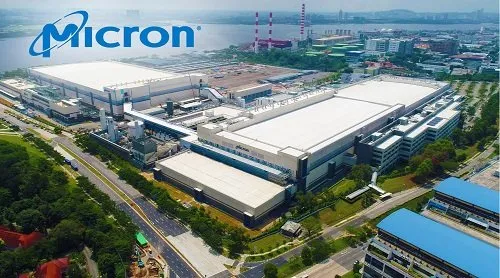
Making Strides TogetherKnowledge is power – especially when it is shared. This principle formed the foundation for Micron’s Go and See virtual visit of its Singapore manufacturing plant on 26 August 2020 as 27 companies including GLOBALFOUNDRIES, ST Microelectronics, Infineon, TEL, ViTrox , IBM, HP and UTAC joined the first-of-a-kind virtual factory visit. The chip industry powerhouses gathered to see how Micron’s Lighthouse frontend wafer fabrication facility leverages Fourth Industrial Revolution technologies to drive new production and cost efficiencies.They saw clear markers of a transformed organisation and spoke with working-level staff, managers and front-line employees. Company representatives also met virtually with Micron management teams from organisations that led its digital transformation – from pilot programs to integration at scale – to realise significant financial and operational benefits. The mix of technologies they deployed to make it all happen included artificial intelligence (AI), big data analytics and the Industrial Internet-of-Things (IIoT).Micron’s Singapore-based fab facility earned Lighthouse certification earlier this year from the World Economic Forum’s Global Lighthouse Network. The Go and See tour was co-sponsored by SEMI Southeast Asia and McKinsey Company.Transformation is CrucialBy embracing Lighthouse principles, semiconductor sectors and companies can accelerate their digital transformation to boost operational and financial efficiency while helping increase productivity across the electronics supply chain. It will take time for Southeast Asia semiconductor manufacturers to transform to digital operations, though we’re seeing growing interest in Industry 4.0 practices as they begin to understand that the deployment of new technologies and applications will help them better understand real-world benefits of smart manufacturing use cases and solutions. SEMI believes shining the spotlight on companies like Micron can illuminate the way forward for other companies to help drive the industry’s digital transformation. We look forward to seeing companies build on this momentum as they start to leverage leading-edge technologies to improve efficiencies and promote sustainability.Bee Bee Ng is president of SEMI Southeast Asia.
Read More
METIS, a Sector Skills Alliance project co-funded by the European Commission’s Erasmus+ Program and coordinated by SEMI, recently launched an online questionnaire aimed at gauging the skills and expertise the industry needs to drive continued growth over the next five years. The survey, which will stay online until 15 October 2020, is a part of the METIS project’s efforts to involve a broad range of stakeholders in the microelectronics industry to assess workforce, future technology and economic trends influencing talent development and the skills needed most today and in the next five years. The survey aims to highlight the skill mismatches in specific job profiles that are of increasing importance to the microelectronics industry. It elaborates on the upskilling and reskilling needs for design engineers. Given that semiconductor design is becoming increasingly crucial for Europe’s competitiveness and technological sovereignty, the new skills required from design engineers are a priority area for the METIS project. Other examples are the manufacturing and maintenance technicians, two job profiles that are currently experiencing significant shifts in their skillsets, as COVID-19 has thoroughly transformed their way of work.While the microelectronics industry has been very aware of the importance of the high level of investment in R D, it is equally crucial to ensure that the workforce of the industry is equipped with knowledge and skills for the rapid technological developments. Maintaining high levels of investment in workforce including attracting talent, updating their knowledge and skills with the latest technological development, and supporting them to lead innovations, is essential for this industry. There is a growing demand for specific requirements for this sector to support innovation in many other sectors such as automotive, energy, healthcare, and government, to foster benefits from emerging digital technologies such as Cloud Services, Internet of Things (IoT), Artificial Intelligence (AI), Digital Reality, and Blockchain.In addition to the online questionnaire, the METIS project consortium is interviewing top experts from leading microelectronics companies, education representatives from universities and training academies, and experts from government agencies and industry associations. The interview outcomes provide inputs on what kind of employee profiles are the most difficult to find, what skills this sector is looking for in a candidate, and what kind of training and policy frameworks are needed to improve employers’ skills. Those inputs are essential to develop the skill strategy and form recommendations on training modules.Furthermore, the METIS project consortium is organizing 10 focus groups. Each of the focus groups is dedicated to a key topic, such as SC design, SC materials, semiconductor manufacturing equipment, etc. For example, one of the METIS focus groups is dedicated to Edge AI, a top priority for the microelectronics industry. Strengthening the AI talent pipeline is essential to harness the potential of Edge AI in Europe and to facilitate the shift from the Cloud to the Edge when possible in order to meet specific demands (e.g. for autonomous driving), reduce energy consumption for data communications, and to increase efficiency. The EU’s White Paper “Artificial Intelligence - A European approach to excellence and trust”[1] , published this February, also emphasizes the importance of upskilling and reskilling to position Europe among the global leaders in AI. Hence, the focus group will work towards pinpointing the skills necessary for the semiconductor workforce to capture the potential of the trend.The results of the survey, interviews and focus groups will be used to form the Microelectronics Skills Strategy. Based on this strategy, the METIS project will design 43 training modules for 1,100 hours learning in four key areas of the microelectronics sector:Component designSystem designBasic of manufacturingKey competencies and innovative thinkingThe METIS project is planning to recruit 2,000 learners in companies and education and training institutes to participate in the trainings and validate the impact. The METIS project will also work with companies, education and training providers to ensure continuity of the initiative and foster cooperation.During the METIS project course (2019 – 2023), the Skills Strategy will be updated yearly to reflect the latest technology and market trends. To enable the Skills Strategy to continue serving the industry, METIS is working on forming a permanent instrument, named Observatory and Skills Council, to continue developing the skills strategy, update the training and facilitate cooperation between industry and education and training providers.Laith Altimime, president of SEMI Europe, and 50 members of the Microelectronics Training, Industry and Skills (METIS) consortium The METIS consortium invites companies and associations involved in microelectronics training and education provision, human resources and career services professionals, technology strategists and policy makers to complete the online questionnaire. Stakeholders are also welcome to subscribe to the METIS newsletter for the latest on METIS programs. For more details, please contact Yanying Li at [email protected].[1] EU’s White Paper on Artificial Intelligence available at: https://ec.europa.eu/info/sites/info/files/commission-white-paper-artificial-intelligence-feb2020_en.pdfDr. Yanying Li is senior manager of Collaborative Projects at SEMI Europe.
Read More
Inertial sensors have continued to underpin the success of wearables in increasingly important ways. Propelled by evolutionary advancements in inertial sensors, wearables have strayed from their humble beginnings in simple activity and wellness, which defined the user experience over the past decade. What started with the simple act of telling people their daily step count has morphed to provide deeper insights into swim stroke and run cadence, all the way to mapping out a person’s off-piste ski route. Layered on top of this foundation of inertial sensors, we’ve fused optical, temperature and other sensor technology to provide clinical-grade healthcare snapshots available previously only by visiting the doctor’s office.Inertial sensors today are again leading the way in improving health and wellness. Instead of humans, however, this time the patients are machines. In fact, the health of critical assets – whether factory-based equipment, windmills, train bogies or aircraft – has been assessed through sophisticated analysis of their vibration signatures for many years. The sensors used for these applications have depended on piezoelectric technology because their vibration amplitude signals are very small and difficult to detect and because of the importance of understanding their spectral content over a wide bandwidth. When it comes to noise and bandwidth, bulk piezoceramics have had a major advantage over electrostatic MEMS technology – until recently.Using bulky expensive piezoelectric sensors for condition-based monitoring has been akin to going to the doctor’s office to have an MRI. The equipment required (sensors, receivers) is expensive and requires highly trained specialists to operate the machine and to interpret the information. For this reason, only mission-critical assets are instrumented. For nearly all other equipment, we tend to use inefficient schedule-based maintenance approaches to cover the gap of not having continuous data. Condition-based monitoring leverages real-time sensing of critical machine parameters to reduce system downtime and improve efficiency. Evolving machine healthMEMS started to democratize machine health several years ago, when suppliers began switching from piezoelectrics to capacitive MEMS. While the performance was still not on par with piezoelectric sensors, MEMS technology could already capture a wide array of faults. One example, the ADXL001, started making its way into Integrated Electronics Piezo-Electric (IEPE) and 4-20 mA sensors, which form the backbone of the vibration monitoring market. Although the bandwidth and noise of the sensor did not allow for very early detection and prescriptive monitoring, it did allow the tracking of faults as they progressed and became more imminent.Other digital accelerometers started finding their way into new wireless prototype systems with the goal to simplify and increase deployment to a greater population of assets. The thinking was that self-contained digital wireless sensor nodes could be deployed more economically and quickly, and that these digital sensors would bring the power of computing to the edge node.Unfortunately, even the lowest-noise MEMS products did not have the bandwidth needed to diagnose and predict faults early enough to influence how and when machines are maintained most economically. Instead, such devices were used to detect imminent failure to prevent irreparable harm. As we all know, however, the earlier the doctor spots a problem, the better the probable outcome. That’s because early detection increases the likelihood that the doctor will have access to the full spectrum of treatment options available to fix the problem.Inertial MEMS is blazing a new frontier with the introduction of next-generation capacitive MEMS such as the ADXL100x portfolio. Offering ultra-low noise density and high-frequency response, these newer capacitive MEMS devices fit the bill. With 3dB bandwidths up to 25 kHz and flat response curves within 0.4dB all the way to 10kHz, these accelerometers demonstrate compelling enabling characteristics such as better DC performance, improved robustness, lifetime stability, linearity, and of course, cost, making capacitive MEMS a better choice than piezoelectrics.With high-bandwidth capacitive MEMS much easier to use and deploy – as well as more affordable – the market is starting to respond. Condition monitoring equipment and instrumentation is becoming more accessible to a larger base of manufacturers. In turn, a wealth of data is being created and mined to develop better and timelier predictive and prescriptive maintenance approaches that rely heavily on machine learning and artificial intelligence (AI).It’s worth paying attention to the sizable condition-based monitoring market. Estimated at $3.5 billion and growing, condition-based monitoring reduces downtime and increases equipment utilization in quantifiable ways. And it’s not just manufacturers who stand to benefit. More sustainable and efficient industrial processes, safer trains that crisscross continents at ever increasing speeds, autonomous cars and trucks that know what’s happening under the hood as well as on the road, and modern infrastructure to support our evolving lives show us that condition-based monitoring has something for everyone.Learn more about Analog Devices’ condition-based monitoring signal-chain options that help customers on the journey from sensor to solution. View ADI’s whole portfolio of condition-based monitoring solutions online or download Next-Generation Condition-Based Monitoring brochure.Tzeno Galchev is product marketing manager in the Inertial Sensor Technology Group at Analog Devices Inc. He oversees the strategic marketing and product definition of the inertial sensor component portfolio. He received B.S. degrees in both Electrical and Computer Engineering in 2004, and M.S. and Ph.D. degrees in Electrical Engineering in 2006 and 2010 respectively from the University of Michigan, Ann Arbor. He has over 30 publications in the area of MEMS, holds multiple patents, and is a frequent lecturer and speaker on topics related to MEMS, energy harvesting and sensors.Analog Devices is a longtime member of MEMS Sensors Industry Group (MSIG), a SEMI technology community that enables the MEMS and sensor industry to address common challenges, innovate and accelerate business results.
Read More
Many companies are applying Fourth Industrial Revolution initiatives in manufacturing, though only a few have managed to successfully integrate the smart manufacturing technologies at a scale that allows them to realise significant economic and financial benefits.Known as lighthouse companies, these organisations have taken their smart manufacturing journeys from pilot to integration at scale, serving as beacons to others in overcoming challenges in their production systems through the adoption of leading-edge technologies such as artificial intelligence, additive manufacturing and advanced analytics.At the recent SEMI Southeast Asia webinar Journey to Recovery of the E E Industry, Dato' Azman Mahmud, Chief Executive Officer of Malaysian Investment Development Authority (MIDA), spoke about building Malaysia’s very own Lighthouse Project comprising multinational corporations that will act as anchors to help guide local players into this new venture.During the webinar, Dato' Azman elaborated about Malaysia’s competitive edge – its diversified economic structure and government support. He said the key to sustaining this competitive edge, however, is that the Malaysian economy must be digitally empowered. The Lighthouse Project is one programme that will help achieve this objective. We are inspired and encouraged by this initiative. As firm believers in connecting and collaborating, SEMI Southeast Asia supports programmes that advance the entire microelectronics ecosystem. We look forward to seeing MIDA drive this project, and we encourage Malaysian E E companies to tap MIDA’s expertise in this field. Ultimately, we are confident that through this initiative and the adoption of Industry 4.0 technologies, Malaysia will be repositioned as a top global manufacturing nation. Bee Bee Ng is president of SEMI Southeast Asia.
Read More
Semiconductor companies that begin revising their long-term strategies now may emerge stronger in the next normal.In the months after the coronavirus began to spread, semiconductor companies moved decisively to protect employees, secure supply chains, and address other pressing concerns. Although the situation is still serious and many governments are still imposing physical-distancing requirements, semiconductor leaders are now looking ahead to the time when the pandemic abates and the next normal begins. To prepare for that moment, they are thinking about strategies for reimagining and reforming their business models—two activities that McKinsey described in a framework for responding to the coronavirus.Every aspect of the business model could be subject to change, including the composition of product portfolios, capital expenditures (capex), R D strategy, demand forecasts, supply-chain footprints, production decisions, and options for mergers and acquisitions (M A). But with so much uncertainty ahead, semiconductor companies may have difficulty making strategic decisions. To move forward, they should first establish a solid baseline for their company (see sidebar, “Determining the starting point,” for more information on this topic). With this foundation, semiconductor companies can chart a path to the next normal by focusing on the following questions: What recovery scenarios are most likely, considering evolving demand, economic developments, and other global changes? What is the impact of the COVID-19 crisis on long-term trends and demand? How can we emerge even stronger from the crisis? In past downturns, companies that thought about strategic questions early in the crisis were most likely to recover quickly and become market leaders. Although the COVID-19 pandemic is unprecedented in modern times, the need for long-term planning still holds true.Developing recovery scenariosCOVID-19 has significantly altered the fundamentals of the sector, including customer behavior, business revenues, and numerous aspects of corporate operations. Many companies have unclear future prospects, and some may not survive the crisis. Multiple recovery scenarios are possible, depending on potential government interventions and other variables that are now difficult to predict.Earlier, we published an article about the short- to medium-term outlook for semiconductor demand. Our analysis was partly based on assumptions in two of the nine scenarios that McKinsey developed for the COVID-19 recovery, both of which assume that the spread of the coronavirus is eventually controlled and catastrophic economic damage is avoided. In the first scenario, termed A3, global gross domestic product (GDP) recovers in the fourth quarter of 2020; in the second, termed A1, recovery is delayed until late 2022. Since the original analysis, we have updated the estimates to include 2021 demand.Both recovery scenarios suggest most semiconductor segments will experience negative year-on-year revenue growth in 2020.Both recovery scenarios suggest that most semiconductor segments will experience negative year-on-year revenue growth in 2020. Looking ahead to 2021, however, we expect that the situation will improve as most end markets recover, mostly because the starting point for 2020 will be much lower than it was in previous years. In the more optimistic A3 scenario, only a few segments meet the growth expectations that were forecast before COVID-19 emerged by 2021 (Exhibit 1). In the more pessimistic A1 scenario, the number of segments that recover is even lower (Exhibit 2). Within the individual segments, a few trends stand out: PCs. This segment will see the sharpest drop in demand and the performance gap will become more serious over time. Most people will buy all the home-office electronics that they need for remote work in 2020, lowering demand for next year. Meanwhile, enterprises may continue to delay investments in PCs to control expenditures, even if the recovery is proceeding. Automotive. In the more optimistic recovery scenario, A3, the automotive segment sees year-on-year growth of 28 to 36 percent in 2021. This estimate is based on the assumption that governments will offer incentives to car buyers. In A1, the scenario with the delayed recovery, government incentives are not as strong and growth remains in the 1 to 5 percent range. Wired communication. Growth in this segment could exceed pre-COVID-19 forecasts in both 2020 and 2021. This is one of the few areas where a delayed recovery would actually contribute to higher growth than the more optimistic scenario, since continued remote work and homeschooling will stimulate demand for wired communication. Evaluating the impact of the COVID-19 crisis on long-term demandBeyond 2021, semiconductor companies may have more difficulty predicting demand because even greater uncertainty abounds about healthcare and business developments. As companies create long-term plans and evaluate potential scenarios, trends in two areas deserve particular attention.Market pullOver the past few months, people around the world have experimented with new ways of working, studying, and communicating through videoconferencing and other technologies. Such trends could have a lasting impact on semiconductor demand and open new possibilities for existing products and services. For example, demand could increase for semiconductors that enable servers, connectivity, and cloud usage as online collaboration grows. Semiconductors may also be in high demand for the following products and services: contactless solutions, including touch screens and elevator buttons ambient assisted-living devices, including sensors, that help elderly and chronically ill patients remain in their homes, rather than moving to facilities automated-delivery solutions for the last mile, such as robots and drones digital work processes and the Internet of Things, especially in lagging sectors, such as healthcare, government, and defense Of course, COVID-19 could also decrease semiconductor demand in several important areas. Some automotive makers have already begun to postpone investment in autonomous driving because their lower revenues meant that less funding is available for R D. In other areas, demand trends are difficult to predict. Looking again at mobility, it is clear that public transportation is now less popular because people fear viral transmission. If subway and bus ridership remains low, or if more people begin to purchase private cars, semiconductor demand could shift in response.Monitoring industry shifts and geopolitical responsesOn the supply side, the pandemic has exposed risks that were previously unrecognized, leading to potential shortages of critical parts and components. In response, many semiconductor companies are already reconfiguring their supply chains to improve resiliency, and the changes may continue into the next normal. As they plan ahead, semiconductor companies might want to create scenarios that show the potential impact of localizing production, increasing stock and inventory levels, or making other changes.Within plants, the COVID-19 crisis could accelerate automation and the adoption of Industry 4.0 technologies. Remote manufacturing, diagnostics, and maintenance could all become permanent features. If that occurs, semiconductor companies might become smart workspaces, with technologies that facilitate remote work for most employees. They might also encourage a hybrid model in which a certain number of employees are remote and the rest remain on site. The efficiencies gained through such changes, as well as their start-up costs, could influence future semiconductor revenues.Long-term scenario planning must also consider the geopolitical response to the COVID-19 crisis. To stimulate the local economy, several governments have already announced subsidies and incentives, but these often vary by region. China for example has announced extended state subsidies and tax breaks for consumers purchasing new electric vehicles, while the United States has reduced fuel-efficiency standards for automakers. Semiconductor companies should closely track such regional variations, since they may affect demand patterns, and note whether local government responses appear to be evolving.Emerging stronger from the crisisSemiconductor companies have developed effective crisis-management strategies during other difficult periods, including the dot-com bubble in 2000 and the Great Recession of 2008. But the COVID-19 crisis presents entirely new challenges that make it different from any previous downturn. It hit unexpectedly and has exacted an immense humanitarian toll in addition to causing economic hardship. Although no playbook exists for such a crisis, some lessons from past downturns may apply if semiconductor players want to emerge stronger in the next normal.Modestly reducing capital expendituresIntel’s cofounder, Gordon Moore, once observed, “You can’t save your way out of a recession.” Large capex reductions are unavoidable if companies need greater liquidity to survive a crisis. But for companies in a better financial position, experience suggests that enormous cuts may not be the best strategy. During the Great Recession, many of today’s leading companies reduced capex less than their competitors and thus were better positioned to prepare for growth once the economy began to recover. With the current crisis, companies that proceed with plans to create next-generation products, purchase equipment, or make similar investments will be prepared if demand surges as the economy recovers. Those that hold back may have difficulty catching up, since some improvements can take years.Focusing R D budgets on next-generation productsFor maintaining a strong R D strategy during a crisis, three actions can be critical: Limiting cuts to R D budgets. As with capex, research shows that top companies tend to make moderate R D cuts during a downturn, allowing them to sustain a rich and evolving product portfolio. Unless liquidity issues require more significant cuts, companies should strive to fund innovation, rather than setting the bare minimum budget needed to keep R D running. Those companies that retain their focus on R D innovation now could gain long-term advantage over competitors, given the often lengthy timelines for developing new products. In some cases, the lagging competitors may never close the innovation gap. Focusing on next-generation products. Although semiconductor customers might be limiting their spending now, demand for new and innovative products could surge once the economy begins to recover. Rather than simply improving products using current state-of-the art technology, companies should also invest in next-generation products using new technologies. They may not generate revenue from these products over the next 12 to 24 months, but they will be well positioned once customer demand surges. Keeping a close eye on trends. Forward-thinking semiconductor companies will try to determine what products will generate the highest demand post-COVID-19 and prioritize their R D investments accordingly. Their analysis should encompass all areas, from new manufacturing techniques that allow for smaller process sizes to more innovative sensors. To make the right decisions, semiconductor companies must closely monitor new trends and customer behavior. If unexpected market shifts occur, they may need to take a new course. Taking a strategic approach to mergers and acquisitionsSemiconductor companies may also emerge stronger from the COVID-19 crisis if they take a strategic, systematic approach to investment and divestment. A retrospective, cross-industry analysis of 1,000 businesses shows that today’s top 100 companies were 10 percent more likely to undertake programmatic M A—the regular pursuit of modestly sized deals—both during and after the Great Recession (Exhibit 3). For divestment, the top 100 companies also unloaded 1.5 times more assets than their peers during the downturn. Another striking finding: the top companies also were more likely to pursue smaller deals. Overall, their average deal value was about 9 percent lower than that of competitors.A programmatic approach to M A is well-suited to the current era, since governments may implement stricter controls on large deals to limit foreign investment. It is possible that some protections may even extend to smaller deals to protect local businesses from hostile takeovers by international companies, so semiconductor players must examine regional regulations closely before proceeding with any M A activity.The world will be a different place after the COVID-19 crisis, and we do not yet know the extent of the changes within business, healthcare, and society as a whole. With so much uncertainty ahead, semiconductor companies will benefit by creating multiple future scenarios, each showing different macroeconomic and virus-related outcomes, as they set their strategy for coming years. They should embrace the uncertainty as part of their operating model, since agility and the ability to adapt quickly will be far more important than sticking to a plan. As in previous downturns, those semiconductor companies that act quickly could emerge stronger. Modest capex cuts, a focus on R D innovation, and a programmatic approach to M A could help them capture growth and create leading-edge technologies that will be in high demand once the economy begins to recover.About the authorsHarald Bauer is a senior partner in McKinsey’s Frankfurt office, Ondrej Burkacky is a partner in the Munich office, Peter Kenevan is a senior partner in the Tokyo office, Abhijit Mahindroo is a partner in the Southern California office, and Mark Patel is a senior partner in the San Francisco office.The authors wish to thank Daniel Anger, Stefan Burghardt, Sungwoo Chung, Viktoria Medvedenko, Sebastian Peick, Klaus Pototzky, Larissa Rott, Luisa Russwurm-Bössinger, and Klaus Seywald for their contributions to this article.Republished with permission from McKinsey Company.
Read More
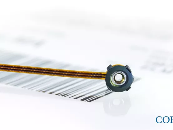
The evolution of industrial and non-industrial automation, smart manufacturing, and Industry 4.0 technologies have increased demand for vision systems that support robust, reliable imaging industrial applications. What factors are driving growth in the machine vision market today?SEMI spoke with Frederic Laune, Business Manager, European Technology, Corning, about how Corning® Varioptic® Lenses are vital to advancing the speed, efficiency, and integration of products using computer imaging. Laune shared his views ahead of his presentation at SEMI MEMS Imaging Sensors Summit, 25-27 September, 2019, at the WTC in Grenoble, France. Join us at the event to meet Corning and many other key industry influencing players. Registration is open.SEMI: Corning's markets include optical communications, mobile consumer electronics, display technology, automotive, and life sciences vessels. Back in June 2019, Corning Incorporated announced that it had delivered its 2 millionth Corning® Varioptic® Lens for industrial applications. What drove this great milestone?Laune: This milestone was met thanks to the fact that Corning Varioptic’s solution solves several problems generated by classical motorized solutions used in industrial applications: limited number of actuation cycles, poor vibration and shock resistance, size (meaning bulky), and high-power consumption. Before Varioptic, there was no variable focus solution that worked well.In addition, the explosion of the CMOS sensor technology helped drive down the cost of imaging solutions for industrial devices, increasing the number of applications and shipping volumes.SEMI: What inspired Corning Varioptic Lenses?Laune: Varioptic was started in 2002 by Dr. Bruno Berge, a French physicist turned entrepreneur. Inspired by the work of Gabriel Lippmann, the 1908 Nobel Prize winner for the invention of color photography, Dr. Berge explored the shape-altering effects of an electric charge when applied to two liquids, a phenomenon referred to as electrowetting. His research ultimately led to the creation of liquid lenses.Fast forward to 2017, when Varioptic became a part of Corning through an acquisition that included Varioptic and Invenios technologies. We believe the synergies from this acquisition will lead to exciting new liquid lens application opportunities that align with Corning’s growth strategy and core capabilities. Corning is one of the world’s leading innovators in materials science. For more than 165 years, Corning has applied its unparalleled expertise in glass science, ceramic science, and optical physics to develop products that transform industries and enhance people’s lives.SEMI: What differentiates traditional camera systems from adjustable lens solutions?Laune: Traditional industrial cameras are usually fixed focus, meaning that the image is sharp only in a limited distance range. Unlike consumer camera applications, there were no good solutions for variable or auto focus cameras in the industrial space. This is due to the intrinsic limitations of motorized technologies.Therefore, customers were using, for example, several cameras to focus at several distances. This compromises the optical quality by closing the objective in order to increase the depth of field, therefore limiting resolution and leading to a need for more light.The cameras using Corning Varioptic’s technology offer more functionality with their ability to focus, whatever the distance, in a fast, reliable, and accurate fashion, and with lower power consumption than traditional mechanical solutions. The upshot is that the product that can withstand heat, vibration, mechanical shocks, and high numbers of focus cycles in tough industrial environments. SEMI: And how is electrowetting enabling industrial devices to capture images and process information quickly and clearly? Laune: In two words: fast and accurate.Electrowetting has unique features – with our two-liquid solution, we combine fast focus with high vibration and shock resistance, and the added benefit of low power consumption.What’s more, our programmable lens can be reconfigured on demand. The lens adapts rapidly and continuously from diverging to converging and can be modeled to support demanding variable focus applications. Our lenses can change their focus in milliseconds, similar to the human eye, and capture fast-moving objects at varying distances. The use of liquid, over mechanical solutions, allows us to create a small form factor, saving precious space and reducing power consumption.SEMI: What industrial applications are taking advantage of this technology? Can you name one example?Laune: 2D barcode readers and industrial vision are our main markets. There is also a strong adoption of our technology in medical applications.SEMI: What does the rise of machine vision mean for manufacturers? Give us one prediction about the opportunities offered by advanced imaging applications.Laune: A great example is the use of 2D barcode readers and liquid lenses to track your ecommerce order, point to point. Another example is full product traceability by implementing a 2D barcode on every component of a given product globally to improve product quality. The varying and adjustable focus abilities of our liquid lens technology make it possible for barcode scanners to track products of different heights, allowing manufactures to improve their processes and logistics.Beyond these examples, tracking and analyzing are booming, thanks to the combination of low-cost CMOS sensor technology, increasing processing power, innovative algorithms (deep learning, AI, neuromorphic processors, etc.), and better image quality due to the progress of lens technology, Varioptic being one.We see an opportunity to improve people’s lives, such as enabling better analysis of medical images and improving the use of cameras in biomedical technologies.SEMI: Quality inspection and automation, adoption of Industrial 4.0 technologies, government initiatives. If you were to choose one, what main factor will drive growth in the machine vision market?Laune: It is difficult to pick just one. I believe that full traceability (monitoring individual parts throughout the production process) has interesting implications as compliance and regulatory efforts ramp up and stronger security of goods becomes more important, particularly as consumers become engaged in food safety and tracing products throughout the supply chain.SEMI: What are your expectations for the SEMI MEMS Imaging Sensors Summit and why would you invite your peers to attend? Laune: I strongly believe in the power of human interactions in technology and science! Ideas come from discussions and physical interactions. The SEMI MEMS Imaging Sensors Summit is a great place to network, meet people, and think about the future! Frederic Laune is the business manager leading the Corning® Varioptic® Lenses business. Laune joined Varioptic as an R D engineer in 2003 after spending the first eight years of his career developing novel active components for the optical telecom industry. At the time, Varioptic was a newly created start-up aiming to develop liquid lens technology for industrial applications. After designing the first two Varioptic commercial products, the Arctic 320 and Artic 416, Laune stepped up as head of Varioptic’s R D department to focus on product and performance improvements. In 2010, he was appointed sales and marketing lead for the company. Varioptic was acquired by Corning Incorporated in early 2017. Laune received a master’s degree in physics and optics from University Pierre and Marie Curie (Paris) in 1995.Serena Brischetto is a marketing and communications manager at SEMI Europe.
Read More