
By Laura Nguyen, SEMI HQ
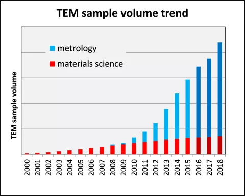
Characterization of materials and devices is critical in determining how an integrated circuit differs from its intended design and function. As advanced designs increasingly require greater process and defect control, demand for Transmission Electron Microscopy (TEM) in semiconductor manufacturing lines is growing significantly.
TEMs are widely used in semiconductor industry for process control, defect analysis and technology development support as the dimensions and details of the features to be investigated are well below the resolution of light microscopes.
The lack of standards impedes the operation of electron microscopes in semiconductor device manufacturing lines as well as the exchange of information and communication between the involved parties.
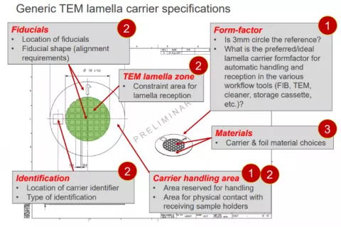
In order to inspect the relevant parts of wafers or devices with TEM, small and thin samples – called lamellas – are prepared from the bulk of the wafer. Lamellas are fragile, however, and must be mechanically supported on carriers and transported manually using tweezers between the different tools during the examination. Standardization of TEM Lamella Carrier (LC) grids will be a big first step in moving beyond manual transport of samples between systems.
Initially, a targeted industry survey was conducted by SEMI to help guide the direction of potential TEM standards activity in spring of 2017. Results were positive, with a majority of the respondents, including major chip manufacturers, confirming the need for standardization and committing to participate in the effort.
The findings of the survey were then presented at SEMICON West 2017 in San Francisco, and the official Electron Microscopy Workflow Task Force was formed under the Physical Interfaces & Carriers North America Technical Committee Chapter. The Task Force was chartered to develop standards needed for workflows involving electron microscopes – scanning electron microscopes (SEM) as well as TEMs – and related equipment in support of development and manufacturing of semiconductor devices as well as silicon and other semiconductor wafers.
The initial task force meeting was held October of 2017. The task force then met monthly to draft the document and gather input from relevant stakeholders across the supply chain, before submitting its initial ballot for voting in February 2019. The first ballot received valuable feedback from the industry that pointed out oversights where several areas of the document could be improved. The task force incorporated this feedback, and the updated document was reballoted in May of 2019. This ballot was approved at SEMICON West 2019, and recently published as SEMI E177-0919, Specification for Transmission Electron Microscope (TEM) Lamella Carriers Used in Electron Microscopy Workflows. This standard is applicable to LCs used for TEM workflows in high volume manufacturing as well as in laboratory environments and covers the form factor and the geometrical dimensions of LCs.
Now that SEMI E177 is published, the task force has begun mapping out the next phase of the electron microscopy workflow to standardize. A recap of the automated TEM workflow was given at the meeting and it was explained that from an automation point of view it is important to have a SEMI Standard not only for the LC, but also for a LC Container.
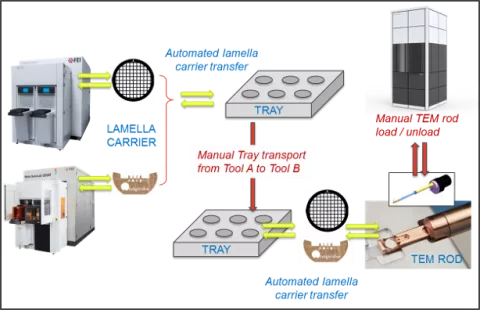
A standardized LC Container would be another big step towards automation workflow, allowing LCs to be transported between different types of TEM workflow tools from different suppliers.
The next task force meeting will be held via teleconference on September 19, 2019 at 15:00 Pacific Time. Please contact Laura Nguyen at [email protected] to be added to the meeting invite.
The next face-to-face task force meeting is scheduled for November 5, 2019 in conjunction with the SEMI Standards North America Fall Meetings at SEMI Headquarters in Milpitas, California. To attend these meetings, you must be a SEMI Standards Program member. There is no cost, but registration is required.
Get Involved
SEMI Standards development activities take place throughout the year in all major manufacturing regions. To get involved, join the SEMI International Standards Program at: www.semi.org/standardsmembership.
For more information please visit our main Web site and current events page. If you have any questions regarding SEMI Standards activities, please contact your local SEMI Standards staff.
Standards Watch
SEMI
www.semi.org
September 12, 2019