
Analyzing Carrier Profile by Scanning Capacitance Microscopy (SCM) and Scanning Spreading Resistance Microscopy (SSRM)
By Kevin Nguyen, SEMI HQ
Silicon, a semiconductor, is used in device fabrication. Silicon by itself is a nonconductive material, but when doped with boron or phosphorus, it generates electrically charged carriers and conducts electron flow. Semiconductors are used to create trillion of transistors in today’s integrated circuit chips.
Physical characterization at the microscopy level of semiconductor devices have always been a challenging task for device engineers, process engineers and researchers. A tiny defect can lead to device failure. It is imperative that an accurate carrier profile data to be provided, so electrical properties can be characterized to support and drive the limit of technology.
As technology nodes shrink further towards 7nm, device fabrication is becoming increasingly challenging. Intel, TSMC, and Samsung are the only three manufacturers that are working on a 7nm process today.
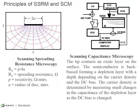
Smaller device geometry and higher reliability requirements will need new characterization tools. Present practices of Scanning Capacitance (SCM) and Scanning Spreading Resistance Microscopy (SSRM) (refer to image below) are widely used in carrier profiling techniques employed in the analysis of semiconductor devices, but no industry consensus standard that captures optimal practices exists.
To address this vacuum, at the Silicon Wafer NA TC Chapter meeting, July 9, 2019, in San Francisco, CA, during SEMICON West, the committee authorized the Int’l Test Methods Task Force to start drafting
This effort is led by Umberto Celano (IMEC) and Mark Hagmann (NewPath Research). Initial Working Group (WG) members represent industry stakeholders such as GlobalFoundries, Druker, IMEC, Micron, NIST, Rudolph Technologies, and NewPath Research.
The WG will be addressing test repeatability and resolution where the measurements are made at multiple locations on a sample. The goal is to come up with a standard for definition, concentration precision, dynamic range, vertical steepness, and other requirements for carrier profiling. Development of an industry-consensus Standard will enable manufacturers to effectively conduct root-cause failure analysis and improve production yield.
The task force anticipates having a draft available for discussion at the March 31, 2020 meeting in conjunction with NA Standards Spring meetings in Milpitas, California. The ballot will then be issued in May for technical adjudication and approval in July 20-21, 2020 meeting in San Francisco, CA at SEMICON West.
If you would like to join the task force, please contact Kevin Nguyen at [email protected]
Get Involved
SEMI Standards development activities take place throughout the year in all major manufacturing regions. To get involved, join the SEMI International Standards Program at: www.semi.org/standardsmembership.
For more information please visit our main Web site and current events page. If you have any questions regarding SEMI Standards activities, please contact your local SEMI Standards staff.
Standards Watch
SEMI
www.semi.org
September 12, 2019