
Improved High Precision Dopant/Carrier Concentration Profiling with Corona-charge Non-contact C-V (CnCV)
Academic Paper Provided By Semilab Inc.
Abstract
We report significant advancements in corona-based non-contact capacitance-voltage (CnCV) metrology recently developed for comprehensive C-V characterization of SiC and other wide bandgap semiconductors. The technique answers the industries needs for nondestructive, costeffective C-V dopant monitoring for material and device development and manufacturing control. Excellent precision and matching to mercury probe CV is demonstrated for SiC, Ga2O3, GaN and AlGaN/GaN structures over a concentration range from 1014cm-3 to 2x1019cm-3 . The emphasis in the present work is on improvement of CnCV in dopant depth profiling resolution and measurement throughout. This is achieved with a variable charge method that in-situ adjusts corona charging increments in response to changes in dopant concentration. Results are presented for multi-layer epitaxial SiC and for 2DEG in AlGaN/GaN HEMT structures. The latter represents an extreme case of high-low concentration profiling with a transition from 1020 electrons/cm3 in the 2D electron gas to a fully depleted well and dopant concentration in the 1015cm-3 range.
Introduction
Capacitance-voltage, C-V, is a leading technique for characterization of dopant concentration in semiconductors materials and devices. Conventional C-V involves fabrication of electrical test structures. This increases the cost of characterization and results in slow data feedback that can take weeks. Temporary contact mercury probe Hg C-V offers a solution [1], however it creates the danger of Hg contamination. The CnCV technique that is based on the corona-Kelvin method provides a non- destructive preparation-free alternative. Since the 1990’s, corona-Kelvin has been widely adopted in silicon fabs, primarily for dielectric and interface characterization [2,3]. Successful extensions to wide bandgap semiconductors have led to the development of commercial non-contact electrical metrology tools that have already proven very effective in a broad range of applications including precise dopant concentration measurement and characterization of interfaces and dielectric films as discussed in ref. [4] and in a 2017 review [5] followed by commercial introduction of a new line to CnCV tools. The goal of the present work is further improvement of the CnCV technique in dopant characterization and depth profiling.
Experimental
The measurement principles of the corona-Kelvin technique are described in ref. [2] and [3], while the details specific to the measurement of wide bandgap semiconductors are given in ref. [5]. The key for understanding the corona-charge biasing principle is the surface-bulk electrical neutrality and mirroring of the corona deposited charge in the semiconductor space charge region. The corona charge-based metrology uses sequential charging increments, DQC, with a polarity determined by the corona source voltage. Corresponding sequential, non-contact measurements of surface voltage, V, are performed with a Kelvin probe. The corona-Kelvin apparatus is shown schematically in Fig. 1. During the measurement, the semiconductor wafer is held on a conducting chuck by vacuum suction. The moveable chuck cycles the wafer test site between the corona charging source, on the left in Fig. 1, and position under the vibrating Kelvin probe, on the right in Fig. 1. For dopant concentration measurement, negative charging is used for n-type material and positive charging is used for p-type material. This corona charge biasing moves the surface deeper into depletion with each consecutive charging step. Each charge increment (DQC) and corresponding change of the surface voltage (DV) gives the non-contact capacitance, C=DQC/DV, that corresponds to voltage V and to the cumulative deposited charge, Q=SDQC. The set of sequential measurements give the C-V, C-Q, and V-Q characteristics. CnCV is a quasi-static technique providing low frequency capacitance characteristics. The magnitude of the charge increment is the quantity that determines the probing depth resolution given by a change of the depletion width (DW) in each increment. For a dopant concentration, ND, the probing depth increment is DW=DQC/qND. The value of DQC is precisely controlled using a potential compensator and in-situ charge monitoring as shown in Fig. 1. During corona charging the potential compensator adjusts the wafer potential to the same precharging value. The in-situ charge monitoring determines DQC in each charging step.
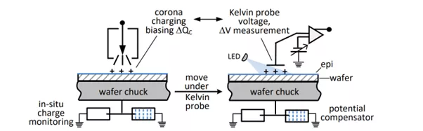
Fig. 1. Schematic of the corona-Kelvin measurement apparatus used in the CnCV technique
The ions created by the corona discharge are thermalized while diffusing in air and are deposited on the semiconductor surface having negligible kinetic energy. This results in a completely non invasive measurement. However, low energy ions can be easily repelled or attracted by previously deposited charge. This electrostatic interaction would alter the charge dose and the surface charge distribution in the charging sequence, leading to uncertainty in the DQC value. The new generation of corona charging eliminates such electrostatic effects by compensation of the surface potential to exactly the same value prior to each charging increment [6]. This new feature is combined with insitu charge monitoring and assures very high precision of DQC over the practical range from 1010 to 1012 q/cm2 used in CnCV tools for the dopant measurement. The lowest DQC is used for low dopant concentration in the 1014cm-3 range, while high DQC is required in the high concentration measurement range of 1019cm-3 . Traditionally, in a corona charge bias sweep, DQC was adjusted to a constant value suitable for a low ND region. As a result, the scanning through a high concentration region required a large number of increments that diminished the measurement throughput.
The improved corona-charge metrology introduces “smart charge biasing” with a variable DQC. Specifically, the method adjusts DQC to higher values for regions with higher dopant concentration and to lower DQC values for regions with low dopant concentration. The dose changing point in the charge bias sweep is determined with an algorithm based on the change of derivative of the surface voltage.
Additional difficulty in implementation of this apparently simple idea was related to the need for absolute calibration of the variable DQC with a very high precision. Such a reliable procedure was developed and tested, confirming equivalency of measurement with a variable DQC to within 0.05%.
The LED illumination under the Kelvin-probe indicated on the right side in Fig. 1 is used for determination of the flatband condition in passivated wafers with dielectrics. It is not used in dopant measurement on bare wafers.
Results and Discussion
Basic CnCV dopant measurement. The corona charge bias sweep in the CnCV technique gives the capacitance, C, and the surface voltage, V, as a function of the charge density, QC. All three characteristics; C vs. QC, V vs. QC and C vs. V are used in CnCV metrology. However, by analogy to conventional C-V, CnCV uses non-contact C-V and the inverse derivative value [d(1/C2 ) /dV] -1 for dopant measurement. Since the commercial introduction of the technique, we have performed numerous demo measurements on wide bandgap semiconductors and structures, SiC, GaN, AlGaN/ GaN and most recently on epitaxial Ga2O3. Continuous refinement enabled the extension of measurements in the high doping and in low doping range. The experimental results illustrating such measurements are given in Fig. 2 and in Fig. 3 for p+ epitaxial GaN doped with Mg and for low level nitrogen doped n-type epitaxial SiC, respectively. The measurements were performed with high corona charging increments (DQC of 1x10¹² q/cm2 ) and low increments (2x10¹⁰ q/cm2 ), respectively. The corresponding depth increments, DW, were 0.5nm and 700nm. A large difference in voltage range is seen for two dopant concentrations. It should be noted that precise measurement of low dopant uses high surface voltages of up to 80V. Such measurements require a new generation of corona charging that incorporates a surface voltage compensation method.
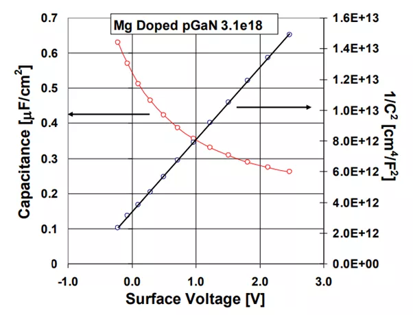
Fig. 2. C-V and 1/C2 -V plots for high Mg doped p-type epitaxial GaN.
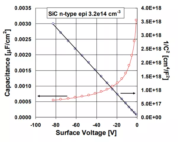
Fig. 3. C-V and 1/C2-V plots for low N-doped, n-type epitaxial 4H-SiC.
In Fig. 4 we show the currently updated correlation plot between CnCV dopant and Hg-CV or nominal dopant concentration. The plot includes p-type and n-type results for different wide bandgap semiconductors and structures. Compared to previous versions, this plot incorporates new results for Ga2O3, highly doped p +GaN and 2DEG electron concentration in HEMT that approaches 1020cm-3 .
Variable charge dose measurement of epitaxial SiC. The actual application of the improved doping depth profiling is illustrated in Fig. 5 by measurement results on n-type SiC with two epitaxial layers of different dopant concentration on highly doped substrate.
The profiling was performed using negative corona charging with increasing doses. The inverse derivative of 1/C2 was used for dopant calculation at the depth determined by the value of capacitance. For the low dopant concentration of 6x1014cm-3 in the top layer a dose of 3x10¹⁰q/cm2 was used, increasing the depletion width by about 0.5µm per charging increment. After reaching about 7µm, the transition to a higher doping was detected and the dose was increased to 2x10¹¹q/cm2 . With the increased dose, the profiling of the layer with 9x1015cm-3 dopant concentration proceeded with depth increments of about 0.2µm.
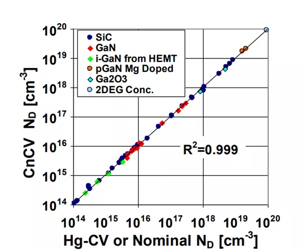
Fig. 4. Correlation plot between CnCV dopant and Hg-CV or nominal dopant concentration.
At a depth of about 9µm the next transition to the higher doped substrate was detected and the corona dose was increased to 1x10¹²q/cm2 . The expanded depth profile in the transition region and the substrate is shown on the right in Fig. 5. It is seen in Fig. 5 that using variable charge dose the entire profiling was completed with using about 50 charge-measure increments taking total time of 3 minutes. With constant dose charging adjusted to the lowest dopant concentration the profiling would take about 30 minutes. The gain of throughput is evident.
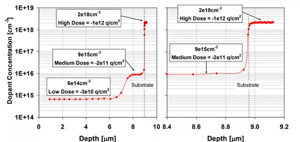
Fig. 5. Dopant depth profile of multilayer epitaxial n-type SiC measured with a variable dose method. The profile on the right shows an expanded transition region from the medium doped layer to the highly doped substrate.
Variable dose measurement of 2DEG in HEMT. An important application of the improved metrology is illustrated in Fig. 6, 7, and 8 with results for a GaN/AlGaN/GaN HEMT structure. In this case, two charge increments were used. A high dose of 3x10¹¹ q/cm2 was used in the high electron concentration range with a populated 2DEG. A low dose of 3x10¹⁰ q/cm2 was used in profiling while the 2DEG was depleted. Three different characteristics were all obtained in one measurement with positive corona sweep after negative corona pre-charging. Figure 6 presents the C-Q characteristic. The corona charge on the x-axis is the net charge with zero corresponding to the initial condition. The charge to depletion and the charge at the pinch-off point are unique parameters in characterization of the HEMT structure. They are readily available in the coronacharge method. Corresponding voltage values are shown in the C-V characteristic in Fig. 7. The carrier concentration profile in Fig. 8 is calculated from the C-V using the derivative procedure adopted from ref. [7]. The high dose range covers 20 charge-measure increments giving adequate information on the 2DEG concentration and depth. Without the variable charge method, 200 small corona charge increments would be used resulting in large noise in the derivative determination of carrier concentration and a much longer measurement time: 30 min. vs. 4 min. with the new method. The actual throughput improvement in this case was about 8 times which is quite important for practical CnCV applications.
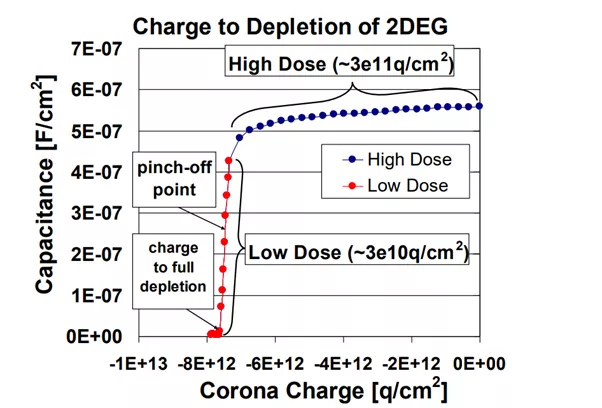
Fig. 6. C-Q characteristic on GaN/AlGaN/GaN HEMT structure illustrating use of the smart charge biasing method with variable corona charge.
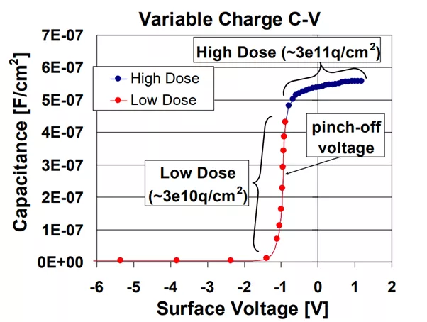
Fig. 7. C-V characteristic on GaN/AlGaN/GaN HEMT structure illustrating use of the smart charge biasing method with variable corona charge.
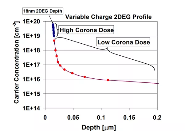
Fig. 8. 2DEG carrier concentration profile of GaN/AlGaN/GaN HEMT structure illustrating use of the smart charge biasing method with variable corona charge.
Conclusion
The present results demonstrate recent progress in dopant concentration and electron concentration measurement with the non-contact CnCV metrology including an expanded range and depth profiling with an 8 times improvement in throughput.
The later was realized with in-situ variable corona-charging dose. We believe that the present improvements shall benefit cost effective development and fabrication of wide bandgap semiconductor devices.
Get Involved
SEMI Standards development activities take place throughout the year in all major manufacturing regions. To get involved, join the SEMI International Standards Program at: www.semi.org/standardsmembership.
For more information, please visit our main Web site and current events page. If you have any questions regarding SEMI Standards activities, please contact your local SEMI Standards staff.
References
[1] D. Schroder, Semiconductor Material and Device Characterization, 3rd ed. (John Wiley and Sons, Inc., Hoboken, New Jersey, 2006), pp.61-78.
[2] Ibid, pp.523-562.
[3] M. Wilson, D. Marinskiy, A. Byelyayev, J. D’Amico, A. Findlay, L. Jastrzebski and J. Lagowski, ECS Transactions, 3 (3), p. 3-24 (2006).
[4] A. Savtchouk, M. Wilson, J. Lagowski, Materials Science Forum, 897 (2017) 139-142.
[5] M. Wilson, A. Findlay, A. Savtchouk, J. D'Amico, R. Hillard, F. Horikiri and J. Lagowski, ECS J. Solid State Sci. Technol. 6-11 (2017) S3129-S3140.
[6] A. Savtchouk, M. Wilson, J. Lagowski, A. Czett, and C. Buday, Materials Science Forum, 858 (2016) 509-512.
[7] O. Ambacher et. al, J. Appl. Phys., 85-6 (1999) 3222-3231.
Standards Watch
SEMI
www.semi.org
September 12, 2024