Mercury Free Test Method for Characterizing Silicon Wafer is Underway
By Kevin Nguyen, SEMI HQ
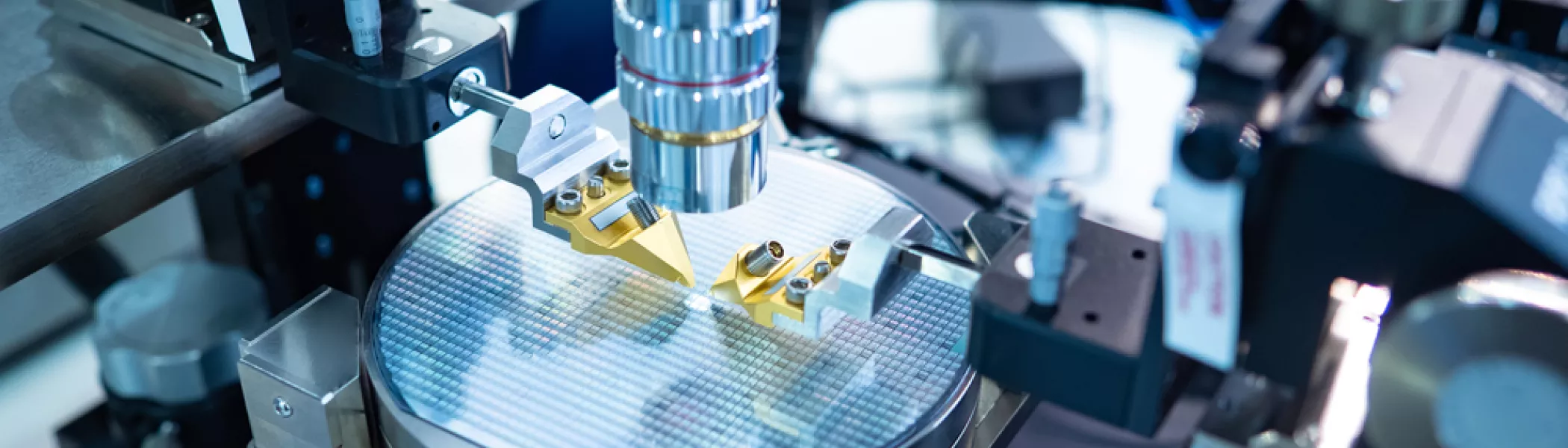
SEMI MF1392 -Test Method for Determining Net Carrier Density Profiles in Silicon Wafers by Capacitance-Voltage Measurements with a Mercury Probe is the industry choice for characterizing epitaxial layer of silicon wafers. This standard specifies the method for determining net carrier density profiles in silicon wafers using capacitance-voltage (CV) measurements with a mercury probe. By utilizing this technique, manufacturers can accurately assess the carrier density and resistivity of epitaxial silicon wafers, which are crucial parameters for optimizing semiconductor device performance and quality performance.
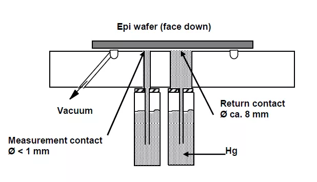
HgCV Principle Based on a Schottky Diode
However, mercury (Hg) is a poisonous and environmentally harmful element. The Minamata Convention, named after Minamata, Japan, the city that went through a devastating mercury poisoning incident in 1953 with thousands of casualties, includes bans on the use of mercury. This international treaty is designed to protect human health and the environment from the adverse effects of mercury. Enforced since August 16, 2017, it aims to minimize the release of mercury into the environment and control its use in various products and processes.
To protect human health and the environment, it is extremely essential to develop and standardize alternative methods to HgCV. Alternative methods are available in the market but there are no standards in the semiconductor industry.
At SEMICON Europa on November 16, 2023, the Silicon Wafer EU Technical Committee Chapter authorized Document 7162, New Standard: Test Method for epi-resistivity determination in Si wafers by Surface Charge Profiling, which was submitted by the International Test Methods Task Force, led by Armin Kempf (Siltronic).
GlobalWafers, Semilab, SEH, SUMCO, and Siltronic are coming together to address the challenges posed by the Minamata Convention and to work collaboratively towards finding safer alternatives for semiconductor characterization processes. Despite an aggressive schedule, the task force’s goal is to complete this standard by the end of 2024.
If you would like to participate in this task force, please contact Kevin Nguyen at [email protected].
Get Involved
SEMI Standards development activities take place throughout the year in all major manufacturing regions. To get involved, join the SEMI International Standards Program at: www.semi.org/standardsmembership.
For more information, please visit our main Web site and current events page. If you have any questions regarding SEMI Standards activities, please contact your local SEMI Standards staff.
Standards Watch
SEMI
www.semi.org
June 13, 2024