
Newly Formed Silicon Carbide Epitaxial Defects and Engineered Substrate Task Forces
By Kevin Nguyen, SEMI HQ
Epitaxial layers of silicon carbide (SiC) play a pivotal role in the design of power electronic devices, offering enhanced performance, efficiency, and reliability compared to traditional semiconductor materials such as silicon.
In-depth analytical techniques are instrumental in gaining a comprehensive understanding of SiC epitaxial layers, enabling manufacturers to optimize the fabrication process and produce high-quality SiC-based devices for power electronics applications. Despite reports on defects in these epitaxial layers and associated measurement techniques, there exists ambiguity in the nomenclature of these defects. Establishing consistent and standardized terminologies are crucial in the compound semiconductor materials industry, particularly in the context of reporting and comparing results related to epitaxial layers and defects.
The SiC Epi Defects Task Force (TF), led by Christian Kranert (Fraunhoffer), was formed during the SEMICON Europa 2023 standards meetings with the objective of standardizing common terminology and defining measurement techniques for silicon carbide epitaxial layers. This initiative, in accompany with SEMI M81, Guide to Defects Found in Monocrystalline Silicon Carbide Substrates, involves a systematic and collaborative approach.
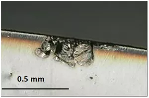
Edge Chip and Indent (source: SEMI M81)
The TF was charted to develop SEMI Draft Document 7160, a new Standard titled “Guide for Defects Found in Homoepitaxial Layers of Silicon Carbide”. Key industry players, including Bosch, Fraunhofer, GlobalWafers, Infineon, KLA, SiCrystal, SOITEC, Wolfspeed, XFAB, have actively joined this effort.
Additionally, the Compound Semiconductor Materials Europe Technical Committee Chapter also approved a new task force for Silicon Carbide Engineered Substrate, aligning seamlessly with the increasing demands for electrification. Enrica Cela of SOITEC will spearhead this activity. Given SiC’s renowned properties, engineered substrates have the potential to further elevate performance.
The engineered substrate, comprising direct-bonded substrates of silicon carbide with diameters of 150 or 200 mm, is integral to this effort. Establishing precise properties for the electrical, structural, and dimensional characteristics of polycrystalline and monocrystalline layers within the context of silicon carbide (SiC) substrates is critical for ensuring the reliability and performance of semiconductor devices.
This new initiative will build upon fundamental principles, including dislocations and bulk defects from SEMI M55, Specification for Polished Monocrystalline Silicon Carbide Wafers. Key industry players such as SOITEC, ST Microelectronics, SiCrystal, and Wolfspeed have enthusiastically joined this growing TF, underscoring the significance of this collaborative endeavor.
If you would like to participate in either of these activities, please contact Kevin Nguyen at [email protected].
Get Involved
SEMI Standards development activities take place throughout the year in all major manufacturing regions. To get involved, join the SEMI International Standards Program at: www.semi.org/standardsmembership.
For more information, please visit our main Web site and current events page. If you have any questions regarding SEMI Standards activities, please contact your local SEMI Standards staff.
Standards Watch
SEMI
www.semi.org
December 18, 2023