
300 mm Tape Frame FOUP Related Standards Published
By Hayato Iwamoto, SEMI Japan Region PI&C (Physical Interfaces & Carriers) Technical Committee, 300 mm Tape Frame PI&C Task Force Co-Leader, Sony Semiconductor Solutions Corporation
After three years of standardization activities, the 300 mm Tape Frame FOUP Standards SEMI E184 and SEMI E185 was published in December 2021.
- SEMI E184, Specification for 300 mm Tape Frame FOUP Load Port
- SEMI E185, Specification for 300 mm Tape Frame FOUP
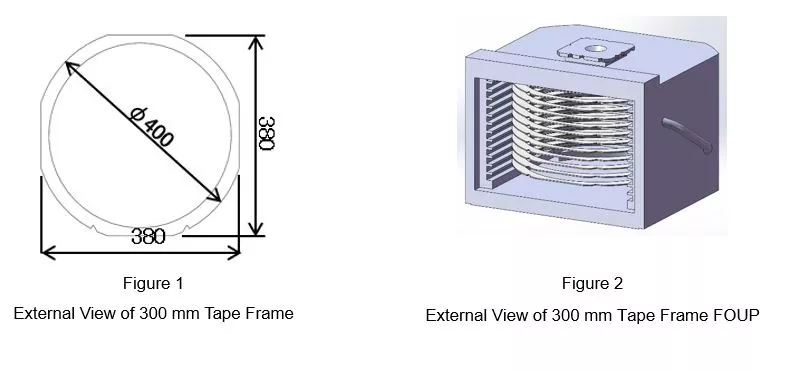
Conventionally, metal-based open cassettes have been used in semiconductor back-end processing lines. However, in response to the increasing demand for quality, it has been necessary to secure a sealed space similar to that used in the front-end process in order to reduce particles that greatly affect the characteristics of silicon devices. In July 2018, the 300 mm Tape Frame PI&C Task Force was established under the umbrella of the Physical Interfaces & Carriers (PI&C) Technical Committee in Japan. The task force recognized the need for a 300 mm FOUP standard, which is widely used in the front-end process, due to its insufficient diameter size. At the committee meeting in April 2021, the ballot (electronic voting) of the document was discussed and passed, and later published in December 2021.
The 300 mm Tape Frame PI&C Task Force was led by Sony Semiconductor Solutions Corporation and Tokyo Seimitsu Co., Ltd., and was attended by more than 60 members from 30 companies, including device manufacturers, foundries, and OSATs from the United States and Taiwan. Active discussions took place regarding the dimensions of FOUP containers, the number of containers to be accommodated, and the spacing between slots.
The newly published SEMI E184 and SEMI E185 are sealed containers based on the same concept as the 300 mm standard FOUP (SEMI E47.1). By adopting these containers, it is possible to realize highly clean transportation between processes required for post-process leading processes. As a result, it is expected that device manufacturers and OSATs, which have post-process processes using tape frames, will contribute to maintaining and improving the quality of manufactured devices.
SEMI Standards forms the foundation of innovation in the microelectronics industry. The SEMI Standards development process is based on the activities of over 5,000 volunteers and is used to develop over 1,050 industry-recognized standards and guidelines.
If you would like to participate in the standardization activities of the SEMI Standards Japan Physical Interfaces & Carriers (PI & C) Technical Committee, please contact: Mami Nakajo, SEMI Japan Standards & EHS Department at [email protected].
Get Involved
SEMI Standards development activities take place throughout the year in all major manufacturing regions. To get involved, join the SEMI International Standards Program at: www.semi.org/standardsmembership.
For more information, please visit our main Web site and current events page. If you have any questions regarding SEMI Standards activities, please contact your local SEMI Standards staff.
Standards Watch
SEMI
www.semi.org
March 7, 2022