
Introducing New MEMS Standards
By Alissa Fitzgerald, A.M. Fitzgerald & Associates
The next time you find yourself in your neighborhood hardware store, take a stroll down the aisle containing fasteners. Behold the rows and rows of drawers containing fasteners of all sizes, identified with labels such as #10-32 or M6. In almost every city on the planet, you may find these same fasteners. Have you ever thought about how this came to be?
The answer, of course, is standards. Standards come about when practitioners recognize that the value of sharing information is greater than the value of hoarding it. The need to repair steam locomotives wherever they broke down motivated 19th century mechanical engineers to create standardized screw threads, so that replacement fasteners could be quickly and locally acquired. Prior to that standard, fasteners were not interchangeable, because every machine shop made its own proprietary screw thread. [1]
A joint workshop at Semicon West 2015, “Creating solutions to address common challenges facing the MEMS, Sensor and Semiconductor Industries in the next decade," organized SEMI and the then MEMS Industry Group (MIG), launched the beginning of an earnest effort to develop standards useful for MEMS.
There had been much talk for years at MIG events about finding a way to bring standards to the MEMS industry, to tame its proliferation of custom process flows and substrates. A widely-held opinion was that the diversity of MEMS devices made developing standards too difficult; yet at the same time, most agreed that standards would be needed to overcome business inefficiencies and to help the MEMS industry live up to its full commercial potential. The challenge was figuring out where to begin. With so many MEMS companies spending tens of millions of dollars to bring their proprietary devices to market, there seemed to be more motivation to hoard hard-won knowledge than to share it.
In her keynote talk at the 2015 workshop, Alissa Fitzgerald proposed two topics for attendees to consider. Influenced by her early career experience working with standardized fasteners and cutting tools in the aerospace industry, she suggested two MEMS analogues, SOI wafers and deep reactive ion etch (DRIE), as topics for new MEMS standards. Specifying these two frequently customized and costly items in MEMS fabrication were pre-competitive challenges experienced broadly across both the MEMS and semiconductor industries and therefore ripe for collaboration on standards.
Following the 2015 workshop, a Working Group began to meet monthly to begin the work of exploring and defining new MEMS standards. To launch the formal Standards development effort with SEMI, Chris Moore, Covalent Metrology, assembled the first SEMI Standards New Activity Report Form (SNARF) on SOI wafers for MEMS, and Rich Allen, NIST, drafted a SNARF for DRIE. Both contributed their long experience working on multiple SEMI Standards documents to help guide their MEMS colleagues who had never done so.
Over the next few years, more than two dozen MEMS industry colleagues, hailing from government laboratories and materials, EDA, foundry, equipment and design companies, met monthly to discuss and refine the technical content. During at least two Semicon West events, the committee huddled in a windowless room to pore over every word, definition, reference and diagram in the evolving documents. It was truly a group effort to pool the expertise of so many people, practicing in different areas of the industry, in order to create clear and helpful content for the document’s future readers.
Key technical inputs to both standards were provided by Rich Allen, NIST; Michelle Bourke, Lam Research; Alissa Fitzgerald, A.M. Fitzgerald & Associates; Mary Ann Maher, SoftMEMS; Petri Santala, Okmetic; Steve Martell, Sonoscan; Chris Moore, Covalent Metrology; Dave Mount, ULVAC; Magnus Rimskog and Carlos Stahr, Silex Microsystems.
In 2017, MIG merged with SEMI and became the MEMS & Sensors Industry Group (SEMI-MSIG), a change which benefited the committee’s efforts by adding SEMI’s significant resources. Carmelo Sansone coordinated SEMI’s resources and Laura Nguyen, SEMI’s senior coordinator of international standards, with help from Soomin Chung, added knowledge of the SEMI standards database and long experience with writing and balloting standards. Michelle Bourke, Lam Research, took over leadership of the committee in 2018 with new energy to move the standards onto balloting. Tim Brosnihan, Executive Director of SEMI-MSIG, gave the DRIE standard a final push forward by providing several illustrations and mask layouts.
The SOI standard, SEMI MS12-0220 - Specification for Silicon Substrates Used in Fabrication of MEMS Devices, provides key definitions and details for specifying the mechanical and electrical features of SOI substrates for use in MEMS manufacturing. It became the first MEMS-specific wafer standard, released in 2020. With time, the committee hopes that this standard will assist material suppliers to stock common SOI wafer configurations, improve availability and reduce cost, and assist buyers to more clearly and accurately communicate specifications for custom SOI wafers.
The DRIE standard, SEMI MS13-0221 - Guide for Use of Test Patterns for Characterizing a DRIE Process, defines a variety of lithographic test patterns that are useful for characterizing and tuning a DRIE process. In DRIE, etch performance is highly sensitive to recipe parameters, masking preparation and pattern geometry, and requires iterative tuning to maximize device yield. The standard is applicable for DRIE of both MEMS and semiconductor devices. The committee hopes that it will reduce the time spent by process engineers on tuning DRIE performance for a particular device pattern and help them to better monitor etch quality and equipment performance over time. The standard was published in February 2021.
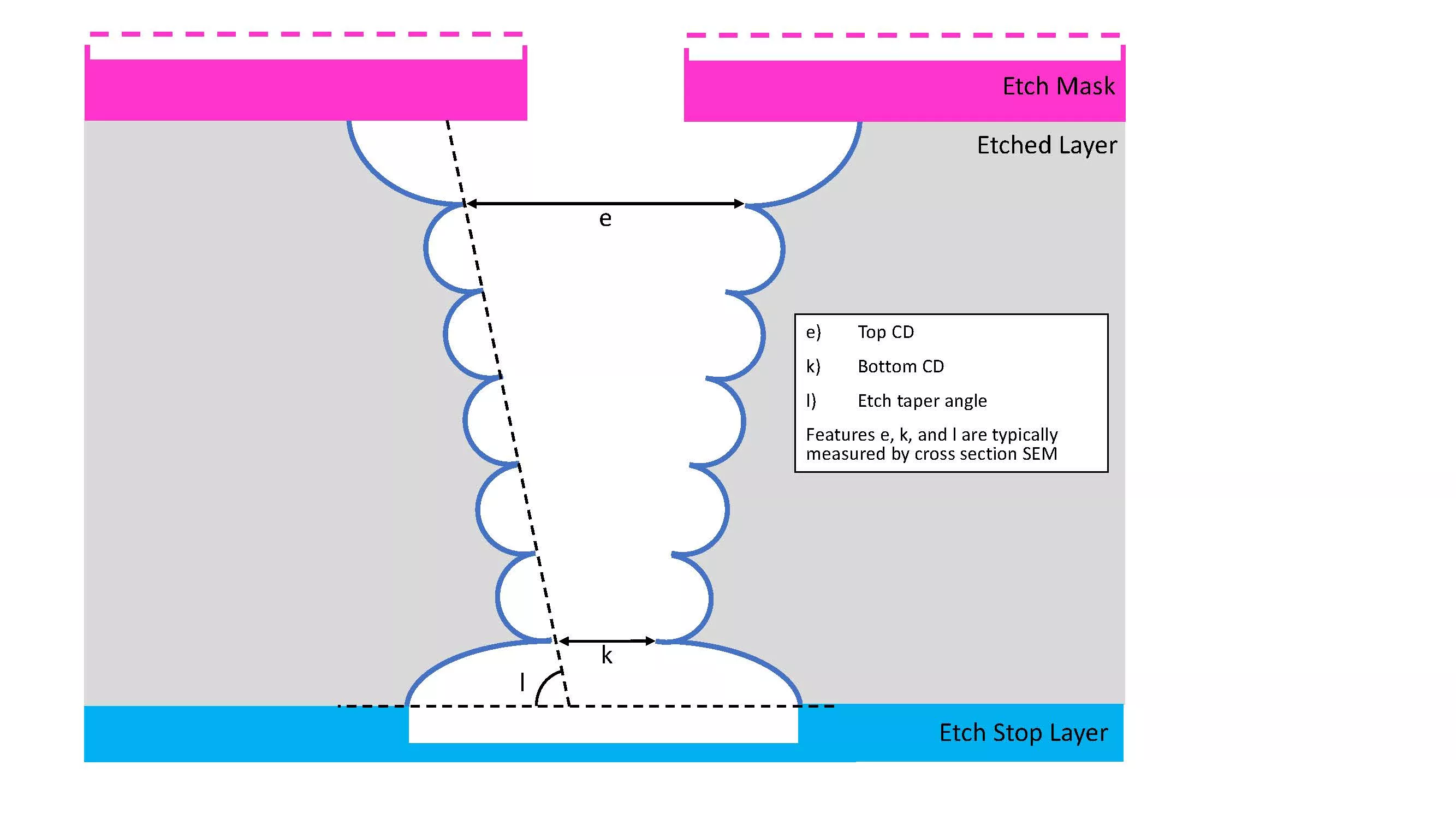
The figure below shows a tapered etch profile where the feature’s top critical dimension is larger than the bottom critical dimension [SEMI MS13, Figure 5].
In the meantime, the MEMS Working Group continues to identify and develop more MEMS-specific standards. If you have ever wondered, “well, why isn’t there a standard for x?”, it’s because you haven’t yet joined our committee to help write it. New members are welcome at any time!
Get Involved
SEMI Standards development activities take place throughout the year in all major manufacturing regions. To get involved, join the SEMI International Standards Program at: www.semi.org/standardsmembership.
For more information, please visit our main Web site and current events page. If you have any questions regarding SEMI Standards activities, please contact your local SEMI Standards staff.
References
1. https://www.asme.org/about-asme/engineering-history/landmarks/234-the-united-states-standard-screw-threads
Standards Watch
SEMI
www.semi.org
March 11, 2021