200mm Silicon Carbide Wafer Specification and Marking - An Update
By Kevin Nguyen, SEMI
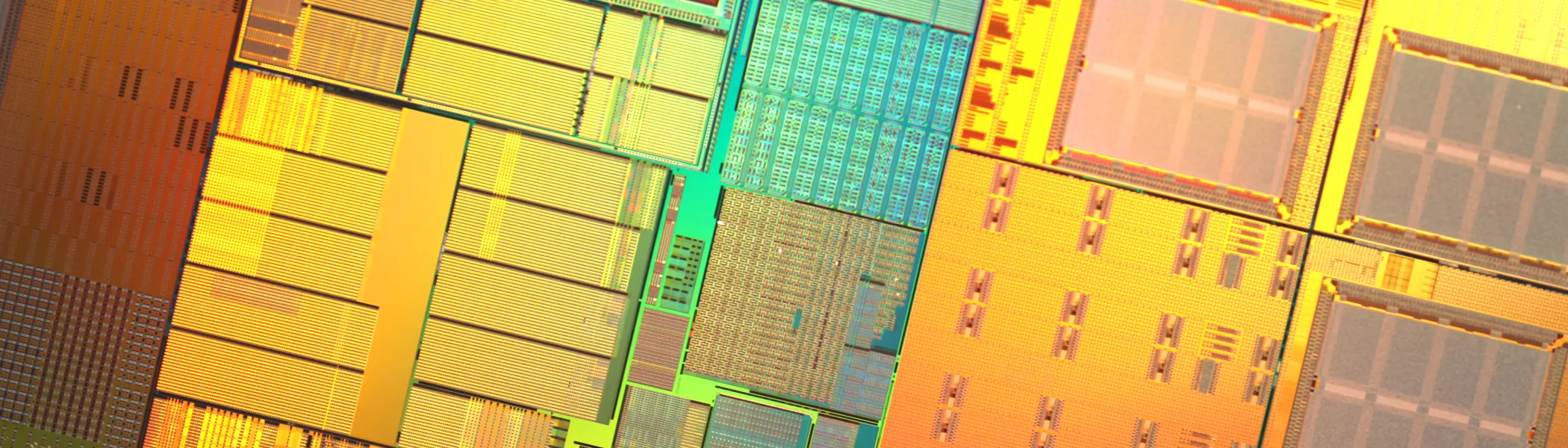
SEMI M55, Specification for Polished Monocrystalline Silicon Carbide Wafers, initially developed in 2004 for 50mm wafers, has been updated over the years to add specifications for 76.2mm, 100mm, and 150mm wafers. This latest proposal seeks to establish requirements for the 200mm generation.
Since last summer, Applied Materials and GlobalFoundries have joined the SiC Material and Wafer Specification Task Force (TF), which has been meeting monthly via Web conference every last Thursday of the month from 7:00-8:00 AM Eastern Time.
Both silicon carbide users and suppliers have stakes in this proposal. To address all concerns, the TF has mapped out a timeline and allocates time in each meeting to discuss each section thoroughly.
This strategy seems to be paying off. Significant progress has been made on defining electrical properties and physical characteristics (e.g., thickness and tolerance, edge shape, flatness, orientation, and defects). The remaining sections, including test methods and certification, were the main focus of the December 2020 meeting, and the TF was able to finalize Document 6615: Revision to SEMI M55, Specification for Polished Monocrystalline Silicon Carbide Wafers. The document is currently available for voting in Cycle 2-2021. The results will be discussed in April 2021 at the Compound Semiconductor Materials Europe TC Chapter meeting.
Correspondingly, Tom Barbieri (Wolfspeed/Cree) has also proposed Document 6604: Revision to SEMI T5-1214, Specification for Alphanumeric Marking of Round Compound Semiconductor Wafers, to include marking for 200mm silicon carbide. The current version of SEMI T5 covers 200mm compound semiconductor wafers, however, it does not specifically address marking for silicon carbide. The TF has incorporated feedback from its initial ballot attempt, and plans on issuing Ballot 6604A in March 2021.
Get Involved
SEMI Standards development activities take place throughout the year in all major manufacturing regions. To get involved, join the SEMI International Standards Program at: www.semi.org/standardsmembership.
For more information, please visit our main Web site and current events page. If you have any questions regarding SEMI Standards activities, please contact yourlocal SEMI Standards staff.
Standards Watch
SEMI
www.semi.org
March 11, 2021