
Japan Panel Level Packaging Panel FOUP Activity Highlights
By Shoji Komatsu, Acteon NEXT
The activity of the Panel Level Packaging (PLP) Panel FOUP Task Force (TF) started in May 2018 and over 40 Task Force meetings have been held since its foundation. Over 40 participating companies and 95 registered TF Members contribute to this effort.
The Panel FOUP Standards suite was recently published this past March for the two panel sizes of 510 mm × 515 mm and 600 mm × 600 mm standardized in the SEMI 3D20: Specification for Panel Characteristics for Panel Level Packaging (PLP) Applications.
Task Force Activity Policy
In order to realize smooth implementation of PLP, standardization of physical interfaces such as FOUP and LP is considered to be prerequisite by the relevant suppliers from cost performance and time-to-market point of views. After several discussions, the Panel Level Packaging (PLP) Panel FOUP TF currently assumes two sizes of panels, 510 mm × 515 mm sizes and 600 mm × 600 mm sizes based on the SEMI 3D20 Standard.
Standard Structure
The Panel FOUP standard consists of one parent document and four subordinate documents.
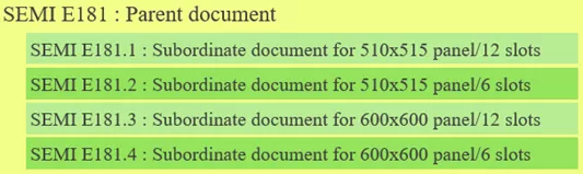
Figure 1 Standard Structure
The user can select 6 slots or 12 slots based on the panel characteristics and panel / carrier weight.
Overview of panel FOUP
Figure 2 shows the Door Features. The left side of the figure shows the 600 mm × 600 mm panel, and the right side of the figure shows the 515 mm × 510 mm panel. You can see that the positions of the latch key and the door suction pad are the same, but only the width is different.
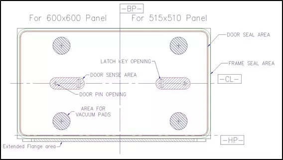
Figure 2 Door Features
Figure 3 shows the bottom Features. The left side of the figure shows the 600 mm × 600 mm panel, and the right side of the figure shows the 510 mm × 515 mm panel. The kinematic coupling, hold-down, sensing pad position, etc. are the same for each panel size, but only the conveyor rails used for transfer such as PGV and AGV are positioned and sized according to each panel size.
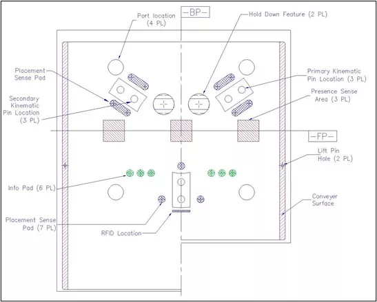
Figure 3 Bottom Features
Figure 4 shows the Panel Support Area. Unlike silicon wafers, many variations in panel thickness are expected. Therefore, a center support area is optionally secured for the thin panel. In addition, the panel support area and the end effector area for transporting the panel are arranged so as not to interfere with each other.
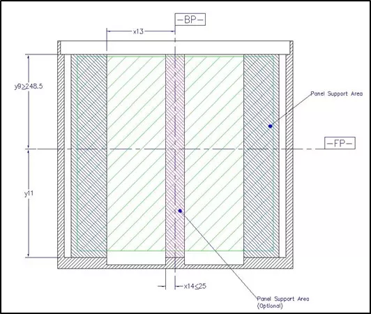
Figure 4 Panel Support Area
Specifications for automation flanges such as OHT (Overhead Transfer) can be found in the appendix of each subordinate document. In addition, the position of the center of gravity is also specified in order to stably transport the panel FOUP, which will exceed 40 kg at the maximum.
At the End
Load Port / EFEM standards for panel FOUP will also be published this summer. And the first edition of the Panel FOUP Standard has been published, but will continue to be revised as needed due to feedback from the industry. We welcome those who are interested to participate in the development activities of the SEMI standard.
About the Authors
Shoji Komatsu (CEO, Acteon NEXT LLC) has been involved in developing SEMI Standards for 20 years. Mr. Shoji Komatsu currently Technical Architect the Japan Physical Interfaces & Carriers Technology Committee and leads the Panel Level Packaging Panel FOUP Task Force.
Get Involved
SEMI Standards development activities take place throughout the year in all major manufacturing regions. To get involved, join the SEMI International Standards Program at: www.semi.org/standardsmembership.
For more information, please visit our main Web site and current events page. If you have any questions regarding SEMI Standards activities, please contact your local SEMI Standards staff.
Standards Watch
SEMI
www.semi.org
June 3, 2021