Standard for Substrate Mapping Recently Updated
By Michelle Sun, SEMI
SEMI E142, Specification for Substrate Mapping, has been recently revised to include additional substrate types and new traceability features.
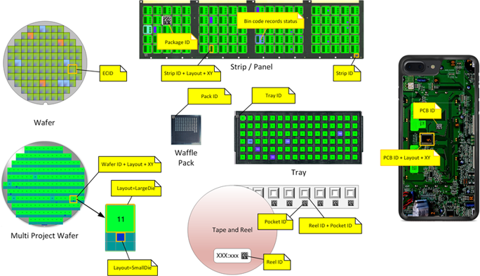
The Standard provides a way to report, store and transmit substrate maps between semiconductor manufacturing sites by describing the layout of devices on a substrate. The substrate types were originally limited to wafers, strips and trays. However, devices are often processed, transported or assembled on other mediums and form factors. The update defines additional substrate types, including tape and reel (TnR) and printed circuit boards (PCB), and describes how the physical substrates can be aligned with SEMI E142 map data.
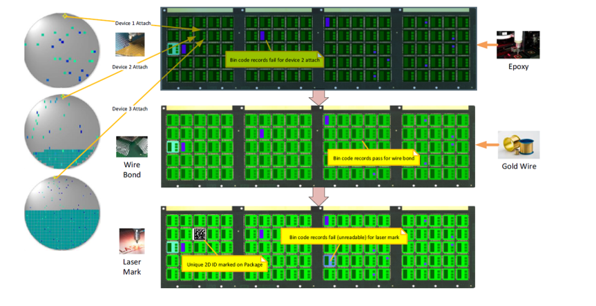
At the same time, package and board assembly has become more complex and plays an increasingly important role in the quality and reliability of the final device. As a result, there is a need to trace raw materials and certain process variables in addition to the die in the package. The update adds device level raw materials and process variable traceability to the existing die traceability in SEMI E142. This can help assembly and packaging companies control their product quality.
The next revision will further expand upon the framework describing the hierarchical layout of complex electronic assemblies. It will add an attribute to the layout object, which could allow users to trace layout paths and identify which ones represent an individual functional package. Use cases include marking entire package if there is a single fail bin for one die. The revision will also create new data transfer methods to accommodate for the addition of DeviceData to SEMI E142.
Identifying Single Devices in the Assembly Flow
Track all MCM components and consumables
This activity is headed by the Advanced Backend Factory Integration (ABFI) Task Force, under the North America Information & Control Technical Committee Chapter, which seeks to develop equipment automation standards for Backend tools (Bump, Chip Probing, Assembly, Final Test and Sensor) to enable full automation, including wafer and die processing tools.
The new revision was recently approved at the SEMI Standards Information & Control Taiwan Technical Committee Chapter Meeting in July and is now available for purchase on the SEMI website or SEMIViews.

Get Involved
SEMI Standards development activities take place throughout the year in all major manufacturing regions. To get involved, join the SEMI International Standards Program at: www.semi.org/standardsmembership.
For more information please visit our main Web site and current events page. If you have any questions regarding SEMI Standards activities, please contact your local SEMI Standards staff.
Standards Watch
SEMI
www.semi.org
September 10, 2020