
Japan Panel Level Packaging Standards Development Highlights
By Masahiro Tsuriya (iNEMI), Haruo Shimamoto (AIST)
3DP&I Japan Technical Committee (TC) Chapter has developed the advanced packaging technology such as fan-out WLP (FOWLP) and Panel Level Packaging (PLP) in addition to the legacy packaging technologies. Inputs and recommendations have received from the industries when panel discussions have performed at SEMICON Japan. The focused areas for the discussions are more on the packaging materials, equipment and metrologies through the advantage of the members professional areas. Below is the overview of PLP related standard development activities in Japan.
WLP/PLP Encapsulation Characteristics Task Force
This Task Force (TF) kicked off in October 2019 and plan to submit a ballot in 2021. Several types of encapsulation materials are used for WLP and PLP, which are granule, sheet and liquid type. The encapsulation process varies based on the encapsulation materials. See Figure 1 below.
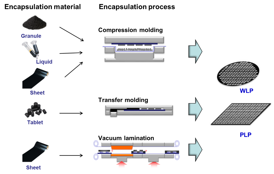
Figure 1 Encapsulation Materials and Process
Mold resin material characteristics are specified for legacy packages such as leadframe package and BGA packages, but there is no specification for encapsulation characteristics for FOWLP and PLP. PLP encapsulant can be used different types and the characteristics between PLP and BGA/Leadframe packages are required differently.
This TF has been developing the measurement/testing method for key material characteristics. Key characteristics are wettability, gel time, CTE, Tg, flowability, modulus, viscosity, and shear strength (shear and peel).
This TF is also working on the development of PLP panel warpage and total thickness variation (TTV) measurement methods. In order to cope with the minimization of line width, it is necessary to reduce the depth of focus of the exposure beam as the exposure beam NA increases. When the target line width is 1 um, lens NA0.4 is required, and the depth of focus is 2 um. So, the measurement metrology is a key to understand the encapsulated panel surface roughness, warpage and TTV to achieve finer RDL (re-distribution layer). For further information, please contact Masahiro Tsuriya ([email protected]).
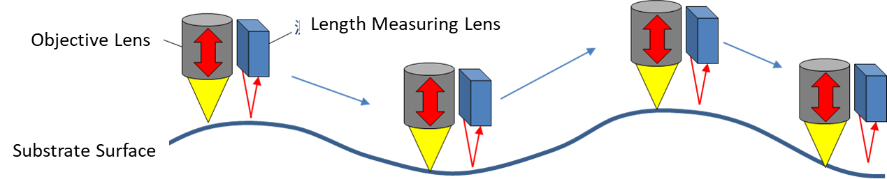
Figure 2 Panel Surface Topology
Panel Level Packaging (PLP) Glass Carrier Task Force
Glass substrate is commonly used to carry a PLP Panel during the processes as glass has superior material properties of optical transparency, coefficient of thermal expansion tunability, high elastic modulus and surface smoothness, comparing with other material of plastic and metal. Key advantage of the glass carrier substrate is debonding technology by laser at temporary bonding and debonding process which enable to minimize thermo-mechanical stresses. This TF will develop Document 6590, Specification for Glass Carrier Characteristics for Panel Level Packaging Applications, and is working jointly with the Panel Level Packaging (PLP) Glass Carrier ID Marking Task Force under the Traceability Japan TC Chapter and PLP Panel FOUP TF team. The plan is to submit to voting in Cycle 8-2020. For further information, contact Mark Takahashi ([email protected]).
The specification items are as follow:
- Substrate size, thickness, edge condition, squareness, surface roughness, warp, TTV
- Orientation corner
- ID mark location (ID mark itself will be specified by PLP Glass Carrier ID Marking Task Force under the Traceability Japan TC Chapter)
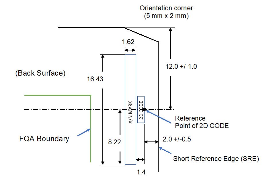
Figure 3 ID Mark Location
3DS IC Bonded Layer Inspection Metrology Task Force
This TF is working on the development of a standard and/or guideline for 3DS-IC defect inspection metrology. Below are items to be specified in the document:
- Voids detection by Scanning Acoustic Microscopy (SAM)
- Multi Wafer/Die stacked more than two
- Stacking method are w/wo adhesive material and some other items
Existing standard SEMI 3D17, Specification for Reference Material for Bonded Wafer Stack Void Metrology, describes the detailed specification of reference bonded wafer. There are several manufacturing processes for Bonded Water Stack and structure, then several types of voids are generated between the bonded wafers.
This TF kicked off in November 2019 to make the guideline to separate the boundary of several bonded wafers (see Figure 4) for the multi stacked wafers. The task force evaluates the inspection capability on the evaluation stacked wafers sample and plan to submit the ballot early next year. This standard will be including the items as below. For further information, please contact Haruo Shimamoto ([email protected]).
- Specification of identification mark size and feature)to separate stacked wafer
- Metrology of defect inspection(Probe selection guideline, etc.)
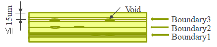
Figure 4 Example of 4-layer wafer stacked Sample
The 3D P&I Japan TC Chapter has collaborated with the Taiwan TC Chapter and has identified the possible areas of SEMI for PLP application as to accelerate the PLP market penetration.
Please contact Mami Nakajo/SEMI Japan ([email protected]) about 3D P&I Japan TC Chapter.
Get Involved
SEMI Standards development activities take place throughout the year in all major manufacturing regions. To get involved, join the SEMI International Standards Program at: www.semi.org/standardsmembership.
For more information please visit our main Web site and current events page. If you have any questions regarding SEMI Standards activities, please contact your local SEMI Standards staff.
Standards Watch
SEMI
www.semi.org
September 10, 2020