
SEMI Building Information Modeling Task Force Reenergized
By Laura Nguyen, SEMI
Within the semiconductor industry, the diversity and complexity of manufacturing equipment creates difficult challenges for facilities design and equipment installation. The need for semiconductor manufacturers to reduce installation time and associated cost, and to optimize their facilities through modeling has led to the need for a standard format and utility data consistent with other SEMI Standards.
This is the latest trend in facilities planning. Building upon on other SEMI Standards, such as SEMI E6 , E51 , E70 , and E72 as a guide, this document creates a standard BIM model format referred to as a Facilities Data Package (FDP). Within the FDP is a 3D model (shell only) of a given piece of equipment with utility points of connections and/or interconnect information (water, power, gas, exhaust, etc.) defined in the model. The model needs to reflect the true dimensions of the equipment and show the x, y, and z location of each interface point.
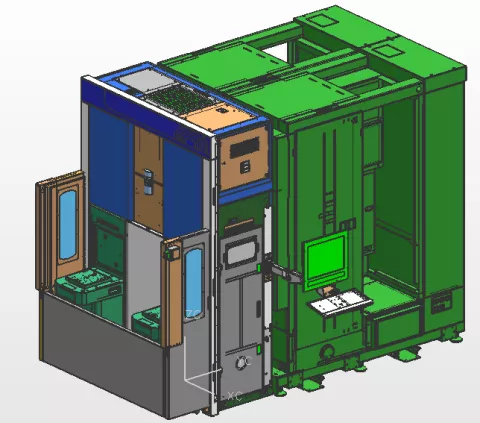
Sample of 3D Model Shell
It is also expected to contain utility information about idle, typical, and maximum usage of each interface point currently defined in SEMI E6, Guide for Semiconductor Equipment Installation Documentation. This allows the user to build virtual models and digital twins of their entire fab, optimize layouts, and plan all of the facilities requirements, including facilities systems and equipment interconnections routing and sizing. BIM is a major benefit to the semiconductor manufacturers (Fab Owners), engineers, and equipment manufacturers when planning and designing new fabs or optimizing existing fabs. This effort is supported by some of the largest players in the semiconductor manufacturing supply chain.
With a common input format that works for all semiconductor manufacturers and all BIM software, equipment suppliers will only have to create one input dataset for each equipment configuration. The BIM software can then use this input to create the BIM model requested by the semiconductor manufacturers. It can take several hundred-man hours to build such a model and this would become impractical without a common format.
The SEMI BIM for Semiconductor Capital Equipment Task Force , part of the Facilities North America Technical Committee Chapter, was formed to gather input from semiconductor manufacturers, equipment suppliers, and architecture/engineering/construction (AEC) service providers to create a common format for BIM software.
Semiconductor manufacturers that don’t currently plan on using a BIM model will find the FDP more useful than previous information because it contains more details necessary to install the equipment.
The Task Force’s initial proposal, SEMI Draft Document 6628: Guide for Facilities Data Package for Semiconductor Equipment Installation, will benefit equipment suppliers and semiconductor manufacturers by communicating, in a standardized way, the information necessary to prepare, optimize and model the facility, and to efficiently install semiconductor equipment.
Get Involved
The next SEMI BIM Task Force meeting, led by Exyte, will be held August 3, 2020, during the North America Standards Summer Meetings via Web conference. Be sure to check https://www.semi.org/standards-events for the latest schedule.
The Task Force welcomes anyone who is interested to participate, especially equipment suppliers, semiconductor manufacturers, architecture/engineering/construction (AEC) service providers. To attend these meetings you must be a SEMI Standards Program Member. Make sure your company influences the development of Standards critical to the industry! Become a SEMI Standards Program Member at www.semi.org/standardsmembership.
For more information please visit our main Web site and current events page. If you have any questions regarding SEMI Standards activities, please contact your local SEMI Standards staff.
Standards Watch
SEMI
www.semi.org
June 11, 2020