
Current Standardization Activity for 300 mm Tape Frame FOUP and the Physical Interfaces
By Hayato Iwamoto, Sony Semiconductor Solutions

Co-leader of 300 mm Tape Frame PI&C Task Force under the Japan TC Chapter of Physical Interfaces & Carriers (PI&C) Global Technical Committee
Background: Where this Activity Started
Currently, 300 mm wafer retained on the tape frame (i.e., wafer tape frame) is placed in the open cassette and transferred at the back end of the process line. Cleanliness requirements become severe as process shrinks and requirements on quality at the back-end process become higher. Back-end process also requires the mini-environment similar to the one used at the front-end process to ensure the device quality. Standardizing the mini-environment carrier (FOUP) for 300 mm tape frame and its physical interface are needed to utilize development and design effort as semiconductor industry.
The 300 mm Tape Frame PI&C Task Force was formed under the Japan Technical Committee Chapter of the PI&C Global Technical Committee in July 2018. SEMI Standard 300 mm FOUP, which is widely used in the front-end process, is not enough for diameter size, so new standard documents are required.
Document Development
With the leadership of Sony Semiconductor Solutions and TOKYO SEIMITSU, a lot of discussion has been taken place in the development of the document.
At the start of this activity only 12 people from 7 companies in Japan were actively participating. As the discussion progressed, more and more companies have joined, and today the task force makes up of more than 60 members from about 30 companies such as device manufacturers, foundries, OSAT, and equipment suppliers. They participate in the discussion from the US,Taiwan, and Japan via Web conferencing.
In order to shorten the time to reach the global consensus, the task force has been utilizing existing SEMI Standards for door interface and positioning interface for 300 mm silicon wafer such as SEMI E57 and SEMI G74 to develop these new standards.
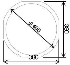 |
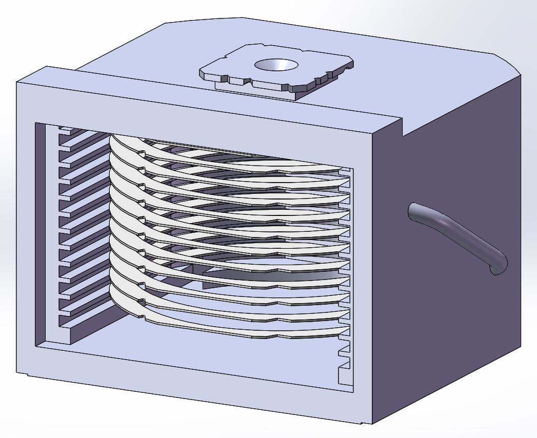 |
View of the 300 mm Tape Frame and FOUP
Since the kick-off meeting in August 2018, the task force has held over 20 meetings, regularly once a month and recently twice a month for the past three months.
At the PI&C Japan TC Chapter meeting held December 2019 in conjunction with SEMICON Japan 2019, the following 5 Standards New Activity Report Forms (SNARFs) were approved after the review by the Global TC members.
- SEMI Document 6521: New Standard, Specification for 300mm Tape Frame FOUP Load Port
- SEMI Document 6522: New Standard, Specification for BOLTS of 300mm Tape Frame FOUP Load Port
- SEMI Document 6523: New Standard, Specification for Front Opening Interface between 300mm Tape Frame FOUP and Load Port
- SEMI Document 6524: New Standard, Specification for Indicator Placement Zone and Switch Placement Volume of 300mm Tape Frame FOUP Load Port
- SEMI Document 6617: New Standard, Specification for 300mm Tape Frame FOUP
Plans for Ballot Submission
SEMI Draft Document 6617: New Standard, Specification for 300mm Tape Frame FOUP, is the first of the five documents above to be issued for voting in Cycle 5-2020. The last day for voting is July 1st. All industry segments involved are invited to review the ballot and vote. Please submit your vote here.
After the global consensus is reached and approved for Ballot 6617, the FOUP for 13 tape frames, a new proposal will be submitted to add an option of FOUP for 25 tape frames to the document.
The task force have begun working on the other four documents for load port and plan to submit the ballots for the Fall 2020 voting cycle.
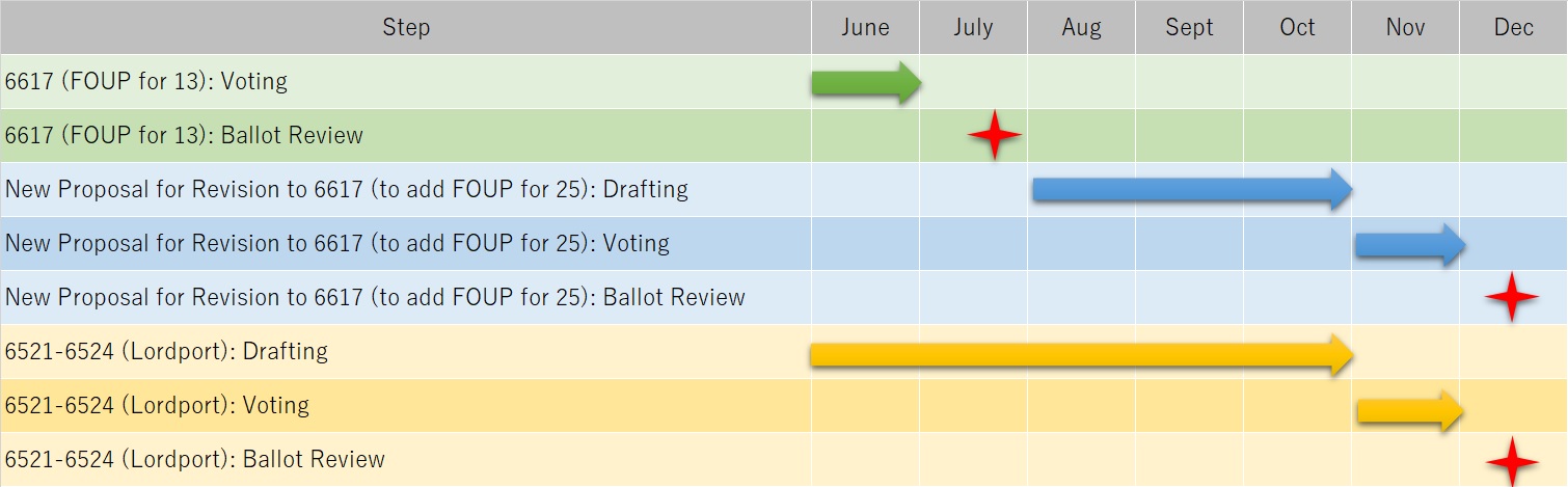
Roadmap for 300 mm Tape Frame Standards
Get Involved
SEMI Standards development activities take place throughout the year in all major manufacturing regions. To get involved, join the SEMI International Standards Program at: www.semi.org/standardsmembership.
For more information please visit our main Web site and current events page. If you have any questions regarding SEMI Standards activities, please contact your local SEMI Standards staff.
Standards Watch
SEMI
www.semi.org
June 11, 2020