
New SEMI Standard for Chemical Mechanical Planarization Pad Hardness
By Alexander Tregub, Intel Corp and Laura Nguyen, SEMI
IC manufacturing is a sophisticated multistep process where parameters need to be monitored and controlled very tightly. Chemical-mechanical polishing (CMP) is an important step in IC manufacturing that is required to achieve global and local planarity for subsequent lithography processes. CMP has been one of the fastest-growing segments of the semiconductor industry for the past 20 years.
The CMP process is highly critical for achieving sustainable yields in IC manufacturing. This area is also one of the most difficult to control. Quality issues in the CMP process are extremely expensive and can have a significant impact to device yields and reliability. It is known that CMP consumables, such as CMP pads, CMP slurries, and CMP conditioning disks are critical to achieve the target performance in IC manufacturing processes. As such, reducing the variations in CMP consumables properties through standardized metrology tools and processes has become a high priority for advanced IC manufacturing nodes.
In this article, we will focus on CMP pads, one of the most critical and widely used consumables in the CMP industry. Specifically, we will review optimization of the measurements and reporting of CMP pad hardness, an important quality parameter that determines removal rate (Figure 1), [Ref. 1], and defectivity of the layer being planarized.
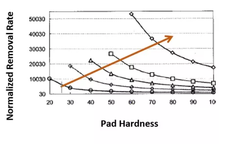
Figure 1. Pad hardness determines Material removal rate, MRR. MRR increases with pad hardness, per most experimental data and models [Ref. 1]
However, CMP pad hardness is not always measured and reported in a consistent way, does not always specify important test conditions, and sometime relies on outdated metrologies. In addition, the effect of temperature on CMP pad hardness (Figure 2) is not always taken into account for reported parameters.
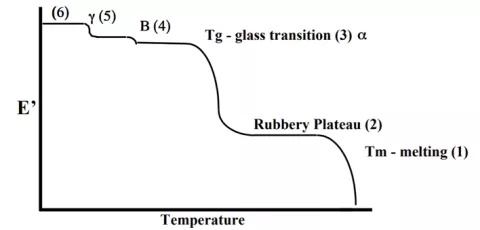
Figure 2. Temperature affects hardness of polymer-made pad. An idealized Dynamic Mechanical Analysis (DMA) scan for storage modulus E’ of a polymer shows decrease of pad hardness, measured as storage modulus E’, with the temperature.
Outdated and inconsistent metrologies employed to measure and report pad hardness result in quality issues and reduced yield in the Fabs, consumable rejects, availability issues, and lack of correlation between reported pad hardness and Fab performance. Until now, there have been no industry-wide consensus Standards for reporting pad hardness.
To close this gap, a group of industry CMP experts partnered with the SEMI International Standards Program, to utilize its reputation for bringing together industry stakeholders to work towards developing globally accepted technical standards, to develop the first suite of SEMI Standards focused on CMP consumables metrology.
Specifically, these new standards will address critical CMP slurry and post-CMP measurements. SEMI C96, Test Method for Determining Density of Chemical Mechanical Polish Slurries, is the first document in the series devoted specifically to CMP slurry users, IDMs, slurry suppliers, metrology manufacturers and OEM equipment suppliers.
The Chemical Mechanical Planarization Consumables (CMP-C) Task Force under Liquid Chemicals Global Technical Committee within the SEMI Standards Program has been actively developing the next SEMI Standard: Guide for Reporting Chemical Mechanical Planarization (CMP) Polishing Pads Hardness used in Semiconductor Manufacturing, report hardness of CMP pads [Ref. 2]. The ballot was recently approved and published as SEMI C100. With more parameters under consideration, CMP pad density [Document 6646] and disks [Document 6677], are under development. Currently, Document 6646, New Standard: Guide for Reporting Density and Porosity of the Chemical Mechanical Planarization (CMP) Pads used in Semiconductor Manufacturing, is out for voting in Cycle 9-2020. Vote today!
Per the new Guide, Dynamic Mechanical Analysis (DMA) metrology is recommended to measure pad hardness. DMA metrology is both more accurate than historical Hardness Shore metrology and measures the effect of temperature on pad hardness [Ref. 3]. The new guide recommends reporting DMA test parameters in a consistent way, such as reporting mode of deformation, load oscillation frequency and amplitude, sampling frequency, coupon preparation procedure, coupon orientation with regard to the pad grooves [Ref. 4], specifying need to report DMA parameters at, at least, 3 temperatures, and other test conditions, as described in Ref. 2. The new guide encourages CMP pad suppliers to continue reporting historic parameter Hardness Shore, to enable continuation of comparisons to the historic databases.
Get Involved
SEMI Standards development activities take place throughout the year in all major manufacturing regions. To get involved, join the SEMI International Standards Program at: www.semi.org/standardsmembership.
For more information, please visit our main Web site and current events page. If you have any questions regarding SEMI Standards activities, please contact your local SEMI Standards staff.
References
- Jianfeng Luo, David A. Dornfeld: IEEE Transactions on Semiconductor Manufacturing, Vol. 14, No. 2, May 2001.
- Guide for Reporting Chemical Mechanical Planarization (CMP) Polishing Pads Hardness used in Semiconductor Manufacturing, SEMI C100, published in November 2020.
- A. Tregub, G. Ng, J. Sorooshian and M. Moinpour, "Thermoanalytical characterization of thermoset polymers for chemical mechanical polishing," Thermochimica Acta 439, pp. 44-51, 2005
- A. Tregub, M. Moinpour and J. Sorooshian, “Effect of Groove Orientation on Thermal and Mechanical Properties of CMP Polishing.” Proceedings of CMPUG Annual Symposium, October 11, 2001, San Jose, CA.
Standards Watch
SEMI
www.semi.org
December 3, 2020