
By Ilona Schmidt, Corning and Richard Allen, NIST
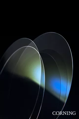
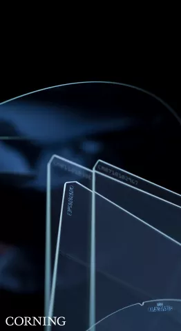
SEMI recently published a new standard SEMI 3D21, Guide for Describing Glass-Based Material for Use in 3DS-IC Process. Non-silicon, dielectric materials have proven to be a valuable alternative to silicon in the semiconductor and 3DS-IC packaging industry. With their unique properties, non-silicon substrates are in use as carrier wafers, spacers, interposers, MEMS, RF devices, and lenses.
However, until now, little information about the features and characteristics of such base materials was available to the industry. This Guide closes the gap for glass as base material in a wide range of semiconductor and 3D-IC applications, including the use of a glass base material in a temporary bonding process, where the glass is used to support a thin wafer during processing. It also covers glass material intended for use as a wafer stack, where the application may include RDL (redistribution layer), TGVs (through glass vias), passive devices, and/or other device elements. The Guide describes dimensional, physical, and thermal characteristics of glass as a base material and refers to adequate test methods and procedures.
This Guide compliments the other SEMI Standards related to glass material for 3D-IC applications below:
- SEMI 3D2, Specification for Glass Carrier Wafers for 3DS-IC Applications
- SEMI 3D11, Terminology for Through Glass Via and Blind Via in Glass Geometrical Metrology
- SEMI 3D16, Specification for Glass Base Material for Semiconductor Packaging
Get Involved
The next 3DP&I Technical Committee meetings will be held in in conjunction with the North America Standards Spring 2020 Meetings held March 30-April 2. There is no cost to attend these meetings, but registration is required. Registration opens early 2020.
Make sure your voice is heard and your company influences the development of the SEMI Standards that are critical to the industry by becoming a SEMI Standards Program Member. To get involved, join the SEMI International Standards Program at: www.semi.org/standardsmembership.
For more information please visit our main Web site and current events page. If you have any questions regarding SEMI Standards activities, please contact your local SEMI Standards staff.
Standards Watch
SEMI
www.semi.org
December 5, 2019
Source Image: © 2019 Corning Incorporated. All Rights Reserved.