downloadGroupGroupnoun_press release_995423_000000 copyGroupnoun_Feed_96767_000000Group 19noun_pictures_1817522_000000Member company iconResource item iconStore item iconGroup 19Group 19noun_Photo_2085192_000000 Copynoun_presentation_2096081_000000Group 19Group Copy 7noun_webinar_692730_000000Path
Skip to main content
Default Banner Image

SEMICON Europa

The Executive Forum at SEMICON Europa in Munich on November 16 was a welcome opportunity to demonstrate the strategic importance of our vital industry.Executives across the entire electronics and applications value chain rightly pointed out the contribution that the semiconductor supply chain made to supporting the efforts to control COVID-19, which sparked explosive demand for semiconductors and led to the chip shortage and supply chain disruptions. The pandemic has heightened the urgency to establish the manufacturing capacity needed to support the global recovery and onward rapid growth of the semiconductor industry, which is projected to exceed $1.2 trillion in revenue by 2030.Semiconductors are the heartbeat of the way we work and live, and their vital importance is now recognized by governments worldwide including European Commission officials, as well as by the wider population.So far, so good. However the rapid industry growth brings opportunities and challenges. If we continue on the path we are now on, there will simply not be enough energy in the world to feed our data appetite in the so-called 5th wave of digital expansion. Many speakers at SEMICON Europa referred to the importance of sustainability and diverse skills, and many companies have put in place comprehensive programmes that will enable industry growth and lead toward net zero carbon emissions. The semiconductor industry is central to efforts to control climate change. Collaboration and cooperation across the European microelectronics ecosystem are essential.Europe is a world leader, and many stunning advances in technology have resulted from many collaborative projects, large and small, over the years. Many of the executives at SEMICON Europa stressed that these efforts must continue, and indeed be expanded, across the entire electronics and applications value chain. However, the focus remains on ever more capable technologies to match the needs of the digital age: data management, communications, computing capability and improving important application areas such as healthcare.(Clockwise) Laith Altimime, president of SEMI Europe; Luc Van den hove, president and CEO of imec; and Lars Reger, Executive VP and CTO of NXP Semiconductors present at SEMICON Europa 2021. But where are the programmes to drastically reduce carbon emissions and air pollution, eliminating the use of scarce resources and acting as a catalyst to keep 1.5 alive? SEMI is doing its part by establishing a sustainability initiative. To help the industry building the talent pipeline crucial to its future growth, SEMI has also developed workforce diversity programs. Both initiatives are bringing together leaders from across the semiconductor supply chain to address these critical challenges. These changes require major disruptions. Time and again, our industry has demonstrated that it can overcome tremendous challenge.Of course, many chip companies are already devoting significant time and effort to help meet the moment, and projects are underway across our industry focused on these great causes. Yet, we can’t rely on individual efforts to fix these global problems. Our industry, with so much capability and history of rapid innovation, needs to take the lead in changing the way we meet these industrial and social imperatives.Contact [email protected] to learn more about the SEMI Environmental, Health, Safety Sustainability initiative and help the semiconductor industry take action today.Learn more about SEMI Diversity and Workforce Development initiatives.Peter Connock is Chair of SEMI Europe Industry Strategy Symposium Committee and Chairman of memsstar Limited.Serena Brischetto is senior manager of Marketing and Digital Engagement at SEMI Europe.
Read More
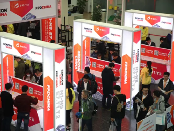
For the second straight year, SEMICON China, among the world’s largest and most influential semiconductor industry events, was the first local tradeshow of its scale held in-person, reflecting China’s rising prominence in the semiconductor industry. After securing approval from the Chinese government to hold large events, SEMI staged SEMICON China 2020 and 2021 with advanced protections against COVID-19 in place. There were no reported infections at either event. Highlights from SEMICON China 2021: Large Scale: Attendance of over 92,000, including more than 66,000 visitors and 25,000 exhibitors. Expo hall totaled 84,500 square meters with about 1,100 exhibiting companies and over 4,000 booths. World-Class Thought Leaders: Strong industry support from key foundries, OSATs, equipment and materials suppliers. Keynote speeches featured world-class industry leaders and head of China’s IC industry fund and global investment consulting agency, who explored the latest global business, technology and market trends and hot domestic investment topics. Concurrent Forums: Forums included SIIP China: SEMI Innovation Investment; Smart Manufacturing; Advanced Manufacturing; Advanced Packaging; Memory; Power Compound Semiconductor; China Display Conference; the all-new Advanced Materials Forum; and China Semiconductor Technology International Conference (CSTIC). Rich Digital Content: SEMICON China’s digital platform provided a rich array of content to attendees around the world including the Grand Opening Keynote and CSTIC, which were broadcast live online. Workforce Development: SEMI China worked closely with industry and government partners to promote SEMI Workforce Development programs to help attract and retain talent for China’s semiconductor industry. SEMICON China again featured the SEMI Workforce Pavilion and SEMI Workforce CXO Talent Forum. Outstanding COVID-19 Protective Measures: SEMICON China deployed advanced testing and monitoring equipment and implemented strict COVID-19 preventative measures to ensure a safe environment for all attendees to network and conduct business. Looking Ahead With the resounding success of SEMICON China 2021, optimism is growing that more physical events will be held with travel restrictions set to ease later this year. The more than 2,500 SEMI members around the world are eager to again network and collaborate face-to-face with customers, suppliers and partners to solve challenges in the microelectronics industry and drive semiconductor innovation that continues to transform how we work and live. That very innovation made many businesses more resilient as the virus spread and enabled people worldwide to work, learn, and shop from home. As SEMI starts to stage other events in-person, we will put in place advanced protective measures against COVID-19 to ensure the safety and well-being of all attendees. As the vaccination roll-out continues worldwide and new COVID-19 strains emerge, SEMI’s flagship SEMICON events are evolving in several ways, most notably with a larger digital presence. In this new era, we offer an international platform for SEMI members and partners across the microelectronics supply chain to collaborate, discuss industry trends, solve common challenges, network, and accelerate business growth through physical, virtual, and hybrid formats. Hybrid events – on-site exhibitions and conferences featuring a digital presence – allow the face-to-face connections so important to the semiconductor industry but also improve the attendee experience by offering an online option with the following benefits: More international accessibility to content live or on-demand Robust interactivity with live-streamed events, allowing more people to participate Greater cost effectiveness to enable companies and people under tight budgets to take advantage of world-class content, including keynote presentations, panel discussions, and technical sessions. In a recent survey of advanced manufacturing businesses, Informa Markets, a multinational publishing, business intelligence, and exhibitions group, found that 93% of respondents are likely to return to in-person events between August and December 2021, signaling a widespread eagerness for the return of live events and face-to-face connections. 
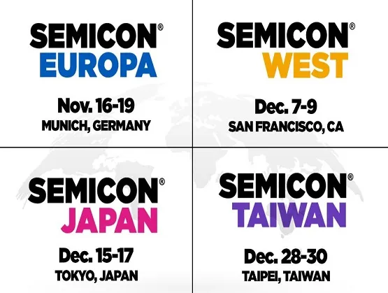
SEMICONs Scheduled for 2021 In a normal year, each of the seven regions where SEMI operates stages a SEMICON, with the exhibitions spread throughout the year. With the world continuing to combat COVID-19, more SEMICONs have been moved to the second half of 2021 – most of them with a hybrid format so exhibitors and attendees can take advantage of the increasing popularity of online events. After last year’s disruptions to the SEMICON schedule – and with more experience in the new normal – SEMI is excited to welcome the businesses and peers who couldn’t attend the 2020 events back to the in-person and hybrid shows. Innovation never sleeps. And SEMI will continue to evolve its events to help you form the partnerships and make the connections vital to the growth of your company and the industry. For more information about regional SEMICONs, please visit the SEMI events page. About the Author David Ghodsizadeh is the Director of Global Product Marketing at SEMI, where he develops customer-centric strategies to market SEMI Membership, Market Data, Expositions, Smart Initiatives, and Technology Communities to members, partners, and industry peers. Connect with David on LinkedIn.
Read More
Artificial intelligence and machine learning are reshaping electronic system design as consumer-facing companies like Facebook and Google design their own hardware. Electronic system design is enabling rapid changes and new innovation in automotive. Designing microchips for the commercialization of outer space faces stiff challenges.These are just a few topics that companies driving technology innovation in electronic system design will discuss at SEMICON Europa, 12-15 November 2019 in Munich, Germany. In the run-up to the event, SEMI spoke with Bob Smith, executive director of the Electronic System Design (ESD) Alliance, a SEMI Strategic Association Partner, about how the integration of the ESD Alliance with SEMI’s global platforms is extending design expertise in the worldwide electronics industry. Smith shared his views ahead of the SMART Design Forum, 14 November 2019, 14:30 to 17:00, at SEMICON Europa. Registration is open. Join the forum to meet experts from ESD Alliance and other key industry influencers. Attendance is free of charge for all SEMICON Europa visitors (Hall B1, TechARENA 1).SEMI: In August of last year, SEMI announced the ESD (Electronic System Design) Alliance joined SEMI as a Strategic Association Partner. How does this partnership benefit the design and semiconductor industries?Smith: As indicated back then by Ajit Manocha, president and CEO of SEMI, “Design is the very foundation of semiconductor innovation and manufacturing.” The integration of the ESD Alliance with SEMI’s event and global platforms enables the design community to expand its expertise to the worldwide electronics industry. The integration helps streamline collaboration and connection of SEMI members with the electronic system design, IP and fabless communities.ESD Alliance members are now able to more efficiently engage with the electronics manufacturing supply chain on technical and business issues and gain access to comprehensive global resources and platforms. Those resources include SEMI’s technology communities and activities in areas such as advocacy, international standards and environment, health and safety (EH S), industry statistics, trade and regulatory initiatives.SEMI: And what were the main opportunities for the ESD Alliance to present the scope of the brand-new collaboration? How did the ESD Alliance enlarge the scope of the semiconductor and design industries?Smith: Although the ESD Alliance has international member companies, the reach and focus of our activities was limited to North America. SEMI’s global platform allows us to spread our design initiatives worldwide. In 2019 we introduced design at SEMICON events in China, Taiwan, the U.S. and now Europe with our participation in SEMICON Europa’s SMART Design Forum. By introducing design into these global events, we are advancing SEMI’s expanded mission to represent the entire global electronic design and manufacturing chain and tighten the connection between the semiconductor and design industries.Industrywide events like SEMICON Europa and its SMART Design Forum bring the entire electronic product supply chain closer together by focusing on commercial achievements in design and presenting forward-looking, system-centric views. The Smart Design Forum is a great opportunity for attendees to deepen their understanding of the links across design and manufacturing and throughout the supply chain during sessions and informal discussions at networking and social events. These exchanges help foster the collaborations essential to addressing technical challenges and ushering exciting new electronic products from concept to consumer.SEMI: How is the semiconductor design ecosystem evolving? What disciplines are becoming integrated with those that have historically governed the scene? Can you tell us more about the concept of system-centric view?Smith: In the early days of electronic design automation (EDA), design was largely separated from manufacturing. On the design side, the goal was to design and tape-out chips. After tape-out, the chip was handed off to the manufacturing group and the design team went on to a new project. We refer to this era as chip-centric.Now, given the complexity of both chips and electronic systems, design and manufacturing can no longer be separated. Instead, they must collaborate from the beginning of a project on all aspects of system design. This system-centric view enables the delivery of smarter, faster, more powerful, and more affordable electronic products. This is a big responsibility and meeting it demands tight cooperation and collaboration across multiple disciplines including semiconductor design, packaging, software development, materials and manufacturing, system integration and testing.SEMI: What’s one of your strategic objectives for 2020? Smith: In 2020 we plan to launch our Connecting the Divide initiative to bring the design and manufacturing communities closer together to help both better understand the role of the other, the value each provides and the unique challenges each community faces. The goal is to increase the rate of collaboration between design and manufacturing in answering both industries’ need for a system-centric approach to new electronic product/system design.SEMI: Do we have good reason to be optimistic about opportunities on the horizon? What’s one prediction for the future of semiconductor design solutions you’d like to share?Smith: We seem to be surrounded by almost limitless opportunities. In terms of design, my prediction is that we will see higher levels of system design abstraction that will allow systems to be rapidly configured and verified in a way that we cannot do today. In essence, we will be able to build virtual systems rapidly to reduce the risk and cost of developing new electronic products.SEMI: What are your expectations regarding the SMART Design Forum at SEMICON Europa 2019 in Munich? Smith: We are excited to be bringing the design conversation into SEMICON Europa at the SMART Design Forum. Europe has been recognized as a leading region in embracing and driving system design. Our objective is to move deeper into system-centric design through the exchange of information and ideas at the SMART Design Forum.Robert (Bob) Smith is Executive Director of the Electronic System Design (ESD) Alliance, a SEMI Strategic Association Partner. The ESD Alliance is an international trade association of companies providing goods and services throughout the semiconductor design ecosystem. Bob began his career as an analog design engineer at Hewlett-Packard working on disk drive technology. Since then, he has spent more than 30 years in various roles in executive management, marketing, and business development primarily working with startup and other early stage companies in Electronic Design Automation (EDA) and semiconductor IP. These companies include IKOS Systems, Synopsys, LogicVision, Magma Design Automation and Uniquify. He was a member of the IPO teams that took Synopsys public in 1992 and Magma public in 2001. Bob received his BSEE from U.C. Davis and his MSEE from Stanford University. Serena Brischetto is a marketing and communications manager at SEMI Europe.
Read More