downloadGroupGroupnoun_press release_995423_000000 copyGroupnoun_Feed_96767_000000Group 19noun_pictures_1817522_000000Member company iconResource item iconStore item iconGroup 19Group 19noun_Photo_2085192_000000 Copynoun_presentation_2096081_000000Group 19Group Copy 7noun_webinar_692730_000000Path
Skip to main content
Default Banner Image

Qualcomm

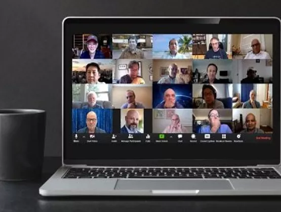
Tracking and quickly diagnosing COVID-19 infections, working from home and telemedicine recently came into sharp focus as technology executives and other subject matter experts from microelectronics heavyweights recently gathered for the first-ever virtual SEMI CTO Forum to explore how the microelectronics industry and their own companies can leverage future technology trends to drive growth. Themed Intelligent Medtech and Wearable Technologies, the forum drew CTOs from ARM, Babblelabs, Brewer Science, Dell, Dow/Dupont, E-Ink, Hewlett Packard Enterprise, Intel, Lam Research, KLA, Microchip, ON Semiconductor, Qualcomm, Tokyo Electron, Ulvac, Veeco and Xilinx. The event is designed as a strategic driver of pre-competitive innovation. Following are key takeaways from the forum. Microfluidics Promises to Speed COVID-19 Diagnosis More than 240 companies worldwide are developing microfluidics solutions to improve diagnosis and treatment of COVID-19 and other conditions, said forum speaker Dr. Kurt Petersen, a member of Band of Angels, Silicon Valley's oldest angel investment group, with an illustrious background1 in technology. And their innovations are bearing fruit. Cepheid, a company founded by Dr. Petersen, has developed a disposable microfluidic cartridge, Xpert Xpress SARS-CoV-2, used by doctors to swab the inside of a patient’s mouth. Highlighting the vital role of MEMS in medical electronics, the tiny powerful devices are behind a test that can detect COVID-19 infection in under 40 minutes. Dr. Petersen also cited a few examples of implantables and injectables under development, including: In vivo chemical sensing: Profusa developed a continuous glucose monitoring sensor via an optical patch. Glaucoma pressure monitors: Injectsense built a silicon chip the size of a grain of rice that is embedded in the eye to measure eye pressure. Retinal implants: Second Sight implanted a 60-electrode array chip that projects images onto the retina to improve vision. Microelectronics Takes Aim at Battling COVID-19 The event’s CTO roundtable, a platform for discussing societal and technology issues, revealed microelectronics technology will likely give rise to solutions for combatting pandemics and new business opportunities both in the short and long run. Areas of the greatest interest included: Tracking and Security: Infection tracking accuracy is key to limiting the spread of viruses yet comes with inherent privacy and security challenges. The consensus view of the executives was that developing trusted hardware capabilities is critical for adoption of accurate infection-tracking technologies. Remote Operation: Executives expect working from home or the use of telehealth to continue building momentum long after pandemic. To give staying power to the remote communications at the heart of these trends, microelectronics ecosystems will need to boost compute performance, both at the edge and in the cloud, while increasing bandwidth to enable applications such as augmented reality/virtual reality (AR/VR), artificial intelligence (AI), machine learning and advanced data analytics. Edge intelligence: The challenge of remote communications spans both people and the Internet of Things (IoT). Questions persist about how hundreds of billions of sensors will connect to the cloud and how much power they will consume. The need to push computing to where data is generated – at the edge – is rising and the necessary underlying technologies will only come by combining various forms of distributed computing and analytics. The microelectronics industry’s ability to seize these opportunities will only be possible with huge strides in innovation, raising concerns among the CTOs about the financial viability of cutting-edge devices because of increasing device complexity and R D costs. Technology partnerships and collaborations – an area where SEMI is contributing and will continue to expand its efforts as it works with the CTO community – will be critical to containing R D costs. SEMI will help the executives identify and mobilize the resources key to future innovation. Improving Home, Work Productivity and Experiences Key to AR Adoption Smart wearables also offer great promise. In just over a decade, AR and VR have grown from science fiction to practical uses such as AR applications for smart contact lenses, said Dr. Mike Wiemer, Co-Founder and CTO of Mojo Vision2. Dr. Wiemer said that while many AR applications remain under development, the technology will only see widespread adoption once it starts to improve productivity and efficiency at home and work and the quality of other experiences. The smart augmented reality contact lens developed by Mojo Vision is a step in that direction. The product’s built-in display gives users timely information about everything they see while remaining invisible by packing 70,000 pixels into a space smaller than a half a millimeter across, making it the smallest and densest dynamic display ever made. The contact lens is powered by an ARM-based processor, with later versions adding an image sensor, eye-tracking sensors and a communications chip. SEMI thanks EMD Performance Materials and Telit for sponsoring the CTO Forum. For more information on the CTO Forum and SEMI’s Smart Data-AI initiative, please sign up on our webpage. 1 Dr. Kurt Petersen is a member of the National Academy of Engineering, an IEEE Medal of Honor winner, and a Life Fellow of the IEEE for his contributions to the commercialization of MEMS technology. 2 Dr. Wiemer also co-founded Solar Junction, where he led technical teams to two world records in solar cell efficiency (43.5% and 44%). He also has patents and papers in Semiconductor Devices Applications, Silicon Photonics, Materials Integration, Lasers, Solar Cells, Solar Systems, and Analog Circuits. Tom Salmon is Vice President of Collaborative Technology Platforms at SEMI. Pushkar P. Apte, Ph.D., is Strategic Technology Advisor for the Smart Data AI Initiative at SEMI.
Read More
For medtech applications to flourish, sensors need a supporting infrastructure that translates the data they harvest into actionable insights, says Qualcomm Life director of business development Gene Dantsker, who will speak about the future of digital healthcare in the Medtech program at SEMICON West. “Rarely can one device give a complete diagnosis,” he notes. “What’s missing is the integration of all the sensor data into prescriptive information.” The maturing medtech sector has developed to the point where sensors can now capture massive amounts of data, conveniently collected from people via mobile devices. The sector now has higher compute capacity to process the data, and improving software can produce actionable insight from the information. The next challenge is to seamlessly integrate these components into legacy medical systems without disrupting existing workflow. “Doctors and nurses don’t have time for disruptive technology – a new system has to be invisible and frictionless to use, with one or fewer buttons, no training and truly automatic Bluetooth-like pairing,” he says. “So device makers need to pack all system intelligence into the circuits and software.”Getting actionable healthcare information from sensors requires integration into the existing medical infrastructure. Source: Qualcomm LifeOne interesting example is United Healthcare’s use of the Qualcomm Life infrastructure to collect data from the fitness trackers of 350,000 patients. The insurance company then pays users $4 a day, or ~$1500 a year, for standing, walking six times a day and other behaviors that clinical evidence shows will both improve patient health and reduce healthcare costs. “It’s a perfect storm of motivations for all stakeholders,” he says.Next hot MEMS topics: Piezoelectric devices, environmental sensors, near-zero power standbyWith sensor technology continuing to evolve, look for coming innovations in MEMS in piezoelectric devices, environmental sensors and near zero-power standby devices, says Alissa Fitzgerald, Founder and Managing Member of A.M. Fitzgerald and Associates, who will provide an update on emerging sensor technologies in the MEMS program at SEMICON West.Piezoelectric devices can potentially be more stable and perhaps even easier to ramp to volume than capacitive ones, with AlN devices for microphones and ultrasonic sensors finding quick success. Now the maturing infrastructure for lead zirconate titantate (PZT) is enabling the scaling of production of higher performing piezo material with thin film deposition equipment from suppliers like Ulvac Technologies and Solmates and in foundry processes at Silex and STMicroelectronics, she notes.In academic research, where most new MEMS emerge, market interest is driving development of environmental sensors and zero-power standby devices. With demand for environmental monitoring growing, much work is focusing on technologies that improve the sensitivity, selectivity and time of response of gas and particulate sensors. Research and funding is also focusing on zero or near-zero power standby sensors, using open circuits that draw no power until a physical stimulus such as vibration or heat wakes them up.MEMS, however, likely won’t find as much of a market in autonomous vehicles as once thought. “While the automotive sensor market will need many optical sensors, MEMS players are competing with other optical and mechanical solutions,” says Fitzgerald. “And here the usual MEMS advantage of small size may not matter much, and the devices will have to meet the challenging automotive requirements for extreme ruggedness.”Paula Doe, SEMI
Read More
What’s next for smarter, more connected electronics manufacturing - Part 3 The fast-maturing infrastructure now enabling analysis of exponentially larger data volumes brings the microelectronics industry to an inflection point, where the winning companies will be the first to master the use of this data to solve the industry’s emerging challenges. SEMI expands its coverage of these vital issues with a Smart Manufacturing Pavilion and three days of talks SEMICON West, July 10-12 in San Francisco. While deep learning is starting to be applied to image recognition for wafer inspection, it is also being considered for sequential pattern recognition in order to evaluate equipment parameter traces. The next emerging applications will start to use those learned patterns to predict outcomes, and then use those predictions to automate process control. One early application of deep learning is IC process development. “People don’t think of research and development as the first place to automate, but it’s where applying our digitization and simulation has first had impact,” says David Fried, Coventor vice president of Computational Products. He noted that insertion is easier in the lab than in the fab. Technology at 10nm and beyond is now so complex that companies at the leading edge must use process modeling to understand the effect of process variation on their designs. Learning cycles can now be accelerated during development by simulating 10,000 digital wafers instead of running 25 actual wafers during screening, Fried says. Applying structured analysis and machine learning to the data simplifies optimization across the 500 or more interrelated process steps. Coventor has recently introduced a statistical analysis package that aids the design and analysis of process variation experiments by using large volumes of data from its models. Fried says these models are next being used to accelerate the yield ramp in manufacturing. Digital simulation also could speed development of high-mix, lower value products While digital twins are best known for their use in complex, high value products like jet engines, the simulation technology could also enable the electronic manufacturing services (EMS) sector to reduce the time, cost and risk of developing its high mix of products. “The EMS sector’s use of digital twins will be vital for it to smooth the move of CAD/CAM digital design data for so many different products into manufacturing, and to accelerate validation testing of designs and products by doing more of it in the virtual world,” says Dan Gamota, vice president of Engineering and Technical Services at Jabil. Gamota also highlights the push for traceability from the automotive and healthcare markets, where the digital models could be used to quickly assure that the design was built exactly as specified. “In the past year, traceability has evolved from just ‘nice to have’ to ‘how to achieve,’” he adds. “Companies are expecting it, but aren’t willing to accept the cost and risk of doing it alone. We need the community to discuss realistic implementations, identify the most critical elements and bring together the ecosystem partners to build baseline reference architectures for key digital building blocks. The community also needs to assure the reliable flow of data among the electronic manufacturing segments from semiconductor to OSAT to EMS.” Predictive maintenance and virtual metrology applications could mature in next few years While predictive maintenance initially seemed a likely early application of machine learning in factories, it remains a challenge for the electronics sector. “The difficulty is that it’s not clear where to get the most bang for the buck,” says Tom Ho, president of BISTel America, noting that it may make the most sense to track the failure performance of a single expensive part, like an electrostatic chuck, since predicting the failure performance of a whole complex system like an etcher is much harder. “Collecting enough data from all failure types, including especially the rare events, is difficult unless you have a long history of a lot of tools,” adds Doug Suerich, PEER Group product evangelist. “The gain from collecting performance information from many tools across the industry could be big, but many companies still need to overcome concerns around exposing their IP.” Another big opportunity for prediction is virtual metrology – predicting the wafer outcome from the process or sensor data with enough accuracy to replace the physical metrology. “Virtual metrology is improving, and since metrology can be slow and expensive, any reduction could mean a huge potential savings,” says Suerich. “But it is still seen as too scary for many companies. Two to three years from now, companies will expand the practice from lower risk areas into processes that require more confidence in the results.” Moving beyond prediction to automated control needs digital models Once the results are predicted, the model can be used to control or automatically optimize a process and enable the system to learn by itself, usually by reinforcement learning on a digital model. The model can then independently make adjustments to optimize the manufacturing process. “Automated process development is getting close now. Instead of smart guys turning the knobs, deep learning is automating the smart tuning,” says Suerich, suggesting the industry could see widespread adoption in as little as two to three years. This type of machine learning needs a good digital model, and masses of data for learning. One approach uses human experts to build a physics-based model of the clearly understood parts of the process, then turns to deep machine learning to optimize the lesser-understood variables. The alternative, the data-first approach, runs a computer algorithm to suggest the solution purely from data, without human input, and then relies on the human to evaluate the usefulness of the results. Modeling digital twins of wafers could enable automated process control, chamber matching, and fleet matching, says Fried. If every wafer had its own virtual twin with all the upstream metrology and structural information needed to make equipment control decisions, it could feed forward that information to enable the seamless transition from one step in the process to another based on understanding their complex interrelationships. This could potentially improve uniformity across wafers and equipment, and reduce the need for metrology, he argues. Moving metrology sensors into the chamber will also require model-based algorithms to enable dynamic process control in close to real time, says Fried. These algorithms will be needed to acquire, parse, and process the data at high speed, and then to choose how to adjust the controls. “There will be a model behind collecting and interpreting the metrology data,” he notes. “That’s a really rich vein for improvements in process control.” “The end goal is to collect equipment data in real time, analyze it with AI, and send back controls to optimize manufacturing processes,” Jabil’s Gamota says. “This requires a robust architecture for communication between equipment and consistent formats for data collection and analysis. But the cost and complexity of this heavy lifting is too great for any one company to do alone. We need a consensus-based architecture for ingesting, analyzing and acting on the data.” SEMI tests data transfer protocols, benchmarks best practices SEMI is launching a smart data project to identify the various data transfer protocols needed for inter-company communications. The project will feature a proof-of-concept model in a development fab to produce verifiable results so SEMI can better understand how different approaches meet member needs. SEMI’s smart manufacturing technology communities and the Fab Owners Alliance are also benchmarking current smart manufacturing practices in the microelectronics industry to help SEMI members better understand the path forward and potential return on investment. Speakers over all three days at SEMICON West addressing these issues include Active Layer Parametrics, Applied Materials, Applied Research Photonics, ASML, Bosch Rexroth, Cimetrix, Coventor, ECI Technologies, Edwards Vacuum, Final Phase Systems, GE Digital, Infineon, Jabil, Lam Research, Osaro, Otosense, PEER Group, Qualcomm, Rockwell Automation, Rudolph Technologies, Schneider Electric, Seagate, Siemens, Stanford University, TEL, TIBCO Software. See semiconwest.org. What’s next for smarter, more connected electronics manufacturing - Part 1 What’s next for smarter, more connected electronics manufacturing - Part 2 Paula Doe, SEMI
Read More
With artificial intelligence (AI) rapidly evolving, look for applications like voice recognition and image recognition to get more efficient, more affordable, and far more common in a variety of products over the next few years. This growth in applications will drive demand for new architectures that deliver the higher performance and lower power consumption required for widespread AI adoption. “The challenge for AI at the edge is to optimize the whole system-on-a-chip architecture and its components, all the way to semiconductor technology IP blocks, to process complex AI workloads quickly and at low power,” says Qualcomm Technologies Senior Director of Engineering Evgeni Gousev, who will provide an update on the progress of AI at the edge in a Data and AI program at SEMICON West, July 10-12 in San Francisco. Qualcomm Snapdragon 845 uses heterogeneous computing across the CPU, GPU, and DSP for power-efficient processing for constantly evolving AI models. Source: QualcommA system approach that optimizes across hardware, software, and algorithms is necessary to deliver the ultra-low power – to a sub 1-milliwatt level, low enough to enable always-on machine vision processing – for the usually energy-intensive AI computing. From the chip architecture perspective, processing AI workloads with the most appropriate engine, such as the CPU, GPU, and DSP with dedicated hardware acceleration, provides the best power efficiency – and flexibility for dealing with rapidly changing AI models and growing diversity of applications.“So far it’s been largely a brute force approach using conventional architectures and cloud-based infrastructure,” says Evgeni. “But we’re going to run out of brute force options, so future opportunities lie in developing innovative architectures, dedicated hardware, new algorithms, and new software. Innovation will be especially important for AI at the edge and applications requiring always-on functionality. Training is mostly in the cloud now, but in the near future it will start migrating to the device as the algorithms and hardware improve. AI at the edge will also remove some privacy concerns, an increasingly important issue for data collection and management.”Practical AI applications at the edge where resources are constrained run the gamut, spanning smartphones, drones, autonomous vehicles, virtual reality, augmented reality and smart home solutions such as connected cameras. “More AI on the edge will create a huge opportunity for the whole ecosystem – chip designers, semiconductor and device manufacturers, applications developers, and data and service providers. And it’s going to make a significant impact on the way we work, live, and interact with the world around us,” Evgeni said.Future generations of chips may need more disruptive systems-level change to handle high data volumes with low power A next-generation solution for handling the massive proliferation of AI data could be a nanotechnology system, such as the collaborative N3XT (Nano-Engineered Computing Systems Technology) project, led by H.S. Philip Wong and Subhasish Mitra at Stanford. “Even with next-generation scaling of transistors and new memory chips, the bottlenecks in moving data in and out of memory for processing will remain,” says Mitra, another speaker in the SEMICON West program. “The true benefits of nanotechnology will only come from new architectures enabled by nanosystems. One thing we are certain of is that massively more capable and more energy-efficient systems will be necessary for almost any future application, so we will need to think about system-level improvements.” Major improvement in handling high volumes of data with low high energy use will require system-level improvements, such as monolithic 3D integration of carbon nanotube transistors in the multi-campus N3XT chip research effort. Source: Stanford UniversityThat means carbon nanotube transistors for logic, high density non-volatile MRAM and ReRAM for memory, fine-grained monolithic 3D for integration, new architectures for computation immersed in memory, and new materials for heat removal. “The N3XT approach is key for the 1000X energy efficiency needed,” says Mitra.Researchers have demonstrated improvements in all these areas, including multiple hardware nanosystem prototypes targeting AI applications. The researchers have transferred multiple layers of as-grown carbon nanotubes to the target wafer to significantly improve CNT density and have also developed a low-power TiN/HfOx/Pt ReRAM. The low-temperature CNT and ReRAM processes enable multiple vertical layers to be grown on top of one another for ultra-dense and fine-grained monolithic 3D integration. Other speakers at the Data and AI TechXpot include Fram Akiki, VP Electronics, Siemens; Hariharan Ananthanarayanan, motion planning engineer, Osaro; and David Haynes, Sr. director, strategic marketing, Lam Research. See SEMICONWest.org.Paula Doe, SEMI
Read More
What’s next for smarter, more connected electronics manufacturing - Part 1The fast-maturing infrastructure now enabling applications for big data and artificial intelligence means disruptive change not just at individual companies but also in data connections among companies across the microelectronics manufacturing value chain. SEMI expands its smart manufacturing program with a Smart Manufacturing Pavilion with displays and three full days of talks to address these industry-wide developments at SEMICON West, July 10-12 in San Francisco.Autonomous autos’ demand for zero-defect systems and 100 percent traceability back to the manufacturing data for each die is driving a push to traceability across the chip sector. “Far more chips are being used by the automotive sector, and its very different requirements are driving demand for traceability,” says Tom Ho, president of BISTel America. “Our chipmaker customers are looking for traceability solutions and the trend is the same in backend packaging and assembly – automotive applications are driving the sector to traceability.”Traceability is also driven by the growth of systems in a package as fabless chipmakers look to connect back to the packaging companies’ fault analysis labs and die interconnect history to diagnose and fix the cases where known-good die are failing in the system, adds Mike Plisinski, CEO of Rudolph Technologies. Plisinski adds that makers of consumer products like phones that can also see harsh conditions are demanding higher quality and traceability as well. The electronic manufacturing services (EMS) sector also must establish an architecture for traceability to collect critical manufacturing-related data and to interface with OSATs and semiconductor fabs. The reason is that EMS companies are adding traditional OSAT processes such as assembly of products with bare die and complex optics modules requiring clean rooms. “A unified sand-to-smart-phone smart manufacturing roadmap should be established,” says Dan Gamota, vice president of Engineering and Technology Services at Jabil. “We need to identify protocols for manufacturing data communications that can be adopted across the supply chain.”To enable smart manufacturing, vendors need to collaborate on getting their production equipment to interoperate and support factory analytics and data management systems. Source: SEMI One big challenge, of course, is how to format this diverse data so it can be linked and used by various supply chain stakeholders. “Smart data needs to be contextual and it needs data standards across the supply chain so it’s easy to link from the front end to the back end, follow common lot IDs front and back end, and have a way to map streaming data from sensors to a discrete lot ID,” notes Ho. New approaches to metrology, analysis and test that increasingly exploit machine learning on simulations will also be needed to help predict which die and connections that test well now may fail in the future as conditions change.Another issue is how to securely share the needed data across companies without jeopardizing IP. “On the equipment side we collect data across customers on how the tool is running to improve the equipment,” notes Neal Callan, ASML VP Silicon Valley. “Next we need to integrate performance and reliability data that today is not as well shared.”The other big hurdle is how to pay for data sharing. “The challenge is that the final manufacturers reap the benefit of traceability, but since they expect their suppliers to deliver good die, they don’t want to pay more for it,” notes Plisinski. He suggests that over the next two to three years, traceability and predictive fault prevention will become the norm as the automotive sector is compelled to invest in it to assure safety. Meanwhile, fabless companies will face so much complexity in integrating different die from different suppliers in SiP that they will no longer be able to afford to simply use the cheapest supplier, potentially driving a fundamental shift in relations and division of labor among fabless chipmakers, OSATs and fabs. Standards extend across supply chainSEMI member committees are collaborating to build the infrastructure to enable these developments. Standards committees are updating standards for higher bandwidth data exchange and extending semiconductor-like vertical and two-way horizontal equipment communication standards to flow shops to enable assembly players to optimize and trace back results across players. The SMT/PCBA community is integrating its smart manufacturing work into SEMI standards, and the SEMI A1 standard was a key reference document in the development of the Japan Robotics Association’s Equipment Link Protocol.Speakers addressing these issues at SEMICON West include Active Layer Parametrics, Applied Materials, Applied Research Photonics, ASML, Bosch Rexroth, Cimetrix, Coventor, ECI Technologies, Edwards Vacuum, Final Phase Systems, GE Digital, Infineon, Jabil, Lam Research, Osaro, Otosense, PEER Group, Qualcomm, Rockwell Automation, Rudolph Technologies, Schneider Electric, Seagate, Siemens, Stanford University, TEL, TIBCO Software. See semiconwest.org.What’s next for smarter, more connected electronics manufacturing - Part 2What’s next for smarter, more connected electronics manufacturing - Part 3Paula Doe, SEMI
Read More