downloadGroupGroupnoun_press release_995423_000000 copyGroupnoun_Feed_96767_000000Group 19noun_pictures_1817522_000000Member company iconResource item iconStore item iconGroup 19Group 19noun_Photo_2085192_000000 Copynoun_presentation_2096081_000000Group 19Group Copy 7noun_webinar_692730_000000Path
Skip to main content
Default Banner Image

integrated circuit

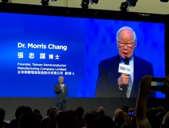
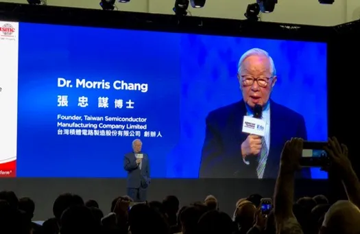
Over the past three decades, most of the world’s innovations have centered largely on business models and involved iterative advances of existing technologies, with none matching the global impact of the top 10 semiconductor industry discoveries and advances, Dr. Morris Chang, founder of TSMC and the IC foundry model, said at SEMICON Taiwan 2018 this week.Few have as clear a perspective on the transformative power of semiconductors as Dr. Chang, founder of TSMC and father of the IC foundry model. Keynoting the IC60 Master Forum celebrating the 60th anniversary of the invention of the integrated circuit (IC), Dr. Chang listed what he considers the 10 key semiconductor industry innovation milestones since 1948:1. Invention of the transistor by Shockley, Bardeen, and Brattain – 19482. Silicon transistor – 19543. Integrated circuit – 19584. Moore’s Law – 19655. MOS technology MOS FET – 1964 Silicon gate – 1967 CMOS – 1970 6. Memory DRAM – 1966 Flash – 1967 7. Outsourced assembly and test (OSAT) – 1960s8. Microprocessor – 19709. VLSI systems design – 1970-1980 IP and design tools – 1980-present 10. Foundry model – 1985 Among the most consequential semiconductor advances may be yet to come, Dr. Chang said, citing innovations including artificial intelligence (AI) and machine learning, new device architectures, Extreme Ultraviolet lithography (EUV), 2.5D/3D packaging, and new materials such as graphene and carbon nanotubes.Dr. Chang argued that because bringing an innovation into production is immensely more expensive than proving a theory in a lab, innovators are not always the ones to implement and benefit from their novel ideas. Today, innovation costs are skyrocketing, driving more consolidation across the supply chain.Michael Droeger is director of marketing at SEMI.
Read More
Storage and memory chipmaker and SEMI China member Tsinghua Unigroup is gearing up to meet burgeoning product demand with huge investments in its manufacturing plants. But the high-tech enterprise under Tsinghua University is eyeing a much bigger prize – growth of the region’s semiconductor industry and the realization of its ambition to become a more prominent force on the global stage.Inspired by the national strategy, the Tsinghua Unigroup’s big spends include USD 24 billion in Wuhan (Yangtze Memory Technologies Co., Ltd.,) USD 30 billion in Chengdu, USD 30 billion in Nanjing and USD 100 billion in Chongqing, said Liu Hongyu, senior vice president of Tsinghua Unigroup, speaking at the SEMI China Equipment and Materials Committee meeting last month.Advanced packaging is another rich vein of opportunity the region is tapping for expansion, said Liu Hongjun, vice president of China Wafer Level CSP Co., Ltd., another SEMI China member attending the event, hosted by NAURA in Beijing. Hongjun sees strong growth for Fan-in, Fan-out, FCBGA, 2.5D and 3DIC, with Fan-out out front. Liang Sheng, administrative commission director at BDA, a business advisory firm supporting high-technology manufacturing in the E-Town economic development zone, pointed to 5G chips and smart, networked electric automobiles as drivers of the next growth phase of Beijing’s integrated circuit (IC) industry.Global tailwinds are lifting China’s semiconductor industry and the region’s hopes, with SEMI and major industry analysts raising their semiconductor industry growth projects for 2018 to between 9 percent and 16 percent. According to SEMI’s latest market report, global semiconductor industry manufacturing equipment revenue reached USD 17 billion in the first quarter of 2018, logging all-time highs after jumping 12 percent from the previous quarter and 30 percent year-over-year. Korea was the top-performing region at USD 6.26 billion, followed by China at USD 2.64 billion.Tighter integration with the rest of the global semiconductor industry is critical to the growth of China’s chip sector, and SEMI China is squarely focused on this assimilation, said SEMI China president Lung Chu. The spearhead of this effort is the SEMI Innovation Investment Platform (SIIP) China, established by SEMI China last year to help grow China’s pool of skilled workers, promote advanced technology, generate industry capital, and expand China’s semiconductor industry while developing stronger connections with chip sectors in other regions. To strengthen ties with other regions, SIIP China will stage a number of innovation and investment forums this year including Chinese Night at SEMICON West (July 10-12) and a SIIP China Forum in Silicon Valley (July 15). In August, representatives from the Korea chip industry will visit counterparts in China (August), and a China delegation will travel to Japan for meetings (October). SIIP China is also strengthening the region’s links with Germany and Israel as SEMI serves as a crucial bridge between China’s semiconductor sector and the global industry.At the invitation of Shanghai authorities and the Ministry of Commerce of the People’s Republic of China, SEMI China in November will join the China International Export Import Exposition in Shanghai, an event that will underscore China’s commitment to the openness and cooperation of its semiconductor industry with the international chip community. As part of the exposition, SEMI will work with the Ministry of Commerce and domestic chip manufacturers to begin development of a special integrated circuit (IC) zone. SEMI China members are welcome to participate.With workforce development no less vital to the future of China’s semiconductor industry, the Equipment Materials Committee offered potential solutions to the industry’s talent gap. Measures included targeting university students and engineers with industry lectures and courses in key cities, campus recruiting, talent training that members said they are willing to help SEMI coordinate and stage and, much like the push to better integrate China with the global semiconductor industry, mobilizing member resources around a campaign to polish the image of the industry to make it more attractive to students and young workers. Members of the SEMI China Equipment Material Committee gathered at NAURA in Beijing in June for a warm and lively discussion about global semiconductor industry cooperation and growing China’s semiconductor sector.Cherry Sun is a marketing manager at SEMI China.
Read More
What’s next for smarter, more connected electronics manufacturing - Part 3 The fast-maturing infrastructure now enabling analysis of exponentially larger data volumes brings the microelectronics industry to an inflection point, where the winning companies will be the first to master the use of this data to solve the industry’s emerging challenges. SEMI expands its coverage of these vital issues with a Smart Manufacturing Pavilion and three days of talks SEMICON West, July 10-12 in San Francisco. While deep learning is starting to be applied to image recognition for wafer inspection, it is also being considered for sequential pattern recognition in order to evaluate equipment parameter traces. The next emerging applications will start to use those learned patterns to predict outcomes, and then use those predictions to automate process control. One early application of deep learning is IC process development. “People don’t think of research and development as the first place to automate, but it’s where applying our digitization and simulation has first had impact,” says David Fried, Coventor vice president of Computational Products. He noted that insertion is easier in the lab than in the fab. Technology at 10nm and beyond is now so complex that companies at the leading edge must use process modeling to understand the effect of process variation on their designs. Learning cycles can now be accelerated during development by simulating 10,000 digital wafers instead of running 25 actual wafers during screening, Fried says. Applying structured analysis and machine learning to the data simplifies optimization across the 500 or more interrelated process steps. Coventor has recently introduced a statistical analysis package that aids the design and analysis of process variation experiments by using large volumes of data from its models. Fried says these models are next being used to accelerate the yield ramp in manufacturing. Digital simulation also could speed development of high-mix, lower value products While digital twins are best known for their use in complex, high value products like jet engines, the simulation technology could also enable the electronic manufacturing services (EMS) sector to reduce the time, cost and risk of developing its high mix of products. “The EMS sector’s use of digital twins will be vital for it to smooth the move of CAD/CAM digital design data for so many different products into manufacturing, and to accelerate validation testing of designs and products by doing more of it in the virtual world,” says Dan Gamota, vice president of Engineering and Technical Services at Jabil. Gamota also highlights the push for traceability from the automotive and healthcare markets, where the digital models could be used to quickly assure that the design was built exactly as specified. “In the past year, traceability has evolved from just ‘nice to have’ to ‘how to achieve,’” he adds. “Companies are expecting it, but aren’t willing to accept the cost and risk of doing it alone. We need the community to discuss realistic implementations, identify the most critical elements and bring together the ecosystem partners to build baseline reference architectures for key digital building blocks. The community also needs to assure the reliable flow of data among the electronic manufacturing segments from semiconductor to OSAT to EMS.” Predictive maintenance and virtual metrology applications could mature in next few years While predictive maintenance initially seemed a likely early application of machine learning in factories, it remains a challenge for the electronics sector. “The difficulty is that it’s not clear where to get the most bang for the buck,” says Tom Ho, president of BISTel America, noting that it may make the most sense to track the failure performance of a single expensive part, like an electrostatic chuck, since predicting the failure performance of a whole complex system like an etcher is much harder. “Collecting enough data from all failure types, including especially the rare events, is difficult unless you have a long history of a lot of tools,” adds Doug Suerich, PEER Group product evangelist. “The gain from collecting performance information from many tools across the industry could be big, but many companies still need to overcome concerns around exposing their IP.” Another big opportunity for prediction is virtual metrology – predicting the wafer outcome from the process or sensor data with enough accuracy to replace the physical metrology. “Virtual metrology is improving, and since metrology can be slow and expensive, any reduction could mean a huge potential savings,” says Suerich. “But it is still seen as too scary for many companies. Two to three years from now, companies will expand the practice from lower risk areas into processes that require more confidence in the results.” Moving beyond prediction to automated control needs digital models Once the results are predicted, the model can be used to control or automatically optimize a process and enable the system to learn by itself, usually by reinforcement learning on a digital model. The model can then independently make adjustments to optimize the manufacturing process. “Automated process development is getting close now. Instead of smart guys turning the knobs, deep learning is automating the smart tuning,” says Suerich, suggesting the industry could see widespread adoption in as little as two to three years. This type of machine learning needs a good digital model, and masses of data for learning. One approach uses human experts to build a physics-based model of the clearly understood parts of the process, then turns to deep machine learning to optimize the lesser-understood variables. The alternative, the data-first approach, runs a computer algorithm to suggest the solution purely from data, without human input, and then relies on the human to evaluate the usefulness of the results. Modeling digital twins of wafers could enable automated process control, chamber matching, and fleet matching, says Fried. If every wafer had its own virtual twin with all the upstream metrology and structural information needed to make equipment control decisions, it could feed forward that information to enable the seamless transition from one step in the process to another based on understanding their complex interrelationships. This could potentially improve uniformity across wafers and equipment, and reduce the need for metrology, he argues. Moving metrology sensors into the chamber will also require model-based algorithms to enable dynamic process control in close to real time, says Fried. These algorithms will be needed to acquire, parse, and process the data at high speed, and then to choose how to adjust the controls. “There will be a model behind collecting and interpreting the metrology data,” he notes. “That’s a really rich vein for improvements in process control.” “The end goal is to collect equipment data in real time, analyze it with AI, and send back controls to optimize manufacturing processes,” Jabil’s Gamota says. “This requires a robust architecture for communication between equipment and consistent formats for data collection and analysis. But the cost and complexity of this heavy lifting is too great for any one company to do alone. We need a consensus-based architecture for ingesting, analyzing and acting on the data.” SEMI tests data transfer protocols, benchmarks best practices SEMI is launching a smart data project to identify the various data transfer protocols needed for inter-company communications. The project will feature a proof-of-concept model in a development fab to produce verifiable results so SEMI can better understand how different approaches meet member needs. SEMI’s smart manufacturing technology communities and the Fab Owners Alliance are also benchmarking current smart manufacturing practices in the microelectronics industry to help SEMI members better understand the path forward and potential return on investment. Speakers over all three days at SEMICON West addressing these issues include Active Layer Parametrics, Applied Materials, Applied Research Photonics, ASML, Bosch Rexroth, Cimetrix, Coventor, ECI Technologies, Edwards Vacuum, Final Phase Systems, GE Digital, Infineon, Jabil, Lam Research, Osaro, Otosense, PEER Group, Qualcomm, Rockwell Automation, Rudolph Technologies, Schneider Electric, Seagate, Siemens, Stanford University, TEL, TIBCO Software. See semiconwest.org. What’s next for smarter, more connected electronics manufacturing - Part 1 What’s next for smarter, more connected electronics manufacturing - Part 2 Paula Doe, SEMI
Read More
The fast-growing automotive semiconductor market means big change for the IC supply chain. Beyond the obvious demands for reliability and traceability, the sector is moving towards simpler and lower-cost solutions while facing the daunting challenge of automating driving in a complex world. The need for simpler and cheaper automotive intelligence will likely drive acquisitions to build complete platform solutions that are easier to integrate. This demand has already spawned a market for pre-configured test cars to save developers time and money, and is driving LiDAR (Light Detection And RADAR) towards lower-cost, solid state solutions. “The growth of the automotive electronics market provides a great opportunity for the IC supply chain to differentiate on specialty processes and quality for the high-volume automotive business with its long design cycles,” says Scott Jones, principal, strategy, at KPMG, who will speak in the automotive program at SEMICON West. “This differentiation is a chance to reduce chip suppliers’ dependence on scaling volume for the mobile phone world with its short-cycle volatility of winning and losing sockets.” He notes that increasing demand for automotive ICs is also reinvigorating the eight-inch supply chain and spurring opportunity for specialty products such as compound semiconductor devices for power efficiency. Supplying the automotive market also means addressing automotive reliability requirements, which can be 10 times more stringent than for consumer devices. At the same time, the industry must sustain fast-paced development cycles required for the volume and diversity of low-cost IoT devices, manage the segmented supply chain for both those markets, and still spread development costs. Another big challenge for the supply chain will be to automate testing and update vast amounts of embedded software in these automotive devices. “The more complete solution a company can put together, the more the automakers will gravitate to it. They want simplicity,” Jones suggests. Smaller players will need to differentiate with IP and acquire other IP provider to build a broader platform, or be acquired and folded into an all-in-one solution.AutonomouStuff helps accelerate and simplify development of autonomous driving solutionsAutonomouStuff is helping to speed development of these platforms. The company has grown from a sensor distributor into a supplier in the emerging niche of vehicles preconfigured with key interfaces for sensors and controls. These interfaces can then be customized by integrating different components for developers to test their applications. AutonomouStuff offers developers a lineup of vehicle models pre-configured with the interfaces needed to add desired chips, sensors and software to develop their autonomous vehicle systems. Source: AutonomouStuff.“Whether they’re major chipmakers or AI software startups, they don’t have a year to build their own vehicle platforms themselves for developing autonomous vehicle systems,” says Wolfgang Juchmann, VP sales and business development at AutonomouStuff. Juchmann, a SEMICON West speaker, will bring a demonstration vehicle to the show. “In four to six weeks we can prepare a custom test car with selected sensors, enabling users to start testing their computer platforms and software. It’s faster and more cost-effective for us to supply the car with the needed interfaces.” He notes that developers are using some 300 AutonomouStuff vehicles in the field. AutonomouStuff customers are starting to transition from testing on a single car or two to testing on mini-fleets with 50 to 100 vehicles. Beyond sensors and pre-configured vehicles, the next step will be to add more data intelligence services to help with capabilities like tagging the data for training, Juchmann says. AutonomouStuff already offers hardware to support Baidu’s Apollo open-source software stack and data set. The company was recently acquired by the Swedish holding company Hexagon to help support expansion.CMOS silicon LiDAR nears automotive qualificationInnovations in the hyper-competitive LiDAR market, where burgeoning demand is driving the race to develop various types of solid-state devices, may also help reduce the cost of autonomous vehicles. Among the roughly 40 LiDAR suppliers, at least one – Quanergy – is taking advantage of 45nm and 32nm foundry CMOS volume production. The company uses voltage through the semiconductor stack to change the refractive index, controlling the phases of optical beams and the resulting interference patterns of light exiting the chip to quickly steer the laser beam without the need for moving parts, much like the phased array radar its team developed earlier. Solid state LiDAR image with object recognition software. Source: QuanergySo far, most of the small LiDAR units have shipped to the security, industrial automation, drone, robots and 3D mapping markets. However, Quanergy CEO Louay Eldada, another SEMICON speaker, says the company is also winning automotive designs and expects automotive shipments to take off early next year, once automotive certification testing is completed. “We can get design wins because standard CMOS production at TSMC makes us a known entity,” says Eldada. To prevent component misalignment, the company produces its own specialized packaging to secure the laser, phase control ASIC, optical phased-array emitter, detector array, and receiver readout ASIC at its plant in Silicon Valley or the facility of its automotive partner Sensata. Through its software business, Quanergy offers an artificial intelligence (AI) perception program for object recognition and LiDAR tracking. The solution uses the people-tracker software the company acquired from Raytheon.SEMICON West this year expands to three full days of automotive electronics programming and features a Smart Transportation Pavilion. Other companies with experts who will speak as part of the program include XPT/NIO, Infineon, McKinsey, Voyage, GM Cruise, Bosch, Deepen AI, Airbus A3, Nvidia, Excelfore, Byton, Macronix, SK Hynix, SAP, Xilinx, Achronics, California Fuel Cell Partnership, Velodyne, Lam Research, KLA-Tencor, SCREEN, Rockwell, Versum Materials, TechSearch International, Entegris, ASE, Amazon, Continental and Wind River. www.semiconwest.orgPaul Doe, SEMI
Read More
SEMI’s mantra is: Connect, Collaborate, Innovate. This mantra has delivered industry-enabling value to our members since SEMI’s beginnings in 1970. It has been essential for SEMI members to grow and prosper locally, while being synchronized globally. As the electronics manufacturing business has become more complex and interdependent, SEMI’s mantra has increasingly been applied across the full span of electronics manufacturing.With the IC industry now worth over $400 billion in annual revenue, developing a single new chip can cost hundreds of millions of dollars. Consequently, industry players now connect, collaborate, and innovate in new, but more often, deeper ways. This is especially true with IC design – what’s possible in chip design is only possible if the manufacturing processes can be developed as projected. It makes sense, as complexity grows and the stakes get higher, that design and manufacturing are closely linked and apply the SEMI mantra together. Where Electronics Begin“Where Electronics Begin” is the tagline of the Electronics System Design Alliance, or the ESD Alliance. It aptly distills the fact that all IC manufacturing begins with design – and the design ecosystem. This week, SEMI announced it reached an agreement with the ESD Alliance to join SEMI as a SEMI Strategic Association Partner. The ESD Alliance will become part of the SEMI organization in 2018. With the ESD Alliance and its community joining SEMI, its membership will complete the full electronics design and manufacturing span.This is a momentous step forward. The ESD Alliance’s ecosystem is vital and thriving and includes the world’s leading EDA and IP companies. Within the ESD Alliance community, Aart de Geus (Synopsys), Wally Rhines (Mentor, a Siemens Company), Simon Segars (Arm), and Lip-Bu Tan (Cadence), among others, are already familiar figures, having brought their thought leadership to SEMI platforms in the past. Now they, and the rest of the ESD Alliance members, will be able to more directly work with semiconductor equipment manufacturers, devices makers, and the rest of SEMI’s membership.At events like SEMICON China, which recently concluded in March and attracted over 90,000 attendees, SEMI and the ESD Alliance members will be able to efficiently connect and engage the supply chain players and find new areas for collaboration. As SEMI’s membership looks out towards new applications and systems opportunities, having both ecosystems together will find possibilities faster and innovate approaches more practically. The ESD Alliance will maintain its distinct community identity and governance while having access to, and the ability to augment, SEMI’s global platforms including seven regional offices, programs and expositions (including SEMICONs), advocacy (including trade, tax, talent, and technology), industry research and statistics, and other SEMI Strategic Association Partner and technology communities.SEMI will gain direct access to the electronics design ecosystems to provide a deeper and wider value – to its combined membership – with SEMI’s mantra. SEMI and its more than 2,000 corporate members and more than 1.2 million stakeholders look forward to connecting, collaborating, and innovating with the ESD Alliance and its members. SEMI’s global reach and wide span of membership with ESD Alliance’s deep expertise in design and IP is truly the best of both worlds for all stakeholders.Connect: Design ManufacturingSEMI’s members have been reaching into the electronics design ecosystem and the ESD Alliance members have been reaching into SEMI’s ecosystem to optimize design and manufacturing process for lowest cost and highest yield. This week’s announcement is a step forward to directly and more intimately connect electronics design and manufacturing for the supply chain to work more closely together in full synchronization. Collaborate: From Beginning to End in Electronics ApplicationsWith the ESD Alliance joining SEMI as a Strategic Association Partner, SEMI members can better collaborate across the full supply chain. Gone are the days when it was enough to collaborate only with one’s direct customer. Today, for example, components and c-subs suppliers frequently collaborate not just with their OEM equipment manufacturer customers, but with device manufacturers – and even system integrators. To be successful, companies are striving for connection to their customers’ customers.The ESD Alliance, with its design ecosystem and linkage to the fabless community, will join three existing SEMI Strategic Association Partners: Fab Owners Alliance (FOA), MEMS Sensors Industry Group (MSIG), and FlexTech (the association representing the flexible hybrid electronics ecosystem). These relationships now cover the entire span of electronics manufacturing.To provide focused collaboration across the full supply chain, SEMI has developed five vertical application platforms: IoT, Smart Manufacturing, Smart Transportation, Smart MedTech, and Smart Data. These have been chosen because of unique and pressing needs to synchronize the supply chain and to engage and develop solutions collectively.Innovate: Faster FutureWith the confluence of emerging digital disruptions and new demand drivers, forecasts suggest the IC industry could grow to over $1 trillion in annual revenue by 2030. To deliver this growth, the supply chain must efficiently innovate together. SEMI’s value proposition is to speed the time to better business results for its members across the global electronics (design and) manufacturing supply chain. The addition of the ESD Alliance as a Strategic Association Partner is a key contributor to deliver this value proposition for the industry to grow and prosper now and in the future.
Read More