downloadGroupGroupnoun_press release_995423_000000 copyGroupnoun_Feed_96767_000000Group 19noun_pictures_1817522_000000Member company iconResource item iconStore item iconGroup 19Group 19noun_Photo_2085192_000000 Copynoun_presentation_2096081_000000Group 19Group Copy 7noun_webinar_692730_000000Path
Skip to main content
Default Banner Image

innovation

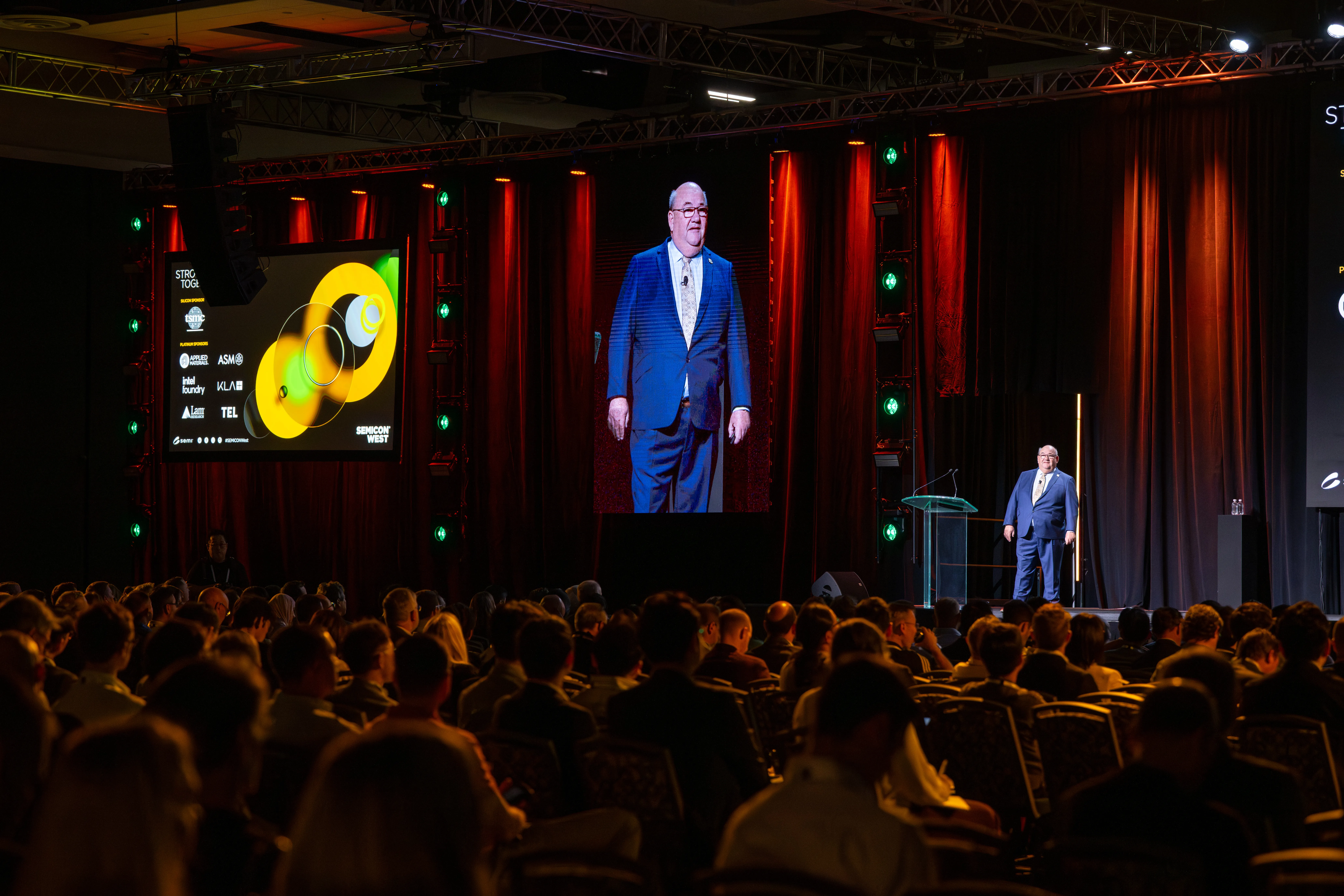
SEMICON West 2025 marked a year of many milestones. Not only was it the first SEMICON West ever to take place outside of San Francisco Bay Area, but it was also its largest exhibition in over 18 years. This year saw a 45% increase in booths, along with a 60% surge in registrations over 2024. The CEO Summit Keynote Series also returned to SEMICON West, featuring 14 unique presentations from October 7-9 at Arizona’s Phoenix Convention Center. Top leaders from both government and industry shared insights on a range of pertinent topics, from technology innovations, to emerging partnerships, sustainability and supply chain initiatives, and more. The keynote series began with opening remarks from SEMI’s President and CEO, Ajit Manocha, who urged audience members to focus on strategies that drive the industry forward and reinforced the importance of collaboration. He also outlined SEMI’s current priorities, including mitigating talent shortages, environmental disruptions, and geopolitical volatility.For those who missed the CEO Summit Keynote Series, this blog offers a summary of each presentation. The State of Arizona“In Arizona, vision becomes opportunity, and opportunity becomes action.” – Katie HobbsSEMICON West’s keynote series kicked off with Arizona Governor, Katie Hobbs, who underscored the expansive growth of Arizona’s semiconductor industry. She highlighted TSMC’s $165 billion investment in Arizona, the largest foreign direct investment in the state’s history, as well as more than 60 other semiconductor expansions that have taken place in the state. There are several reasons, Hobbs said, why Arizona has become an attractive place for semiconductor companies. The local talent base is one, with Arizona ranking among the top five states in the country in this area. Hobbs also highlighted Phoenix’s reliable energy grid, pro-business climate, and 100-year plan for water.AI in Every Layer: Future-Ready Strategies for Technology and Talent“This much disruptive innovation can’t be done by any one company. It requires a broad collaboration ecosystem.” – Sesha Varadarajan Following Hobbs, Sesha Varadarajan from Lam Research discussed AI-related challenges and budding solutions that address them. With AI setting the pace of industry innovation, Varadarajan emphasized the need for clarity for device-specific roadmaps. For example, logic is transitioning from FinFET to Gate-All-Around, DRAM is moving toward 3D architectures, and advanced packaging innovations are enabling continued scaling. Ultimately, Varadarajan concluded that device roadmaps would come down to three things: thinner materials, taller structures, and smaller features. Lastly, he noted that workforce development training often lags behind industry demand, highlighting Lam Research’s Semiverse education platform as a solution. Stronger Together - Building a Resilient Future for Semiconductors“When you’re working at an atomic level of precision, every detail matters.” – Jon KempDupont’s Jon Kemp offered insight into how the semiconductor industry can usher in a new wave of transformation. To achieve this, he highlighted three strategic priorities: supply chain, sustainability, and AI. Kemp emphasized bringing manufacturing closer to customers, designing products for energy efficiency, and creating new AI architectures that address mounting performance expectations. He also announced that Qnity, an integrated material solutions provider, will be spinning out of DuPont on November 1, 2025. Where Vision Meets Execution: Global Executive Summit (GES) Unites Industry Leaders“[There has been] lots of progress so far, and we want to build on that momentum.” – Carolin Seward. Carolin Seward from Google took the stage to discuss the upcoming Global Executive Summit (GES) from December 15-16 in Tokyo. This invitation-only meeting will convene industry executives to discuss core sustainability issues, like advancing abatement, pursuing gas substitution, driving green materials, and enabling low-carbon energy. Closer to Home: Costa Rica as a Partner for Successful Operations in the Western Hemisphere“Costa Rica is ready to become part of the solution.” – Manuel Tovar RiveraManuel Tovar Rivera discussed Costa Rica’s efforts to bolster its semiconductor industry. With its close proximity to the U.S., three decades of advanced manufacturing experience, and free trade, Rivera also explained the benefits of U.S. and Costa Rica collaborations. To meet the needs of its trade partners, Costa Rica is developing its local talent base, attracting foreign professionals, offering incentives for R D and startup investment, and streamlining its regulatory processes. Advancing 3DIC Technologies to Propel AI Innovations“Our best day is still ahead of us.” – Jun HeClosing out the Tuesday keynote series was TSMC’s Jun He, who spoke about the packaging innovations that are pushing the world closer to more advanced AI. The key benefit of advanced packaging, he said, is to enhance AI performance and efficiency–but excellent yield is a nonnegotiable requirement. He underscored the growing importance of CoWoS, or Chip-on-Wafer-on-Substrate packaging structures, as well as fluxless thermocompression bonding, to help meet demand for AI. AI Supercomputing for Next Generation Semiconductor Design and Manufacturing“AI factories transform electricity into intelligence.” – Timothy CostaNIVIDA’s Timothy Costa began the Wednesday keynote series by highlighting physical AI as “the next trillion-dollar industry,” and outlined how the company is helping the industry get closer to that benchmark. Costa noted the three NVIDIA computers being used to train physical AI models – Omniverse for simulation, DGX for training, and Jetson AGX for deployment. All of these, he said, need to work together to deliver on physical AI promises, like robotics, autonomous vehicles, and others. Executive Panel – Powering the Next Decade: AI’s Impact on Semiconductor Infrastructure and Market“We’re living in the most exciting time in the world of computing.” – Mukesh KhareFollowing Costa, the CEO Summit Keynote stage transitioned into a panel discussion with industry-leading AI experts – including Laura Matz from Merck KGaA, Darmstadt, Germany, Mukesh Khare from IBM Research, Mark Dougherty from TEL, and Angada Sachid from ASM. The panel was moderated by David Anderson, President of NY CREATES. Although there was much said during this 50-minute panel, a few key points were emphasized. First, Khare highlighted open chip design activities for AI models as a way to alleviate cost burdens. Design costs for more advanced nodes, he said, can be greater than $500 million. Matz also outlined the urgent need to develop PFAS-free materials without sacrificing yield. Currently, there are several areas where the industry doesn’t have a solution for PFAS, but AI models may be able to help.Sachid also mentioned power challenges, pointing to how one or two misplaced atoms can be the difference between a power-efficient versus a power-hungry chip. Deposition needs to be perfect at 10 trillion separate locations, and he pointed to AI as an emerging solution for this as well. However, despite the promises of AI, the panelists underscored that people are still a company’s most valuable asset. Revolutionizing Semiconductor Collaboration: The Emergence of AI-Driven Industry Platforms“You can make better decisions with more information.” – John KibarianWhile nearly every session touched on the need for industry-wide collaboration, John Kibarian from PDF Solutions focused on making this feasible. In today’s highly complex semiconductor supply chain, every point is critical, from fabless companies, to foundries, OSATs, and external vendors. To make industry-wide collaboration practical without compromising IP, he noted the importance of secure infrastructure, automated orchestration, and robust AI agents to assess and analyze the raw data that often goes unused. Kibarian highlighted PDF Solutions’ secureWISE system as a tool that’s already in place to address these needs. Shaping the Future of Semiconductors in the U.S.“The specific things that drove growth were the evolution of new applications.” – Giel RuttenAs the semiconductor industry continues its journey to $1 trillion in annual industry revenue, Amkor’s Giel Rutten provided an update on the U.S. market. Because OSATs are heavily concentrated in Asia, this poses a significant challenge for reshoring U.S. manufacturing. Most OEMs, he said, are looking to OSATs to handle several of their processes because it’s cheaper than doing it themselves. Rutten detailed the mounting complexities of backend assembly, including rising demand for multiple, high-bandwidth memory stacks that traditional SoCs can’t accommodate. This is pushing the industry toward heterogeneous integration, which further complicates the supply chain. Rutten concluded by emphasizing the importance of industry-wide collaboration, and noted that Amkor’s Arizona fab will offer a complete, turnkey supply chain in the U.S. Fireside Chat – Harnessing Digital Transformation to Empower People and Accelerate Precision“The more we double down on technology, the more we should also elevate humanity and double down on our values.” – Khadija Ben HammadaWith a strong emphasis on AI during the 2025 keynote series, the final discussion on Wednesday brought humans back into the spotlight. Khadija Ben Hammada from Merck KGaA, Darmstadt, Germany and Daniel Drellich from EMD Electronics (the electronics business of Merck KGaA, Darmstadt, Germany), joined Jon Krohn on stage for an insightful talk on empowering employees in today’s AI era. Of the many things discussed, both Hammada and Drellich underscored the need to build trust with employees, as many of them fear being left behind by the technology. While it’s true that companies have invested heavily in AI, such investments also require them to educate teams on how to use it. This can best be achieved through a culture, they said, where people feel comfortable enough to learn in the first place. The panelists also highlighted the importance of finding the right AI tools for specific purposes, instead of blindly choosing the most sophisticated solution. Partnering to Serve the Demands of the AI Era“A foundry business is a trust business.” – Kevin O’BuckleyAlthough there’s no shortage of discussion about the industry’s road to $1 trillion, Intel’s Kevin O’Buckley shared where that trillion-dollar value is being realized. Based on recent projections, the simple breakdown he presented shows that 50% is generated by fabless companies, 25% by suppliers, and 25% by foundries and OSATs. With the rise of fabless companies, he highlighted the need for foundries to provide value to customers, including better power delivery solutions and predictable execution on customer projects. He also shared Intel’s efforts, like bringing its 18A node into production, its PowerVia for backside power delivery, and new slurry formulations for delicate wafers. Bridging the Talent Gap: Accelerating Workforce Solutions for Semiconductors“We're building opportunity and innovation into the semiconductor workforce.” – Shari LissShari Liss, VP of Global Workforce Development and Initiatives at SEMI, detailed the current state of the industry’s workforce needs. More than 170,000 new workers, she said, will be needed in the U.S. in the next five years. To help close the talent gap, Liss shared a roadmap of the SEMI Foundation’s efforts, ranging from awareness programs that target children as young as seven, to apprenticeship programs for adults. So far, the SEMI Foundation has reached 1.25 million students through its apprenticeship and certification programs, 3,300 people through its expanded childcare access, and 7,000 people through its SEMI U courses. Liss also highlighted the SEMI Foundation’s operator role in the newly established National Network of Microelectronics Education (NNME) — a national program that aims to build regional centers around the U.S. for microelectronics education and training. Requests for proposals are now open, and applications are due in December. American Chip Revival and the Trusted Tech Imperative“Trust is the most important word in any language.” – Keith KrachThe 2025 keynotes series concluded with Purdue University’s Keith Krach and former undersecretary of state. During his time as undersecretary, he emphasized the importance of building trust to rebuild the U.S. semiconductor supply chain. Through his trust-first approach, Krach helped secure TSMC’s presence in Arizona, leading to better jobs and a stronger domestic chip ecosystem. In addition, he was instrumental in creating a clean 5G network that later became the xGTT, or the Global Trusted Tech Standard. SEMI would like to thank all speakers, sponsors, and attendees for the success of this year’s CEO Summit Keynote Series. Joe Stockunas is President, SEMI Americas.
Read More
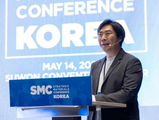
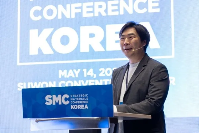
Driven by the recovery of the overall semiconductor market and rising demand for advanced materials for high-performance computing (HPC) and high-bandwidth memory (HBM) manufacturing, global semiconductor materials revenue rose 3.8% year-over-year in 2024. At the heart of this momentum, Strategic Materials Conference (SMC) Korea 2025 brought together approximately 300 industry leaders on May 14 to discuss bold innovation roadmaps and the evolving challenges of the new AI-driven era.Celebrating its 10th edition, SMC Korea served as a convergence point for leaders across the semiconductor ecosystem—including materials suppliers, equipment manufacturers, chipmakers, and academia.“This year’s SMC Korea has recorded the highest level of Q A engagement. A full hour was dedicated solely to an audience-driven panel discussion, where questions ranged from materials technology and business to semiconductor process roadmaps and market outlook. The depth and interactivity of the dialogue reflected the standards of leading technical conferences. Some attendees even noted that it surpassed any academic or industry symposium currently held in Korea,” said Oh Kim, Co-chair of the EMG Korea Chapter and representative of Air Liquide Solutions Korea.Exploring Next-Gen Technologies: 3D DRAM and CFETThe first session focused on next-generation semiconductor technologies, highlighting the future of materials and processes for 3D DRAM and Complementary FET (CFET) devices.Dr. SukKoo Hong, Head of the Material Development team at Samsung Electronics, kicked off the session by outlining a roadmap for materials innovation in 3D DRAM and CFET. Dr. Hong emphasized key technical challenges in the development of 3D DRAM and CFET, highlighting the need for continued innovation in process integration and material engineering. Building on this, Dr. Hong stressed the increasing complexity of material processes and the critical need for tight cross-industry collaboration.Dr. Inhee Lee, Director of imec’s Active Memory Program, highlighted the diminishing improvements in DRAM scaling and emphasized the urgent need for new high-k materials to enable higher density in next-generation 3D DRAM and 4F² DRAM architectures. Dr. Lee emphasized the need for further validation on performance shifts and data retention time resulting from changes in channel materials and architectures.Professor Changhwan Choi of Hanyang University presented key material and process trends for CFET devices, focusing on monolithic and sequential integration as well as Backside Power Delivery Network BSPDN) technologies.The session also featured a presentation by Linghzhi Zhang, Director of Product Management at Air Liquide Advanced Materials focused on “Si, Ge, B Hydrides for Next Generation Semiconductor Devices – Challenges and Perspectives.”The Future of Semiconductor Materials: Market Trends and Innovation StrategiesThe second session highlighted semiconductor materials from multiple perspectives, including market outlooks, advanced technology solutions, and strategic responses to industry challenges.Dr. Prayudi Lianto, Technology Manager at Applied Materials, discussed the technical barriers currently facing HBM, particularly the stacking height limitations. Dr. Lianto highlighted the importance of advanced packaging technologies such as through-silicon via (TSV) and hybrid bonding, and emphasized the critical role of material innovations. Key challenges include void formation during TSV gapfill and developing robust bonding strength and interfacial metals for low-temperature hybrid bonding.Andy Tuan of Linx Consulting provided a market outlook centered on macroeconomic shifts and evolving supply chain structures. Tuan noted that while the semiconductor industry is undergoing a short-term correction, the materials market continues to grow steadily—driven by 300mm logic, DRAM, and 3D NAND. Tuan projected that demand for process materials such as lithography, deposition, and CMP will see a notable recovery post-2025.Dr. Deoksin Kil, Senior Fellow at SK hynix, underscored the growing significance of advanced process materials—including high-performance photoresists, functional chemicals, and CMP slurries—as enablers of semiconductor scaling and 3D evolution. Dr. Kil also stressed the need to maintain consistent quality and supply chain resilience, while pursuing sustainability through low-GWP gases and PFAS-free materials.The session also featured the following presentations:Yohan Ahn, Senior Director, Entegris: “Technological Trends and Necessity of Material Contamination and Filtration for Wafer Defectivity Control in HBM Manufacturing”Dr. Mikko Utriainen, Chipmetrics: “Advancing ALD Tool Qualification Using Ultra-High-Aspect-Ratio Test Structures”SEMI Korea extends its gratitude to all SMC Korea 2025 sponsors for making this insightful conference possible. Dongwoo Fine-chemJSR Electronic Materials KoreaHuntsman Performance ProductsUP ChemicalDuPont Electronics IndustrialDongjin SemichemSK trichemTEMCEntegrisAir Liquide Solutions KoreaJaegwan Shim is Senior Specialist, Marketing at SEMI.
Read More
As the demand for more powerful and efficient chips continues to grow, and the pace of semiconductor manufacturing in Arizona rapidly expands, so does the need for a highly skilled workforce capable of meeting these challenges. The SEMI Foundation’s SEMI Career and Apprenticeship Network (SCAN) Arizona Team is committed to building a robust workforce pipeline through strategic partnerships and initiatives that connect industry to education. These initiatives include fostering science, technology, engineering, and math (STEM) enthusiasm in K-12 (kindergarten through high school) classrooms to creating earn-and-learn opportunities through apprenticeships and collaborations with leading semiconductor companies. The Foundation’s Arizona team has coordinated key events and initiatives in the state that showcase a holistic approach to addressing workforce challenges, many of which could be expanded and replicated throughout the US and even globally.Arizona SciTech STEM and Innovation Summit: Fostering STEM Enthusiasm The Arizona SciTech STEM and Innovation Summit has long been a hub of innovation, offering students, educators, and the community an immersive experience in STEM. This year’s summit was no exception. Showcasing hands-on activities, workshops, and demonstrations, the event connected STEM industries with Arizona's next generation of talent.The SEMI Foundation Arizona team led activities and sessions demonstrating the Foundation’s work with educators and workforce experts to explore how semiconductor curricula can be integrated into classrooms. Through engaging workshops featuring SEMI Foundation High Tech U Micro:bit STEM kits and Baltu Technologies, and a panel discussion with educators talking about the importance of industry in the classroom, participants explored exciting careers and how to introduce industry opportunities to students. These interactions emphasized the real-world applications of classroom learning, showing the path to careers in high-tech industries.Teachers students participate in a hands-on Micro:bit STEM Kits workshop during AZ SciTech STEM and Innovation Summit held on October 22, 2024. Panelists discuss the future of the semiconductor industry incorporated into students’ education. From left to right: Dee Pinkston (Chicanos por la Causa), Raquel Diaz (Trevor G. Browne High school), Rachna Mathur (ASU prep, ASU, STEMology), Kenneth Mims (Science Prep Academy Neurodiversity Education Research Center). Apprenticeship 101: A Guide to Workforce ReadinessIn a landscape where technical skills are increasingly critical, the Apprenticeship 101 workshop provided a crucial introduction to the benefits of how earn-and-learn programs are transforming careers in semiconductors and beyond. Hosted by: Arizona Commerce AuthorityArizona@Work SEMI Foundation Federal/State Apprenticeship Developer Scott EllsworthSEMI Foundation SCAN Arizona team The City of Phoenix This event gave attendees an overview of apprenticeship opportunities in fields like semiconductors and advanced manufacturing.Participants learned how these programs build bridges between education and employment, offering both practical experience and a clear path to career advancement. A notable highlight was the emphasis on underrepresented groups, showcasing how apprenticeships can empower individuals to succeed in high-demand fields.Panelists highlighting pathways to careers in semiconductors with a focus on earn-and-learn opportunities. From left to right: Nick Irigoyen (SEMI Foundation), Michael Rosas (Arizona Commerce Authority), Scott Ellsworth (SEMI Foundation), Joan Bueno (Arizona Apprenticeship Office), James A. Montoya (ARIZONA@WORK), Stephanie Varela (City of Phoenix) Apprenticeship 101 Panelists. From Left to Right: Nick Irigoyen (SEMI Foundation), Scott Ellsworth (SEMI Foundation), Joan Bueno (Arizona Apprenticeship Office), Stephanie Varela (City of Phoenix), Perla DeBaggis (SEMI Foundation), James A. Montoya (ARIZONA@WORK) Intel Apprenticeship Program Support: A Step Toward Workforce Expansion Intel’s apprenticeship announcement signaled a transformative step for Arizona’s tech industry. With a focus on diversity and inclusion, Intel’s initiative aims to recruit participants from all backgrounds, ensuring a broad and equitable talent pool. Their current cohort of apprenticeships started with 9 women from the Fresh Start Foundation. The team worked with Arizona@Work representative Stephanie Varela to provide the apprentices with an overview session of the workforce innovation and opportunity act resources available to them. These kinds of resources provide alignment and improvement of employment, training, and education programs to promote individual growth. By investing in the workforce of tomorrow, Intel underscored its commitment to Arizona’s economic growth and technological leadership.Intel apprentices Gabriella Medina and Laura Jabalera are paving the way for women in the industry. Learn more about their inspiring journey here. TSMC Apprenticeship Announcement: Driving Innovation and InclusionSimilarly, TSMC’s apprenticeship program launched on November 19, 2024, bringing excitement and opportunity to the state. The program offers specialized training for individuals seeking careers in semiconductor manufacturing, a vital industry for Arizona’s economy.TSMC’s announcement emphasized collaboration with educational institutions, including community colleges and universities, to ensure apprentices receive both technical training and academic support. TSMC Arizona is investing more than $5 million in this program representing on-the-job training hours and education tuition support for its apprentice employees.The SEMI Foundation SCAN Arizona team joins TSMC apprentices on November 19, 2024 to celebrate the launch of TSMC's groundbreaking apprenticeship programs. Trevor G. Browne High School AET Assembly: Inspiring Young InnovatorsAt Trevor G. Browne High School, the Advanced Engineering and Technology (AET) Assembly served as a rallying point for students interested in high-tech careers. The SEMI Foundation Arizona Team joined their assembly to celebrate the potential of Arizona’s youth, sharing stories of innovation and success in the semiconductor sector.Students gained valuable insights into the industry’s evolving landscape, learning about the impact semiconductors have in cutting-edge technologies and career pathways in engineering and manufacturing. The assembly highlighted the importance of programs like SCAN-AZ and other local initiatives happening in 2025, which aim to bridge the gap between classroom learning and real-world opportunities.Micro:bit Competition: Sparking Innovation in Arizona's ClassroomsThe launch of SEMI Foundation - Arizona’s first Micro:bit Competition is bringing creativity and technology together in K-12 classrooms statewide! Designed to inspire innovation, this competition challenges students to use Micro:bit to develop projects that showcase their technical skills and imagination.From robotics to sustainability solutions, students are exploring real-world applications of STEM through hands-on projects. With categories like Innovation in Education and Creative Arts, the competition encourages participants to think outside the box. This initiative not only highlights the SEMI Foundation’s commitment to STEM education but also fosters the next generation of problem solvers and innovators. The Micro:bit Competition is more than just a contest—it’s a stepping stone for students to explore their potential in high-tech industries.Stay tuned as we celebrate the incredible projects and the bright young minds behind them!ASU Preparatory South Elementary, Grades 3-6 Teacher Michael Grant (Left) receiving his Micro:bit STEM kits for his participating classroom from Perla DeBaggis SEMI Foundation (Right)The SEMI Foundation’s efforts in Arizona exemplify the power of strategic partnerships and innovative programs to build a stronger, more diverse pipeline for the semiconductor workforce. By engaging educators, students, and industry leaders, we are creating pathways that connect education to employment, fostering a future-ready workforce. These initiatives serve as a blueprint for workforce development that can be adapted and scaled nationwide, empowering communities to thrive in the evolving high-tech economy. The SEMI Foundation is thrilled to continue this momentum and expand our impact even further in 2025! Co-Author Perla DeBaggis is the Senior Specialist for Career and Industry Awareness at the SEMI Foundation, focusing on bridging the gap between education and industry. Co-Author Nick Irigoyen is the Project Manager for Project Manager, Workforce Development Apprenticeships at the SEMI Foundation, focusing on initiatives aimed at strengthening the semiconductor talent pipeline in Arizona.
Read More
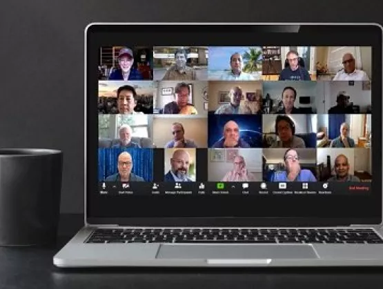
Tracking and quickly diagnosing COVID-19 infections, working from home and telemedicine recently came into sharp focus as technology executives and other subject matter experts from microelectronics heavyweights recently gathered for the first-ever virtual SEMI CTO Forum to explore how the microelectronics industry and their own companies can leverage future technology trends to drive growth. Themed Intelligent Medtech and Wearable Technologies, the forum drew CTOs from ARM, Babblelabs, Brewer Science, Dell, Dow/Dupont, E-Ink, Hewlett Packard Enterprise, Intel, Lam Research, KLA, Microchip, ON Semiconductor, Qualcomm, Tokyo Electron, Ulvac, Veeco and Xilinx. The event is designed as a strategic driver of pre-competitive innovation. Following are key takeaways from the forum. Microfluidics Promises to Speed COVID-19 Diagnosis More than 240 companies worldwide are developing microfluidics solutions to improve diagnosis and treatment of COVID-19 and other conditions, said forum speaker Dr. Kurt Petersen, a member of Band of Angels, Silicon Valley's oldest angel investment group, with an illustrious background1 in technology. And their innovations are bearing fruit. Cepheid, a company founded by Dr. Petersen, has developed a disposable microfluidic cartridge, Xpert Xpress SARS-CoV-2, used by doctors to swab the inside of a patient’s mouth. Highlighting the vital role of MEMS in medical electronics, the tiny powerful devices are behind a test that can detect COVID-19 infection in under 40 minutes. Dr. Petersen also cited a few examples of implantables and injectables under development, including: In vivo chemical sensing: Profusa developed a continuous glucose monitoring sensor via an optical patch. Glaucoma pressure monitors: Injectsense built a silicon chip the size of a grain of rice that is embedded in the eye to measure eye pressure. Retinal implants: Second Sight implanted a 60-electrode array chip that projects images onto the retina to improve vision. Microelectronics Takes Aim at Battling COVID-19 The event’s CTO roundtable, a platform for discussing societal and technology issues, revealed microelectronics technology will likely give rise to solutions for combatting pandemics and new business opportunities both in the short and long run. Areas of the greatest interest included: Tracking and Security: Infection tracking accuracy is key to limiting the spread of viruses yet comes with inherent privacy and security challenges. The consensus view of the executives was that developing trusted hardware capabilities is critical for adoption of accurate infection-tracking technologies. Remote Operation: Executives expect working from home or the use of telehealth to continue building momentum long after pandemic. To give staying power to the remote communications at the heart of these trends, microelectronics ecosystems will need to boost compute performance, both at the edge and in the cloud, while increasing bandwidth to enable applications such as augmented reality/virtual reality (AR/VR), artificial intelligence (AI), machine learning and advanced data analytics. Edge intelligence: The challenge of remote communications spans both people and the Internet of Things (IoT). Questions persist about how hundreds of billions of sensors will connect to the cloud and how much power they will consume. The need to push computing to where data is generated – at the edge – is rising and the necessary underlying technologies will only come by combining various forms of distributed computing and analytics. The microelectronics industry’s ability to seize these opportunities will only be possible with huge strides in innovation, raising concerns among the CTOs about the financial viability of cutting-edge devices because of increasing device complexity and R D costs. Technology partnerships and collaborations – an area where SEMI is contributing and will continue to expand its efforts as it works with the CTO community – will be critical to containing R D costs. SEMI will help the executives identify and mobilize the resources key to future innovation. Improving Home, Work Productivity and Experiences Key to AR Adoption Smart wearables also offer great promise. In just over a decade, AR and VR have grown from science fiction to practical uses such as AR applications for smart contact lenses, said Dr. Mike Wiemer, Co-Founder and CTO of Mojo Vision2. Dr. Wiemer said that while many AR applications remain under development, the technology will only see widespread adoption once it starts to improve productivity and efficiency at home and work and the quality of other experiences. The smart augmented reality contact lens developed by Mojo Vision is a step in that direction. The product’s built-in display gives users timely information about everything they see while remaining invisible by packing 70,000 pixels into a space smaller than a half a millimeter across, making it the smallest and densest dynamic display ever made. The contact lens is powered by an ARM-based processor, with later versions adding an image sensor, eye-tracking sensors and a communications chip. SEMI thanks EMD Performance Materials and Telit for sponsoring the CTO Forum. For more information on the CTO Forum and SEMI’s Smart Data-AI initiative, please sign up on our webpage. 1 Dr. Kurt Petersen is a member of the National Academy of Engineering, an IEEE Medal of Honor winner, and a Life Fellow of the IEEE for his contributions to the commercialization of MEMS technology. 2 Dr. Wiemer also co-founded Solar Junction, where he led technical teams to two world records in solar cell efficiency (43.5% and 44%). He also has patents and papers in Semiconductor Devices Applications, Silicon Photonics, Materials Integration, Lasers, Solar Cells, Solar Systems, and Analog Circuits. Tom Salmon is Vice President of Collaborative Technology Platforms at SEMI. Pushkar P. Apte, Ph.D., is Strategic Technology Advisor for the Smart Data AI Initiative at SEMI.
Read More
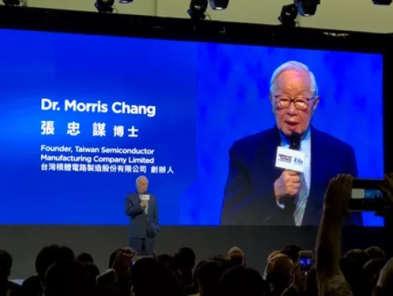
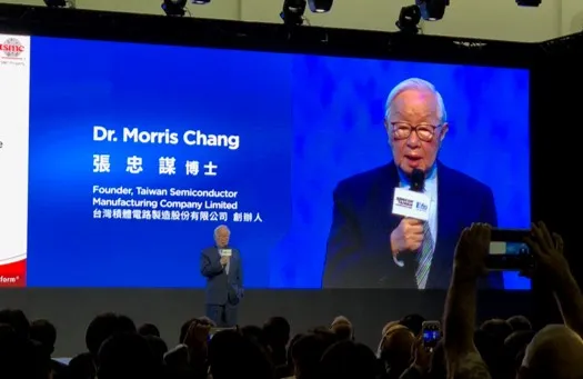
Over the past three decades, most of the world’s innovations have centered largely on business models and involved iterative advances of existing technologies, with none matching the global impact of the top 10 semiconductor industry discoveries and advances, Dr. Morris Chang, founder of TSMC and the IC foundry model, said at SEMICON Taiwan 2018 this week.Few have as clear a perspective on the transformative power of semiconductors as Dr. Chang, founder of TSMC and father of the IC foundry model. Keynoting the IC60 Master Forum celebrating the 60th anniversary of the invention of the integrated circuit (IC), Dr. Chang listed what he considers the 10 key semiconductor industry innovation milestones since 1948:1. Invention of the transistor by Shockley, Bardeen, and Brattain – 19482. Silicon transistor – 19543. Integrated circuit – 19584. Moore’s Law – 19655. MOS technology MOS FET – 1964 Silicon gate – 1967 CMOS – 1970 6. Memory DRAM – 1966 Flash – 1967 7. Outsourced assembly and test (OSAT) – 1960s8. Microprocessor – 19709. VLSI systems design – 1970-1980 IP and design tools – 1980-present 10. Foundry model – 1985 Among the most consequential semiconductor advances may be yet to come, Dr. Chang said, citing innovations including artificial intelligence (AI) and machine learning, new device architectures, Extreme Ultraviolet lithography (EUV), 2.5D/3D packaging, and new materials such as graphene and carbon nanotubes.Dr. Chang argued that because bringing an innovation into production is immensely more expensive than proving a theory in a lab, innovators are not always the ones to implement and benefit from their novel ideas. Today, innovation costs are skyrocketing, driving more consolidation across the supply chain.Michael Droeger is director of marketing at SEMI.
Read More