downloadGroupGroupnoun_press release_995423_000000 copyGroupnoun_Feed_96767_000000Group 19noun_pictures_1817522_000000Member company iconResource item iconStore item iconGroup 19Group 19noun_Photo_2085192_000000 Copynoun_presentation_2096081_000000Group 19Group Copy 7noun_webinar_692730_000000Path
Skip to main content
Default Banner Image

Europe

On April 21, 2021, the European Commission put forward the long-awaited Proposal for a Regulation on a European approach for Artificial Intelligence, introducing for the first time harmonized rules for the development, placement and use of secure and ethical artificial intelligence (AI) in Europe. The proposed regulation’s wide scope subjects providers, importers, distributors, and users of AI systems to regulatory scrutiny. It also includes providers and users outside of the European Union (EU) that deploy AI systems or use AI system outputs in the EU. With extraterritorial scope, the proposed regulation aims to further strengthen the EU’s leadership in shaping global standards and norms for new technologies. A European Path to Safe AI Following a risk-based approach, the proposed regulation classifies AI systems according to the level of danger they pose in the following categories: Unacceptable risk: AI poses unacceptable risk to systems or applications with the potential to manipulate human behavior and exploit vulnerabilities of groups of people to cause psychological or physical harm. Examples of prohibited AI systems include social-scoring systems and biometric identification that can be used by public authorities. High risk: The proposal identifies two main categories: AI systems used as safety components of products (or are a product themselves), and other stand-alone AI systems that have fundamental rights implications. Considering their intended purpose, the proposal identifies specific conformity assessment measures for both groups. AI systems intended to be used as security components will require a conformity assessment by an independent third party. Such systems will also be subject to the same ex-ante and ex-post compliance and enforcement mechanisms as products of which they are part. In contrast, stand-alone AI systems assessed through internal checks would require ex-ante compliance with all requirements of the regulation as well as with robust standards for quality and risk management and post-market monitoring. The proposed regulation identifies eight areas of high risk including AI systems in safety components of products (e.g., machinery, radio equipment, AI applications in robot-assisted surgery), critical infrastructures (e.g., transport), educational and vocational training (e.g., exam scoring) and employment (e.g., monitoring or evaluation of persons in work-related contractual relationships). Prior to their introduction to market, high-risk AI systems will be a subject to strict requirements including the use of high-quality datasets; adequate risk assessment and mitigation systems; high levels of robustness, accuracy, and security; clear and adequate user information; detailed system documentation and logging of activities to ensure traceability of results. Human oversight and control must be ensured. Low and Minimal risk: For limited-risk AI systems (e.g., chatbots), the regulation proposes only minimum transparency obligations, while minimal risk AI systems posing little to no risk (e.g., AI in spam filters) will not be regulated. Boosting AI Excellence from Lab to Market Continuous innovation of AI requires a secure environment that can support responsible validation of AI technologies. To that end, the proposal encourages the set-up of testing and experimentation facilities or so called AI regulatory sandboxes. Established by one or more Member States, the sandboxes will provide a controlled environment to test innovative technologies under strict oversight before their market introduction. These facilities could play an instrumental role in connecting the Europe’s R D ecosystem, creating new partnerships among numerous stakeholders. In addition to regulatory sandboxes, the European Commission intents to set up: A Public-Private Partnership (PPP) on AI, data and robotics designed to implement and invest in strategic research innovation and a deployment agenda for Europe Additional Networks of AI Excellence Centers to foster exchange of knowledge and advance collaboration with the industry Testing and experimentation facilities to test state-of-the-art technology Digital Innovation Hubs, one-stop shops to provide access to technical expertise and experimentation An AI-on-demand platform as a central European toolbox of AI resources (e.g., expertise, algorithms, software frameworks and development tools). Next Steps The proposed regulation is the at the start of a lengthy legislative process and will be debated by the European Parliament and European Council in the coming months. Given the importance of AI, and number of stakeholders involved, it is likely the proposed regulation will face various changes before being applied across the EU. For its part, SEMI Europe will maintain discourse with key public and private stakeholders on the proposed regulation, closely monitoring related policy developments as they unfold. Marek Kysela is senior coordinator of Advocacy at SEMI Europe.
Read More
As the global economy is constantly transformed, the need for new skills has never been higher. The microelectronics industry is thoroughly affected by this urgent need. To develop a workforce fit for the future, it is crucial to invest not only in reskilling and upskilling, but also in skills anticipation and inclusivity. To tackle this need, the European microelectronics ecosystem has adopted many bottom-up initiatives and good practices supporting lifelong learning. Many companies collaborate with universities and training institutes to offer work-based training, and numerous events take place to support women participation in STEM and to attract more young talent to a microelectronics career. Despite these great efforts, further pooling of investments is necessary if Europe is to develop efficient lifelong learning programs. Creating strong skills partnerships is vital for sustainable upskilling and reskilling initiatives. According to the World Economic Forum (2021), greater private-public collaboration on large-scale upskilling and reskilling initiatives could boost global GDP by $6.5 trillion and lead to the creation of 5.3 million net new jobs by 2030. What is the Skills Partnership? Against this backdrop, SEMI Europe is launching the Skills Partnership for Microelectronics. The partnership brings together industrial and education partners from the microelectronics ecosystem to implement the Pact for Skills, an EU initiative which aims to boost upskilling and reskilling investments in key ecosystems for Europe’s competitiveness. Following the high-level roundtable with SEMI Europe’s Advisory Board, hosted by European Commissioners Thierry Breton and Nicolas Schmit, the microelectronics sector was selected in November 2020 as one of the key ecosystems for the first wave of implementation of the Pact, alongside automotive and aerospace/defense. Read more details about the October 2020 roundtable. 59 partners have already endorsed the Pact for Skills for Microelectronics. The Skills Partnership for Microelectronics aims to: Exchange good practices of upskilling and reskilling initiatives of the microelectronics industry Develop sustainable collaboration mechanisms that will monitor microelectronics skill needs, learning from the examples of the METIS blueprint project Promote the microelectronics sector as a career choice Boost the presence of women and other under-represented groups in the sector. The partners will have the opportunity to liaise not only with European, but also with national and regional authorities and clusters, so that a pan-European holistic approach to microelectronics skills development is achieved, and a significant flux of public and private investments on skills is mobilized. To launch this ambitious partnership, SEMI Europe held an initial workshop on March 17. Participants included representatives from the European Commission’s DG Connect, DG Employment and DG Grow, national and regional authorities, and over 70 industry and education partners. The workshop opened with representatives from the European Commission informing all stakeholders about the Pact for Skills initiative, as well as about EU skills-related funding opportunities. In the framework of the Pact for Skills, the Commission will support the ecosystems with a Networking Hub, a Knowledge Hub and a Guidance Resources Hub. These platforms will be available later in 2021 and will act as a one-stop-shop to support the partners and provide information on EU policies and funding opportunities. Other presentations went on to set the scene, presenting the main priorities of the partnership. Françoise Chombar, CEO of Melexis, highlighted the skills challenge experienced by the microelectronics industry. She emphasized the importance of lifelong learning and the danger of the gender disbalance in the sector and underlined the huge innovation potential and profitability that could be unleashed for Europe if the gender gap is successfully addressed. Moreover, the preliminary results of the METIS Microelectronics Skills Strategy were presented, to offer the basis for the partnership’s approach to skills anticipation. The partnership will establish working groups that will investigate the industry needs, leading to a better connection with the offer of education and training programs. Last but not least, the partnership aims to promote national and regional funding of upskilling and reskilling initiatives. In this regard, representatives from national and regional authorities and clusters participated in the meeting. The government of the Basque region had an active role, presenting the region’s priorities, incentives and main actions on promotion of lifelong learning initiatives. The next steps The meeting concluded with an overview of the next steps for the newly launched partnership. In the next workshop, the partners will align on the specific KPIs, as well as on the focus areas where they would like to engage (skills anticipation in semiconductor manufacturing, skills anticipation in semiconductor design, gender balance, etc.). In that framework, the executive board will be established, as well as the working groups that will lead the work of the partnership and set targeted objectives. If you want to take active part in the creation of this large-scale initiative, please fill in your details here. To learn more about the initiative, click here or contact [email protected]. Stefania Gavra is public affairs manager at SEMI Europe.
Read More
In my role as lead for the Smart Mobility initiative at SEMI, I recently spoke with Automotive Logistics Magazine about the growing importance of the semiconductor supply chain’s connection with the automotive industry and the semiconductor shortage hampering global automotive production. Following are excerpts from the interview. Automotive Logistics: Why is there a bottleneck in the global supply of semiconductors at the moment and how long is it likely to last? Weiss: The current automotive chip shortage resulted from the sharp, Covid-19-induced decrease in demand for automotive semiconductors in the second quarter of last year when vehicle production came to a near standstill. The automotive market picked up significantly in the fourth quarter and this caused the supply chain constraints we are seeing today. At the same time as the automotive standstill, the pandemic spurred an increase in demand for home computing and networking equipment, and semiconductor manufacturing plants (fabs) had to pivot to these other markets in order to maximize fab utilization and successfully navigate economic headwinds. Every minute a semiconductor fab is idle or has lines down adds up quickly to missed revenue, so their capacity is booked weeks and even months in advance. With this background, I don’t believe this is a structural shortage and expect a gradual recovery over the next two quarters, barring any major shifts in geopolitics or macroeconomics. Automotive Logistics: What needs to be done to remedy the current shortfall for the automotive industry? Weiss: The automotive industry needs to continue to strengthen its connections to the semiconductor manufacturing supply chain. In past years, auto manufacturers used to rely mainly on their tier one suppliers to interface with the semiconductor supply chain. This has changed significantly. Not only are more chips being used in vehicles (roughly 10% of all devices produced globally end up in cars), but the strategic importance of the chips as enablers for ADAS [advanced driver-assistance systems], electrification, safety, connectivity and other consumer-driven features has increased considerably. With this dynamic in play, carmakers have recognized the value of interacting and collaborating more closely with the semiconductor supply chain. This provides vehicle OEMs with access to innovation, the ability to influence technology direction and pace, along with greater visibility into global supply chain developments. The SEMI Smart Mobility initiative is evidence of this transition, with the likes of Audi, BMW, Ford, Uber, Volkswagen and other vehicle OEMs, along with tier one suppliers such as Continental and Bosch, now actively involved in our automotive electronics and mobility activities to do exactly that – influence, partner, accelerate and guide the global electronics design and manufacturing supply chain that SEMI represents. Automotive Logistics: What percentage of semiconductors manufactured for use by US-based companies are for automotive applications and how has this grown in recent years? Weiss: A little over 10% of semiconductors produced worldwide are sold into the automotive segment, but this number is expected to grow at an accelerated pace in the next few years as electrification, connectivity and autonomous driving become more prevalent. Automotive Logistics: How is SEMI working to help the automotive industry get a clearer view of sub-component supply and better manage supply chain risk? Weiss: The SEMI Smart Mobility initiative is designed to engage automotive OEMs, tier ones, semiconductor device makers, design houses, and equipment and materials companies to drive alignment across the supply chain and address shared challenges collectively. To facilitate this engagement, we created the Global Automotive Advisory Council (GAAC), which has active chapters in Europe, US, China, Japan and Taiwan. The GAAC provides an open platform for creating solutions, fostering collaboration and partnering with other industry bodies to accelerate and harmonize industry efforts that benefit the entire ecosystem. Volkswagen and Audi are already SEMI members – both are founding members of the GAAC Europe chapter – and have become vocal champions and critical contributors to our efforts. When all stakeholders work together, I have no doubt that the future of automotive and mobility will continue to be bright. Interested in learning more about this topic? Read the full interview in Automotive Logistics Magazine, A Fab Future for the Automotive Sector. Please contact me at [email protected] for more information about SEMI’s Smart Mobility Initiative, the Global Automotive Advisory Council, and how SEMI can help your organization navigate electronics in the automotive industry to drive innovation in the mobility space. Bettina Weiss is Chief of Staff and Global Smart Mobility Lead at SEMI.
Read More
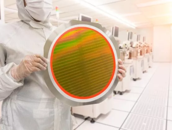
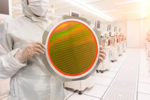
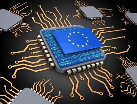
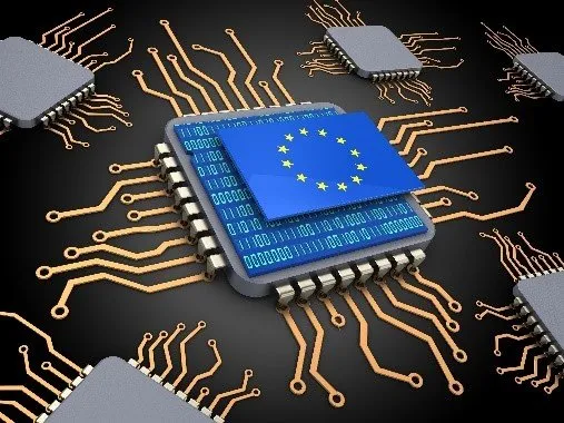
Semiconductors play an essential role in modern society by enabling ground-breaking technological advances. The manufacture of high-volume and advanced semiconductors requires the use of fluorinated chemicals known as PFAS. Representing the voice of SEMI members, I explained the important role of these substances and their “essential use” in the semiconductor manufacturing supply chain at a Chemical Watch conference for industry and European Union decision-makers on 3rd of December 2020.In order to achieve the European Green Deal’s zero pollution ambition for a toxic-free environment, the European Commission announced in its recently published Chemicals Strategy for Sustainability its intention to restrict the use of the most harmful chemicals, except in cases where they are deemed essential for society. Per- and polyfluoroalkyl substances – known as PFAS – are the first group of chemicals facing regulatory scrutiny on this basis. This begs the question: What chemicals should be characterized as essential for society and what uses will they encompass? The key and enabling role of semiconductors in modern lifeSemiconductors are essential and ubiquitous in our lives. They are integral to enabling modern society to function – driving advancements in mobile communication technologies for the smartphones and computers that help us work more efficiently and connect us with our loved ones. These benefits have never been more evident than in 2020 with billions of people finding themselves working and studying remotely and safely from home.At the same time, technologies relying on semiconductors have been vital in the effort to combat COVID-19 – in ventilators, medical imaging devices and digital healthcare solutions. In addition, semiconductors will also enable the next leap in society to Industry 4.0 and as essential building blocks in connected and electric vehicles, artificial intelligence (AI) and quantum computing.The Commissioner for Internal Market, Thierry Breton, has highlighted the strategic importance of semiconductors in achieving European digital sovereignty (for instance, in his speech at Hannover Messe Digital Days), and the EU’s New Industrial Strategy[1] also points to the importance of semiconductors and microelectronic systems. What must also be appreciated are the cost and complexity of producing these valuable technologies. Setting up a cutting-edge fabrication plant with the hundreds of pieces of semiconductor manufacturing equipment typically required can cost around €15 billion.[2] A single semiconductor manufacturing tool typically consists of millions of articles, and a typical fab may house several hundred pieces of equipment. Furthermore, according to SEMI estimates, the fabrication of semiconductor wafers requires approximately 500 highly specialized process chemicals. In many cases, these processes, equipment and facilities rely on the unique properties offered by PFAS.“SEMI has worked diligently to highlight the strategic importance of semiconductors in achieving European digital sovereignty, and we are pleased that the critical role of microelectronics has been fully recognized by the EU and Member States. Fluorinated chemicals are essential for semiconductor manufacturing. "These specific chemicals are necessary due to their unique properties, and no alternatives are currently available that can adequately provide the functional properties required in semiconductor manufacturing. The essential use concept, therefore, must enable technological innovation, must apply across the entire supply chain, and must enable EU’s critical infrastructure and strategic objectives.” What are PFAS, and why and where are they used in semiconductor manufacturing?PFAS are a broad and highly diverse group of substances with unique properties and characteristics. The Organisation for Economic Co-operation and Development (OECD) has compiled a list of approximately 4,700 substances,[3] a handful of which are used in the semiconductor manufacturing industry. These very specific chemicals are necessary due to their unique and unparalleled properties that enable them to be used in the demanding conditions of semiconductor manufacturing.Semiconductor chemicalsAt the very core of semiconductor manufacturing is the photolithography process, where microscopic geometric patterns are transferred onto a film or substrate. Photolithography specialty formulations containing fluorinated compounds are used in various steps of this process to ensure quality and reduce the probability of defects. PFAS must be used due to their low surface tension and compatibility with other chemicals. PFAS are typically no longer present in the finished product. However, there are applications where PFAS are present in the final semiconductor device, particularly in imaging semiconductors used in cameras, displays and some medical devices, amongst others. Semiconductor manufacturing equipmentPFAS are also essential to semiconductor manufacturing equipment and factory infrastructure. The exceptional combination of their heat and chemical resistance and their chemical inertness allows fluoropolymers to be used both in equipment components (tubing, gaskets, containers, filters, etc.) and lubrication (such as various oils and greases). These same properties are also needed to ensure the functioning of the surrounding infrastructure. Finally, some fluorinated gases, which are already regulated by specific legislation,[4] are used as refrigerants and to clean the facilities.These are a handful of examples of how PFAS are used in semiconductor manufacturing. Today, there is no other way to undertake these processes or to build semiconductor manufacturing equipment without PFAS. No alternatives are currently available that can adequately provide the functional properties required. Even if alternative chemicals and technologies were discovered today, due to the extremely complex qualification process throughout the value chain, it would take another 15 years to deploy them in high-volume manufacturing. Therefore, continued access to PFAS is a prerequisite for high-volume and advanced semiconductors. Lack of continued access to PFAS could lead to an inability to produce and supply the EU with semiconductor manufacturing technology.How should we think about essential uses?Regulators have started to think about what uses of PFAS are essential and in which cases their use should be allowed. In developing this concept, there are a few aspects to keep in mind.Essential use must enable, not hinder, technological innovationFirst and foremost, the essential uses concept should enable continued technological innovation instead of acting as a hindrance. Semiconductors and manufacturing technology are constantly evolving and becoming more diverse to help meet increasing societal demands. What we see as innovative today may be commonplace in the future, while future innovations may be unimaginable today. We must therefore be careful not to accidentally limit our future potential for innovation.Essential use must apply across the entire supply chainSecondly, classifying a use as essential should apply throughout the entire supply chain. We must, for example, avoid defining semiconductors as essential while classifying the semiconductor manufacturing equipment and chemicals used to produce semiconductors as not essential. In the semiconductor manufacturing supply chain, where one manufacturer can have up to 16,000 suppliers, this risk is evident.[5]Essential use must enable critical infrastructures and the EU’s strategic objectivesFinally, we should keep Europe’s societal priorities in mind. The EU needs to be able to maintain and protect its critical infrastructures. Similarly, we should not lose sight of the EU’s strategic objectives of a green and digital Europe.Semiconductors, in conjunction with their corresponding manufacturing equipment and chemicals, are essential technologies in everyday life and the backbone of the EU’s strategic value chains. Manufacturing semiconductors is a very expensive and complex process that would not be possible without the unique properties of PFAS, making them essential to achieving the EU’s strategic objectives today – whether the European Green Deal or digital autonomy – and in the future. Therefore, we must ensure that essential uses will enable the continued use of PFAS in semiconductor manufacturing.The SEMI presentation delivered at the Chemical Watch event can be accessed here.Emir Demircan is director of Public Policy and Advocacy at SEMI Europe.[1] “The EU will also support the development of key enabling technologies that are strategically important for Europe’s industrial future. These include robotics, microelectronics, high-performance computing and data cloud infrastructure, blockchain, quantum technologies, photonics [etc.]”[2] Emerging technologies in electronic components and systems (ECS) Opportunities Ahead – A study by DECISION, 2018 for the European Commission[3] Available here[4] Regulation (EU) No 517/2014, “F-Gas Regulation”[5] SIA Nathan Associates, 2016, https://www.semiconductors.org/wp-content/uploads/2018/06/SIA-Beyond-Borders-Report-FINAL-June-7.pdf
Read More
While Artificial Intelligence (AI) emerged in the 1950s, only in recent years have AI applications proliferated with the explosion of data and continuing improvements in Moore’s law that have driven rising processing speeds. Voice assistants, image analysis software, search engines, and speech and facial recognition systems were among the first applications to use AI. Today, adoption has spread to sectors such as agriculture, cybersecurity, healthcare, software development, e-government and the intelligent enterprise to generate jobs and help spur economic growth. The Edge AI Opportunity and the Microelectronics IndustryAI can be embedded in hardware devices such as advanced robots, autonomous cars, drones or Internet of Things (IoT) applications. Today, according to the EU’s digital strategy, data centres and other centralized computing facilities account for the vast majority – 80% – of AI data processing and analysis, with smart connected objects such as automobiles, home appliances and manufacturing robots that bring the compute function closer to the user representing 20%. The latter, known as Edge AI applications, are powered by edge-based machine learning chipsets, not the AI chipsets designed to run cloud-based machine learning algorithms.The EU’s white paper on AI published in February 2020 anticipates that the way data are stored and processed for AI applications will change significantly over the coming five years as edge computing applications proliferate. Most AI applications need to connect with devices that collect data and manage data flows. When the applications connect with cloud infrastructures to train large volumes of data for a machine learning model, the interface devices often require hardware support. Edge AI can minimize data transport by processing data directly from local devices to accelerate data analysis and decision-making and make data transport or accelerator hardware unnecessary, critical in reducing power consumption and enhancing data security for applications such as autonomous driving. Over the past 40 years, the ICT sector has been continuously increasing greenhouse gas (GHG) emissions despite efforts to shift to renewable energy. Cloud-based AI applications require an ICT infrastructure for high-performance computing and high-speed connectivity. According to MIT Technology Review, data centres’ AI workloads could account for a tenth of the world’s electricity usage by 2025. a mass update of cloud-based AI applications may significantly increase energy consumption, unlike with Edge AI. This is why the strategy for developing Edge AI is well-aligned with the EU’s Green Deal objectives. Europe aspires to play a leadership role in Edge AI to strengthen the sector’s competitiveness and protect the European digital sovereignty. Europe’s strong industrial competencies in embedded systems and microcontrollers will help the region promote development of European domestic AI solutions for emerging high-value IoT applications in industrial processes such as Industry 4.0, Connected and Automated driving (CSA), smart cities, climate action, healthcare, and national defence and security. With this strong strategic position in technology, Europe is well-positioned to invest to become the leader in the Edge AI global market.Preparing the Workforce for the Microelectronics IndustryTo design and manufacture leading Edge AI chipsets, European education providers and industry will need to work closely together to train the current and future workforces. Within the framework of the METIS project, a four-year project co-funded by the European Commission through the Erasmus+ programme, SEMI and imec deployed experts in the field to survey and interview focus groups. The survey identified the following key focus areas for workforce development: 1. True Capability of AI and Data Science With AI’s heavy dependence on data, the workforce of the future must be trained in areas of data science including data integrity to ensure quality, unbiased sourcing, collection and accurate analysis necessary to interpret huge volumes of data. Europe also needs to train the next generation of AI chip designers in data security and privacy – key challenges to the widespread deployment of Edge AI chips. 2. Climate Change, Sustainable Development Goals (SDGs) and Social Inclusion TrainingSince the industry must be able to develop Edge AI solutions to enable the digital transformation while limiting GHG emissions, microelectronics engineers need to be schooled in climate change and understand how their work contributes to meeting the United Nation’s Sustainable Development Goals (SDGs). Workplace diversity and social inclusion are also important target areas for education since Edge AI applications should serve various groups of people with different needs.3. EthicsChip industry workers must also be educated in ethical issues of AI related to the technology’s potential societal impact in the near future[1]. With AI applications capable of monitoring Internet searches based on users’ personal preferences and biases to deliver tailored advertising, news and other information, developers must recognize how the technology can influence thinking and behaviour of individuals and groups. This awareness can help developers strike a balance between supporting commercial interests and societal good so the microelectronics industry can ensure ethical implementation of AI. 4. Cross-disciplinary Skills Required for AIAI development requires a comprehensive, cross-disciplinary skill-set to be able to integrate the work of specialists from diverse educational, cultural and professional backgrounds critical to developing non-biased AI solutions. For example, in addition to technical expertise, microelectronics AI developers must be able to communicate clearly and work in close-knit teams with non-technical experts from business, law, medicine and the social sciences.What’s Next?The microelectronics industry has a tremendous opportunity to develop new chip-based solutions for AI architectures, and apply AI techniques to improve operational efficiencies of design and manufacturing. To seize this opportunity, the industry must work closely with education providers to groom the next generation of skilled workers. This tight collaboration is critical to designing and delivering specialised courses to college and university students as well as engineers now working in the chip sector. The stakes are high. By preparing workers to develop Edge AI chipsets, the microelectronics industry can help the world confront some of the greatest challenges it faces today.For more information, see SEMI Responds to European Commission White Paper on Artificial Intelligence.METIS is a Sector Skills Alliance project co-funded by the European Commission’s Erasmus+ Program and coordinated by SEMI. The four year project, launched in November 2019, will develop a Microelectronics Skills Strategy. Based on the strategy, the METIS project will design 43 training modules for 1,100 hours learning in four key areas of the microelectronics sector.We thank Patrick Blouet (STMicroelectronics) and Jeroen Geusens (imec) for their valuable contributions to this article.[1] Ethics of Artificial Intelligence and Robotics, Stanford Encyclopedia of PhilosophyDr. Yanying Li is senior manager of Collaborative Projects at SEMI Europe.Dr. Pushkar P. Apte is the strategic technology advisor for the Smart Data AI Initiative at SEMI
Read More
Europe is facing an acute shortage of skilled microelectronics workers that undermines the growth potential of not only the electronics industry but the European economy as a whole. Nearly 1.1 million job advertisements for electro-engineering workers were placed in the EU between mid-2018 and the end of 2019 (CEDEFOP, 2020). The shortfall looms large as a skilled and diverse workforce that can continuously innovate is the oxygen of microelectronics. In light of the critical importance of microelectronics to Europe’s ability to fulfill its growth potential, SEMI Europe participated in the high-level roundtable hosted by Commissioner Nicolas Schmit and Commissioner Thierry Breton on October 5. The discussion’s key takeaway: The skills challenge facing the microelectronics industry is too complex for one organization to tackle, and reskilling and upskilling its workforce should be a common priority for Europe. Only with a diverse, substantial and skilled microelectronics workforce can Europe achieve its R D, design and manufacturing ambitions while ensuring its sovereignty in the digital age. The roundtable highlighted the EU Pact for Skills as a key means to narrow the industry’s skills gap.An ever-growing part of our lives, microelectronics, with their ability to run billions of computations per second and store vast quantities of data, are the brains of modern technology. The digital sovereignty of nations around the world today relies on advanced microprocessors to collect, transfer, analyze and store immense amounts of data used in key end-user sectors such as mobility, telecommunications, energy, security and healthcare. Information and communication technologies (ICT) enabled by microelectronics are helping much of the world’s population to work and study from home and remain safe during the COVID-19 pandemic.According to the Smarter2030 Report, further deployment of ICT, including electronic components in critical sectors such as transportation, manufacturing, agriculture, construction and energy, could eliminate the equivalent of 12.1 billion tons of CO2 per year globally. These are some of the reasons why nations worldwide are making large-scale investments to advance a homegrown microelectronics R D, design and manufacturing base. It is no surprise, then, that semiconductors are now at the center of the so-called global techno-trade wars.Clearly, Europe urgently needs to mobilize and pool resources to develop effective lifelong learning programs for all workers and continue investing in microelectronics innovation. We need to instill the passion for creating technology among current and future workforce, in particular women and people with challenged backgrounds, and build a highly diverse talent pool. Working together, we can better demonstrate how computing technologies, including quantum, high-performance and edge AI, provide solutions to grand societal challenges and attract talented people to the fascinating world of electronic components and systems.Against this backdrop, the microelectronics industry finds the Pact for Skills very timely and crucial to advancing the talent pool underpinning Europe’s deep digital ecosystem. The Pact will play an instrumental role in improving the scope and the quality of training partnerships at regional, national and European levels, sharing best practices and helping the microelectronics industry and workforce adapt to the effects of COVID-19.The microelectronics industry is committed to building on the momentum created by the METIS Erasmus+ collaborative project and to mobilizing our ecosystem and education partners for a successful Pact for Skills in Microelectronics starting this year.The High-Level Roundtable: Skills for Microelectronics was hosted by Commissioner Thierry Breton and Commissioner Nicolas Schmit. Participants included Paul Boudre, CEO, SOITEC; Lars Reger, CEO Germany and CTO, NXP; Frits van Hout, Executive Vice-President and Chief Strategy Officer, ASML; Françoise Chombar, CEO, Melexis; Emmanuel Sabonnadiere, CEO, CEA-Leti; Luc Van den hove, President and CEO, imec; Sabine Nietzsche, Board member, Silicon Saxony and Vice President, GlobalFoundries; Laith Altimime, President, SEMI Europe (coordinator of METIS); Yolande Berbers, President, European Society for Engineering Education (SEFI); James Calleja, President, European Forum for Technical Vocational Education and Training (EFVET); Ludovic Voet, Confederal Secretary, European Trade Union Confederation (ETUC).Emir Demircan is director of Advocacy and Public Policy at SEMI Europe. To learn more about SEMI Europe advocacy, contact Emir at [email protected].
Read More
On 21 September, SEMI and a coalition of 40 industry organisations sent a letter to European Commission President Ursula von der Leyen calling for decisive action to solve implementation issues within the European Union Waste Framework Directive, specifically the Substances of Concern in Products (SCIP) database.The signatories, who represent a very significant part of the European economy, are requesting urgent resolution of implementation issues for the SCIP database, which is designed to support the circular economy as defined in the European Green Deal. The database is required under Article 9.1 of the updated Waste Framework Directive.In the letter, the signatories ask President von der Leyen to take immediate action to: Postpone the SCIP notification deadline of 5 January 2021 to at least one year after finalization of the database; Conduct a study on the usefulness, feasibility, proportionality and impact of the database; Instruct the European Chemicals Agency (ECHA) to adapt the SCIP database according to the outcome of the proposed study. ECHA failed to complete development of the database by the January 2020 deadline required by the Waste Framework Directive, leaving companies insufficient time to develop, test and adapt their own systems to meet the January 2021 SCIP notification deadline.Over the last two years, the signatories have repeatedly shared their serious concerns regarding the viability, proportionality and value of the SCIP database with the European Commission and the ECHA, yet those concerns remain unresolved.Contrary to the EU Better Regulation principles that call for open and transparent decision making, Article 9.1 was added to the revised Waste Framework Directive during the final stage of the co-decision process without any prior stakeholder consultation or impact assessment. A proper impact study should help shape the way forward to deliver on the EU ambition of driving a circular European economy.Coalition PartnersEmir Demircan is director of Advocacy and Public Policy at SEMI Europe.
Read More
METIS, a Sector Skills Alliance project co-funded by the European Commission’s Erasmus+ Program and coordinated by SEMI, recently launched an online questionnaire aimed at gauging the skills and expertise the industry needs to drive continued growth over the next five years. The survey, which will stay online until 15 October 2020, is a part of the METIS project’s efforts to involve a broad range of stakeholders in the microelectronics industry to assess workforce, future technology and economic trends influencing talent development and the skills needed most today and in the next five years. The survey aims to highlight the skill mismatches in specific job profiles that are of increasing importance to the microelectronics industry. It elaborates on the upskilling and reskilling needs for design engineers. Given that semiconductor design is becoming increasingly crucial for Europe’s competitiveness and technological sovereignty, the new skills required from design engineers are a priority area for the METIS project. Other examples are the manufacturing and maintenance technicians, two job profiles that are currently experiencing significant shifts in their skillsets, as COVID-19 has thoroughly transformed their way of work.While the microelectronics industry has been very aware of the importance of the high level of investment in R D, it is equally crucial to ensure that the workforce of the industry is equipped with knowledge and skills for the rapid technological developments. Maintaining high levels of investment in workforce including attracting talent, updating their knowledge and skills with the latest technological development, and supporting them to lead innovations, is essential for this industry. There is a growing demand for specific requirements for this sector to support innovation in many other sectors such as automotive, energy, healthcare, and government, to foster benefits from emerging digital technologies such as Cloud Services, Internet of Things (IoT), Artificial Intelligence (AI), Digital Reality, and Blockchain.In addition to the online questionnaire, the METIS project consortium is interviewing top experts from leading microelectronics companies, education representatives from universities and training academies, and experts from government agencies and industry associations. The interview outcomes provide inputs on what kind of employee profiles are the most difficult to find, what skills this sector is looking for in a candidate, and what kind of training and policy frameworks are needed to improve employers’ skills. Those inputs are essential to develop the skill strategy and form recommendations on training modules.Furthermore, the METIS project consortium is organizing 10 focus groups. Each of the focus groups is dedicated to a key topic, such as SC design, SC materials, semiconductor manufacturing equipment, etc. For example, one of the METIS focus groups is dedicated to Edge AI, a top priority for the microelectronics industry. Strengthening the AI talent pipeline is essential to harness the potential of Edge AI in Europe and to facilitate the shift from the Cloud to the Edge when possible in order to meet specific demands (e.g. for autonomous driving), reduce energy consumption for data communications, and to increase efficiency. The EU’s White Paper “Artificial Intelligence - A European approach to excellence and trust”[1] , published this February, also emphasizes the importance of upskilling and reskilling to position Europe among the global leaders in AI. Hence, the focus group will work towards pinpointing the skills necessary for the semiconductor workforce to capture the potential of the trend.The results of the survey, interviews and focus groups will be used to form the Microelectronics Skills Strategy. Based on this strategy, the METIS project will design 43 training modules for 1,100 hours learning in four key areas of the microelectronics sector:Component designSystem designBasic of manufacturingKey competencies and innovative thinkingThe METIS project is planning to recruit 2,000 learners in companies and education and training institutes to participate in the trainings and validate the impact. The METIS project will also work with companies, education and training providers to ensure continuity of the initiative and foster cooperation.During the METIS project course (2019 – 2023), the Skills Strategy will be updated yearly to reflect the latest technology and market trends. To enable the Skills Strategy to continue serving the industry, METIS is working on forming a permanent instrument, named Observatory and Skills Council, to continue developing the skills strategy, update the training and facilitate cooperation between industry and education and training providers.Laith Altimime, president of SEMI Europe, and 50 members of the Microelectronics Training, Industry and Skills (METIS) consortium The METIS consortium invites companies and associations involved in microelectronics training and education provision, human resources and career services professionals, technology strategists and policy makers to complete the online questionnaire. Stakeholders are also welcome to subscribe to the METIS newsletter for the latest on METIS programs. For more details, please contact Yanying Li at [email protected].[1] EU’s White Paper on Artificial Intelligence available at: https://ec.europa.eu/info/sites/info/files/commission-white-paper-artificial-intelligence-feb2020_en.pdfDr. Yanying Li is senior manager of Collaborative Projects at SEMI Europe.
Read More
On Monday, SEMI led a statement from a coalition of industry groups calling on governments worldwide to harmonize their policies to safely allow essential international travel by essential workers. Cross-border mobility in the semiconductor and microelectronics industry is vital to maintaining manufacturing critical to the production of semiconductor devices that are the foundation of our modern economy, countless economic sectors and each nation’s response to the COVID-19 pandemic. Uniform cross-border travel rules impacting essential businesses in the electronics supply chain are crucial for semiconductor business infrastructure and supply chains to maintain effective operations.To that end, SEMI is urging governments around the world to permit international travel by semiconductor supply chain engineers, technicians and executives with minimal disruption to ensure any fast-tracked procedures apply directly to the semiconductor industry and that any agreements negotiated among countries harmonize global travel procedures and processes. Global supply chains require cross-border travel by key technical personnel and business continuity decision-makers to ensure that essential industry manufacturing and business operations remain efficient, effective and uninterrupted. While the industry continues to implement safety protocols and minimize non-essential travel to stem the spread of COVID-19, highly sophisticated equipment sets and materials usage from multiple nations will at times require specialized expertise that is not present in-country.For example, technicians from a semiconductor manufacturing equipment company typically must travel to semiconductor factories in other countries to install or repair specialized tools in situations that are beyond the expertise of the local field office and too complicated to handle by video conference. Similarly, at times semiconductor-based solutions, such as cloud computing, must be implemented or optimized on-site for the equipment to achieve full capacity. After months of remote access to their overseas operations, it also is critical that executives are able to visit their facilities to evaluate and manage their ongoing operations. In the past month, several countries central to the global electronics supply chain have engaged in both formal and informal talks to ease travel restrictions on personnel from essential industries. China, for example, is negotiating fast-track travel protocols with countries throughout Asia and Europe. On May 1, China and South Korea formalized an agreement that has made significant accommodations for semiconductor industry personnel to travel between the two countries. Last week, China and Singapore reached a similar deal – planned to take effect in early June – prioritizing travel for both executives and technicians.Beyond China, several ad-hoc negotiations are underway involving countries as varied as Taiwan, Vietnam, South Korea, Thailand, Canada, Australia and New Zealand. Multilateral discussions are also afoot with the aim of setting up bubble travel zones featuring standard health and travel protocols within the country blocs. As these disparate agreements between individual countries or small blocs of countries take shape, however, they are likely to create divergent standards that may complicate efforts of global businesses to effectively service their operations and customers, even if such travel is and has been deemed essential.In March, when U.S. states and many governments around the world began implementing stay-at-home orders and closing non-essential business operations, SEMI immediately took a lead role advocating to ensure that that the entire microelectronics supply chain was deemed essential and able to continue operations. In the U.S., nearly every state followed SEMI’s recommendation to adhere to the Department of Homeland Security’s Cybersecurity and Infrastructure Security Agency (CISA) guidelines that included semiconductor manufacturing and its supply chain as essential, or specifically highlighted semiconductor supply chains as essential. Overseas, SEMI advocacy worked to ensure the semiconductor supply chain was deemed essential in every key jurisdiction.The mobility of essential workers is critical to essential business operations in the electronics supply chain. Just as SEMI led the effort to ensure that critical electronics supply chain operations were deemed essential as economies were closing down, SEMI will continue to advocate for uniform essential travel guidelines for critical infrastructure workers as economies reopen. Karl Kailing is manager of Public Policy and Advocacy at SEMI.
Read More
In an important step toward resuming business as usual in Japan, Prime Minister Shinzo Abe on May 14 lifted the state of emergency originally scheduled to expire at the end of May for 39 of Japan’s 47 prefectures, marking “the real beginning of our efforts toward a new normal in the era of the coronavirus” as new cases continue to decline. But with Tokyo, Osaka and six other prefectures still under the state of emergency, Abe urged citizens to remain cautious as the nation and world continue to confront the COVID-19 threat. Among criteria the remaining prefectures must meet for a state of emergency suspension is a reduction in new infections to no more than 0.5 cases weekly for every 100,000 citizens. The eight prefectures account for nearly half of Japan’s population and GDP, with Tokyo and Osaka the two largest urban areas in the island nation. Japan expects to contain its economic losses to 38 trillion yen, 15 percent less than the 45 trillion yen hit originally projected. The Japan government has planned a May 21 progress review[1] in the eight prefectures, a timeline that Abe said could lead to the lifting of the state of emergency before the original cutoff at the end of the month, a move that would help stem the drain on the domestic economy.Strict Immigration Controls Restricts International Travel to and from Japan by Supplier EngineersAs I reported on April 21, the Japan Foreign Ministry on March 31 raised its travel advisory to level 3 for 49 regions around the world including the U.S., prohibiting travel from Japan for any purpose. SEMI Japan is urging government officials to exempt Japanese supply chain engineers from the travel ban to allow visits to semiconductor manufacturing facilities in those regions in order to install, start up and service equipment.Starting May 14, Japan blocked immigration of foreign nationals and permanent residents from 100 countries and regions worldwide, a ban applying to anyone who spent time in their home region within 14 days of their planned arrival in Japan. The areas include China, Singapore, South Korea, and Taiwan in Asia; Canada and the U.S.; and Germany, France, Italy, Netherlands, Switzerland and the U.K. in Europe. For the complete list, see the Japan Ministry of Justice’s website.Japan’s immigration ban mirrors restrictions now in place in many other regions around the world. The immigration controls are well-intended – to restrict the spread of COVID-19 – but hamstring the global microelectronics supply chain. For example, the curbs bar engineers from international travel to install new tools and software in fabs. SEMI Japan has stressed the potential chip industry impacts of the ban in ongoing talks with the Ministry of Economy, Trade and Industry and is facilitating discussions between government representatives and SEMI members to help clear the way for travel by critical supply chain workers to Japan. SEMI Supports Members with COVID-19 ResourcesSEMI international headquarters and regional offices are here to help you, our members. For more information on our webinars, surveys, best practices and other information designed to help you meet the challenges of the pandemic, please visit the SEMI Coronavirus Updates Resources page.[1] The May 21 review found three prefectures in western area – Hyogo, Kyoto and Osaka – met the criteria to lift the state of the emergency. Four other prefectures – Chiba, Hokkaido, Saitama and Tokyo – remain under the emergency order that will be reviewed again as early as May 25.Jim Hamajima is president of SEMI Japan.
Read More