downloadGroupGroupnoun_press release_995423_000000 copyGroupnoun_Feed_96767_000000Group 19noun_pictures_1817522_000000Member company iconResource item iconStore item iconGroup 19Group 19noun_Photo_2085192_000000 Copynoun_presentation_2096081_000000Group 19Group Copy 7noun_webinar_692730_000000Path
Skip to main content
Default Banner Image

ASML

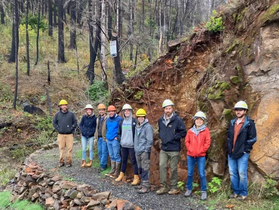
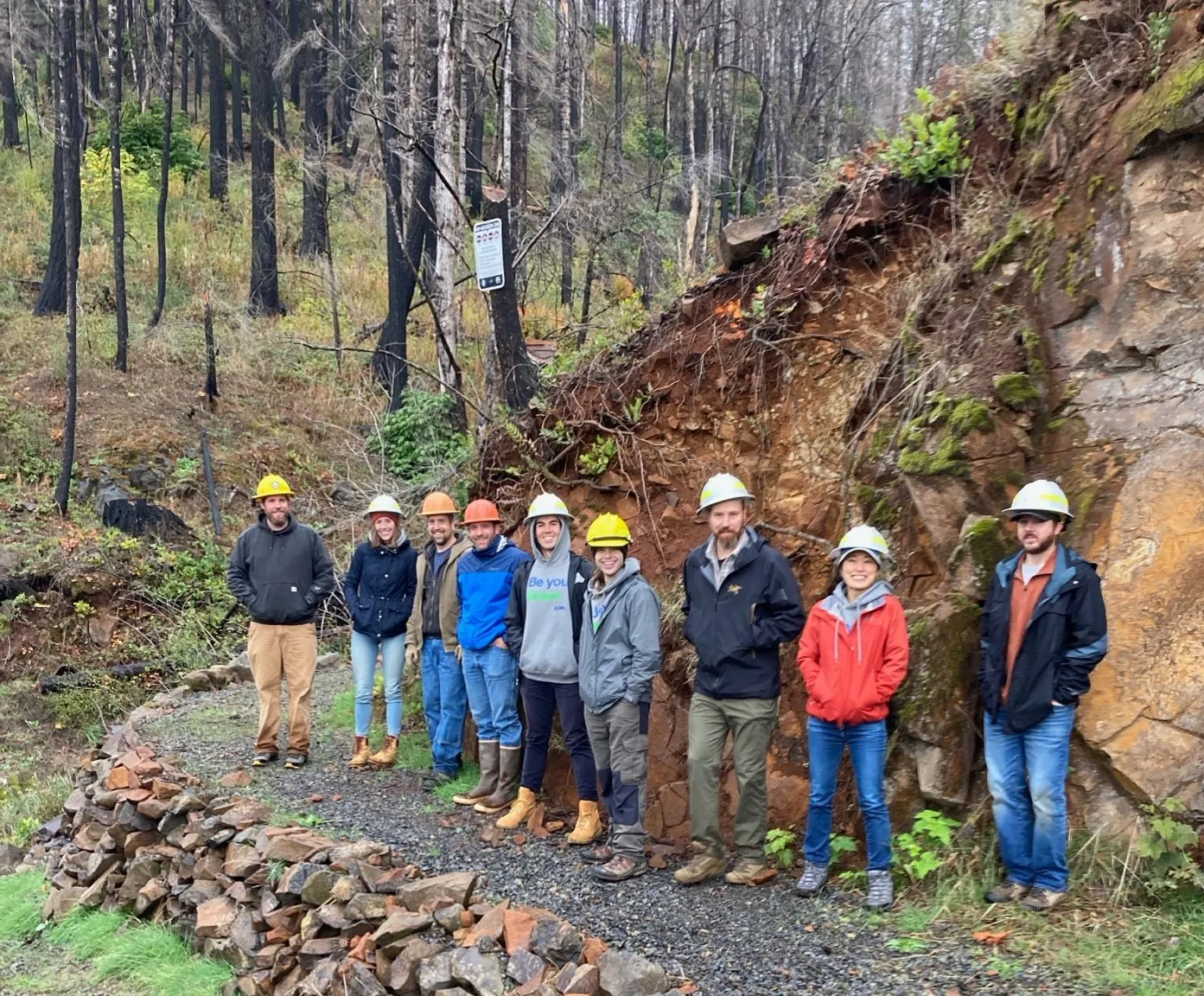
Gregory Woods, leader of the San Diego-based Green ASML employee group, stands with the tree-planting team at the Santiam State Forest site in Oregon, October 2023.Photo Credit: Dave Laegen, veritreeA tree-planter is geared up for a day of restoration, a result of the public-private partnership with American Forests and the Oregon Department of Forestry.https://veritree.mediavalet.com/portals/OregonOverviewForests hold the natural world together…. They are the ecosystem engineers that create the conditions for other forms of life to exist, on every level.— Jim Robbins, “The Man Who Planted Trees”Climate-driven events like fire and smoke events are becoming increasingly common along the Pacific coast, from British Columbia to California. In the wake of the 2020 “Labor Day” wildfires that devastated large parts of Oregon, a US employee network group at ASML, a leading player in the semiconductor industry, sought an innovative way to contribute to restoring the environment and sequester carbon. This commitment led to a partnership with veritree, a technology-driven reforestation organization, resulting in a groundbreaking initiative — starting with 40,000 trees.The ChallengeDuring an interview for this story, Markus Matthes, former Site Lead at ASML San Diego, current Head of ASML Germany and Chairman of the Berlin Management Team and sponsor of the local employee-led network, noted that in light of the semiconductor industry’s energy consumption and chemical inputs, “I was pleased to support this proactive approach from the local employee network group. At ASML, we feel it is important to play our part in addressing key environmental and social concerns that we share with our stakeholders.” Over the last 3-5 years, companies in the semiconductor value chain have strived to collaboratively identify critical steps on the path to net zero emissions through industry alliances like the SEMI Climate Consortium.Green ASML San Diego, an employee network group (ENG) led by Gregory Woods, Senior Systems Industrialisation Engineer and Chair of Green ASML San Diego, decided a proactive approach to giving back could be to help restore the forests that Oregon lost 4 years ago. But they wanted to make a meaningful environmental impact, ensuring transparency and accountability while also advancing carbon sequestration efforts. With reforestation as the focus, the challenge was identifying a partner capable of delivering measurable, long-term results while providing visibility into the process. This was a sticking point for Matthes, who affirmed that “we do not want to do window dressing in terms of planting trees … we also want to have evidence that it’s really working, that trees are really growing, that they are storing CO2, etc.”The SolutionThe idea to plant ‘one tree per employee’ began with Woods and Green ASML San Diego before quickly gaining executive sponsorship. Matthes expressed pride in the San Diego Green Team and attributed the success of the program to their persistence. Where he and Martin Reinecke, Head of Cymer Business Planning and Operations, Cymer Light Sources San Diego, came into play as the executive sponsors in guiding how to get the project funded: “typically we know the folks in the headquarters. We know how to approach them. And then we can also perhaps help in making a catchy story.”More than just a catchy story, partnering with veritree made for a sound pitch. They stood out among other reforestation providers due to their innovative assemblage of GIS, blockchain, and sensor technologies. This approach ensures every tree planted is verified, monitored, and accounted for over time. With support from ASML’s leadership, Green ASML San Diego partnered with veritree to restore 40,000 trees — one per each of ASML’s 40,000 employees — to an area near ASML Hillsboro, that was heavily impacted by Oregon’s Labor Day fires.By leveraging this technology, veritree provides real-time updates on the health of the ASML forest and its long-term project outcomes. ASML has benefitted from access to real-time project data, which have reinforced trust and engagement among stakeholders while setting a high standard for nature-based carbon removal projects. As Matthes put it, “here Mother Nature is doing most of the work. We are just observing and checking ... we really have evidence that it’s really doing something good.”ResultsThis partnership is not only bringing back life to the fire-damaged landscape but also demonstrates how technology can enhance transparency in environmental initiatives. For SEMI companies with similar aspirations, Matthes highlighted one benefit of supporting ENGs is that their success “radiates back into the organization itself.” He said initiatives like this act as an “intrinsic motivator.” Woods added that it creates a positive sentiment within the company that “ENGs with the right ideas, with the right enthusiasm ... can actually make a difference.”Through their collaboration with veritree, Green ASML San Diego turned a spark of inspiration into a powerful movement, offering a replicable model for other corporations. To achieve these results, Matthes recommended that fellow SEMI companies should “trust your ENG” and “try to place it … as a combination of a grassroots initiative with some strong executive support.” Starting with a simple ‘one tree per employee’ concept, ASML was able to scale the idea into a significant environmental initiative. With Woods’ vision of growing the ASML forest from 40,000 to 3 million trees over the next few years, the movement continues.Key Project MetricsAll data related to the trees is accessible via ASML’s Impact Hub2 public partners: Oregon Department of Forestry and American Forests40,000 trees planted: Douglas-fir, Noble Fir, Western Red CedarCarbon sequestration: 23.1k tons of CO2 over lifetime of treesEcological impact: 26.68 hectares restoredEconomic impact: 160 work days provided“The How”: Recommended action steps for achieving broad buy-inCarbon removal highlighted as a focus area for Green ASML San Diego throughout 2022Green ASML (Employee Network/Resource Group) met with potential partner veritree to learn about planting methodology, sites and how to start partnershipGreen ASML San Diego chapter presents the project to local executive sponsors and global Green ASML sponsor (ASML Executive Committee member). Received unwavering support to move forward and “ASML pledges to plant 40,000 trees for holiday season ’22, planting one tree for every employee and celebrating its drive to pioneer sustainable semiconductor manufacturing.”Post-fire restoration project in Oregon, USA chosen as planting site for local community engagement (ASML Hillsboro and Intel Corporation)Memorandum of Understanding (MOU) signed by ASML Procurement team and veritree in Oct-Nov 2022In April 2023, the 40,000 trees were allocated to ASML from a 200,000 initial planting roundRestoration initiative recommended to be communicated as US-driven project, instead of a global ESG initiative, since it did not meet certain carbon offsetting criteriaImpact data, GPS coordinates and field reports (Survivability Assessment) provided for verification from veritreeGreen ASML San Diego board visited Oregon planting site with veritree team, American Forests (NGO) and Oregon Department of Forestry in Oct. 2023Impact Hub showcases ~716.10 tons of CO2 sequestered from year 1 (Dec. 31, 2023)Green ASML continued prioritization towards restoration/reforestation projects throughout 2024 and how to expand with veritreeIn 2024, an additional 7,452 trees were funded to be planted in Oregon, USA plus 5,000 mangrove trees were funded in KenyaAbout the Author:Nat Mengist is a PhD student in Learning Sciences at the University of Washington. He recently earned a master’s degree in Human Centered Design and Engineering and he serves on the executive board of the Society for Literature, Science, and the Arts. As a storyteller, Nat has created multimedia science fiction about the future of climate justice. This article was a team effort, written on behalf of veritree and the SEMI Sustainability Initiative.
Read More
Europe is facing an acute shortage of skilled microelectronics workers that undermines the growth potential of not only the electronics industry but the European economy as a whole. Nearly 1.1 million job advertisements for electro-engineering workers were placed in the EU between mid-2018 and the end of 2019 (CEDEFOP, 2020). The shortfall looms large as a skilled and diverse workforce that can continuously innovate is the oxygen of microelectronics. In light of the critical importance of microelectronics to Europe’s ability to fulfill its growth potential, SEMI Europe participated in the high-level roundtable hosted by Commissioner Nicolas Schmit and Commissioner Thierry Breton on October 5. The discussion’s key takeaway: The skills challenge facing the microelectronics industry is too complex for one organization to tackle, and reskilling and upskilling its workforce should be a common priority for Europe. Only with a diverse, substantial and skilled microelectronics workforce can Europe achieve its R D, design and manufacturing ambitions while ensuring its sovereignty in the digital age. The roundtable highlighted the EU Pact for Skills as a key means to narrow the industry’s skills gap.An ever-growing part of our lives, microelectronics, with their ability to run billions of computations per second and store vast quantities of data, are the brains of modern technology. The digital sovereignty of nations around the world today relies on advanced microprocessors to collect, transfer, analyze and store immense amounts of data used in key end-user sectors such as mobility, telecommunications, energy, security and healthcare. Information and communication technologies (ICT) enabled by microelectronics are helping much of the world’s population to work and study from home and remain safe during the COVID-19 pandemic.According to the Smarter2030 Report, further deployment of ICT, including electronic components in critical sectors such as transportation, manufacturing, agriculture, construction and energy, could eliminate the equivalent of 12.1 billion tons of CO2 per year globally. These are some of the reasons why nations worldwide are making large-scale investments to advance a homegrown microelectronics R D, design and manufacturing base. It is no surprise, then, that semiconductors are now at the center of the so-called global techno-trade wars.Clearly, Europe urgently needs to mobilize and pool resources to develop effective lifelong learning programs for all workers and continue investing in microelectronics innovation. We need to instill the passion for creating technology among current and future workforce, in particular women and people with challenged backgrounds, and build a highly diverse talent pool. Working together, we can better demonstrate how computing technologies, including quantum, high-performance and edge AI, provide solutions to grand societal challenges and attract talented people to the fascinating world of electronic components and systems.Against this backdrop, the microelectronics industry finds the Pact for Skills very timely and crucial to advancing the talent pool underpinning Europe’s deep digital ecosystem. The Pact will play an instrumental role in improving the scope and the quality of training partnerships at regional, national and European levels, sharing best practices and helping the microelectronics industry and workforce adapt to the effects of COVID-19.The microelectronics industry is committed to building on the momentum created by the METIS Erasmus+ collaborative project and to mobilizing our ecosystem and education partners for a successful Pact for Skills in Microelectronics starting this year.The High-Level Roundtable: Skills for Microelectronics was hosted by Commissioner Thierry Breton and Commissioner Nicolas Schmit. Participants included Paul Boudre, CEO, SOITEC; Lars Reger, CEO Germany and CTO, NXP; Frits van Hout, Executive Vice-President and Chief Strategy Officer, ASML; Françoise Chombar, CEO, Melexis; Emmanuel Sabonnadiere, CEO, CEA-Leti; Luc Van den hove, President and CEO, imec; Sabine Nietzsche, Board member, Silicon Saxony and Vice President, GlobalFoundries; Laith Altimime, President, SEMI Europe (coordinator of METIS); Yolande Berbers, President, European Society for Engineering Education (SEFI); James Calleja, President, European Forum for Technical Vocational Education and Training (EFVET); Ludovic Voet, Confederal Secretary, European Trade Union Confederation (ETUC).Emir Demircan is director of Advocacy and Public Policy at SEMI Europe. To learn more about SEMI Europe advocacy, contact Emir at [email protected].
Read More
Like so much else these days, career mentoring in the semiconductor industry has gone virtual. And, among hiring managers, for good reason: Chip companies are facing a new urgency to hire skilled workers as recent SEMI forecasts spanning packaging materials and fab equipment spending show strong growth in 2021 – a trajectory that puts even more pressure on an industry confronted with a worker shortage to attract and recruit new talent.Enter SEMI Korea, which early this month gathered nearly 4,000 sheltered-in-place South Korea university students to offer tips from semiconductor industry insiders on how to kick-start their careers in the chip business. In 14 sessions over three days, industry powerhouses offered guidance across topics ranging from educational preparation and job skills to resume writing and interviewing. Like last year’s on-site event, students from Seoul accounted for the bulk of those online for Campus Outreach On-Air. But this year saw a far higher turnout of students in provincial cities thanks to the ease and convenience of virtual communications – a silver lining in the age of COVID-19.Establishing a successful career in the semiconductor industry starts with a mix of soft and hard skills, according to Changjin Kang, CEO of SEMES, one of the top 10 global semiconductor equipment companies. Keynoting the event, Kang pointed to six key attributes in particular – caring, resilience, execution, analysis, tenacity and experience – under the acronym C.R.E.A.T.E.Caring means empathy for colleagues, understanding their unique work environment and challenges, and building strong relationships. To help cope with the stress that can come with working in the industry, workers must be also be resilient by managing the emotional demands of a job and getting enough rest. Execution comes down to thorough, methodical planning. Carefully analyzing information to make data-driven decisions is a critical aspect of successful outcomes, while having the tenacity to push through difficult technical challenges helps engineers develop the right solutions. And getting out from behind the desk to learn from colleagues is important in building experience.Human resources representatives and engineers from Applied Materials, ASML, Dongjin Semichem, EO Technics, Jusung Engineering, KLA, Lam Research, Merck KGaA, Darmstadt, Germany, PSK, SEMES, SK Siltron, TEL and Wonik IPS shared with the students the key competencies needed to forge a career in the semiconductor industry. Engineers pointed to the benefits of improving their English skills through language training and continuing their education by pursuing engineering certificates. Human resources representatives stressed the importance of a global mindset since, as part of the global semiconductor ecosystem, engineers and other staff often communicate via conference calls with colleagues around the world.In a post-event survey, the students – all digital natives – awarded the event 4.3 out of 5 points for overall satisfaction and made clear that they prefer online Campus Outreach to the on-site event.“Thanks to SEMI and the companies for providing a great opportunity to meet experts and HR managers,” one student pointed out in the survey. “It was very useful because it opened up opportunities for many students to communicate with semiconductor companies.”“It was nice to know what works semiconductor engineers do,” said another, “and how as university students they prepared for employment.”SEMI Korea thanks the nine semiconductor companies that sponsored Campus Outreach On-Air to help build the industry’s talent pipeline and the students for their invaluable participation.Jaegwan Shim is a marketing specialist at SEMI Korea.
Read More
What’s next for smarter, more connected electronics manufacturing - Part 3 The fast-maturing infrastructure now enabling analysis of exponentially larger data volumes brings the microelectronics industry to an inflection point, where the winning companies will be the first to master the use of this data to solve the industry’s emerging challenges. SEMI expands its coverage of these vital issues with a Smart Manufacturing Pavilion and three days of talks SEMICON West, July 10-12 in San Francisco. While deep learning is starting to be applied to image recognition for wafer inspection, it is also being considered for sequential pattern recognition in order to evaluate equipment parameter traces. The next emerging applications will start to use those learned patterns to predict outcomes, and then use those predictions to automate process control. One early application of deep learning is IC process development. “People don’t think of research and development as the first place to automate, but it’s where applying our digitization and simulation has first had impact,” says David Fried, Coventor vice president of Computational Products. He noted that insertion is easier in the lab than in the fab. Technology at 10nm and beyond is now so complex that companies at the leading edge must use process modeling to understand the effect of process variation on their designs. Learning cycles can now be accelerated during development by simulating 10,000 digital wafers instead of running 25 actual wafers during screening, Fried says. Applying structured analysis and machine learning to the data simplifies optimization across the 500 or more interrelated process steps. Coventor has recently introduced a statistical analysis package that aids the design and analysis of process variation experiments by using large volumes of data from its models. Fried says these models are next being used to accelerate the yield ramp in manufacturing. Digital simulation also could speed development of high-mix, lower value products While digital twins are best known for their use in complex, high value products like jet engines, the simulation technology could also enable the electronic manufacturing services (EMS) sector to reduce the time, cost and risk of developing its high mix of products. “The EMS sector’s use of digital twins will be vital for it to smooth the move of CAD/CAM digital design data for so many different products into manufacturing, and to accelerate validation testing of designs and products by doing more of it in the virtual world,” says Dan Gamota, vice president of Engineering and Technical Services at Jabil. Gamota also highlights the push for traceability from the automotive and healthcare markets, where the digital models could be used to quickly assure that the design was built exactly as specified. “In the past year, traceability has evolved from just ‘nice to have’ to ‘how to achieve,’” he adds. “Companies are expecting it, but aren’t willing to accept the cost and risk of doing it alone. We need the community to discuss realistic implementations, identify the most critical elements and bring together the ecosystem partners to build baseline reference architectures for key digital building blocks. The community also needs to assure the reliable flow of data among the electronic manufacturing segments from semiconductor to OSAT to EMS.” Predictive maintenance and virtual metrology applications could mature in next few years While predictive maintenance initially seemed a likely early application of machine learning in factories, it remains a challenge for the electronics sector. “The difficulty is that it’s not clear where to get the most bang for the buck,” says Tom Ho, president of BISTel America, noting that it may make the most sense to track the failure performance of a single expensive part, like an electrostatic chuck, since predicting the failure performance of a whole complex system like an etcher is much harder. “Collecting enough data from all failure types, including especially the rare events, is difficult unless you have a long history of a lot of tools,” adds Doug Suerich, PEER Group product evangelist. “The gain from collecting performance information from many tools across the industry could be big, but many companies still need to overcome concerns around exposing their IP.” Another big opportunity for prediction is virtual metrology – predicting the wafer outcome from the process or sensor data with enough accuracy to replace the physical metrology. “Virtual metrology is improving, and since metrology can be slow and expensive, any reduction could mean a huge potential savings,” says Suerich. “But it is still seen as too scary for many companies. Two to three years from now, companies will expand the practice from lower risk areas into processes that require more confidence in the results.” Moving beyond prediction to automated control needs digital models Once the results are predicted, the model can be used to control or automatically optimize a process and enable the system to learn by itself, usually by reinforcement learning on a digital model. The model can then independently make adjustments to optimize the manufacturing process. “Automated process development is getting close now. Instead of smart guys turning the knobs, deep learning is automating the smart tuning,” says Suerich, suggesting the industry could see widespread adoption in as little as two to three years. This type of machine learning needs a good digital model, and masses of data for learning. One approach uses human experts to build a physics-based model of the clearly understood parts of the process, then turns to deep machine learning to optimize the lesser-understood variables. The alternative, the data-first approach, runs a computer algorithm to suggest the solution purely from data, without human input, and then relies on the human to evaluate the usefulness of the results. Modeling digital twins of wafers could enable automated process control, chamber matching, and fleet matching, says Fried. If every wafer had its own virtual twin with all the upstream metrology and structural information needed to make equipment control decisions, it could feed forward that information to enable the seamless transition from one step in the process to another based on understanding their complex interrelationships. This could potentially improve uniformity across wafers and equipment, and reduce the need for metrology, he argues. Moving metrology sensors into the chamber will also require model-based algorithms to enable dynamic process control in close to real time, says Fried. These algorithms will be needed to acquire, parse, and process the data at high speed, and then to choose how to adjust the controls. “There will be a model behind collecting and interpreting the metrology data,” he notes. “That’s a really rich vein for improvements in process control.” “The end goal is to collect equipment data in real time, analyze it with AI, and send back controls to optimize manufacturing processes,” Jabil’s Gamota says. “This requires a robust architecture for communication between equipment and consistent formats for data collection and analysis. But the cost and complexity of this heavy lifting is too great for any one company to do alone. We need a consensus-based architecture for ingesting, analyzing and acting on the data.” SEMI tests data transfer protocols, benchmarks best practices SEMI is launching a smart data project to identify the various data transfer protocols needed for inter-company communications. The project will feature a proof-of-concept model in a development fab to produce verifiable results so SEMI can better understand how different approaches meet member needs. SEMI’s smart manufacturing technology communities and the Fab Owners Alliance are also benchmarking current smart manufacturing practices in the microelectronics industry to help SEMI members better understand the path forward and potential return on investment. Speakers over all three days at SEMICON West addressing these issues include Active Layer Parametrics, Applied Materials, Applied Research Photonics, ASML, Bosch Rexroth, Cimetrix, Coventor, ECI Technologies, Edwards Vacuum, Final Phase Systems, GE Digital, Infineon, Jabil, Lam Research, Osaro, Otosense, PEER Group, Qualcomm, Rockwell Automation, Rudolph Technologies, Schneider Electric, Seagate, Siemens, Stanford University, TEL, TIBCO Software. See semiconwest.org. What’s next for smarter, more connected electronics manufacturing - Part 1 What’s next for smarter, more connected electronics manufacturing - Part 2 Paula Doe, SEMI
Read More