downloadGroupGroupnoun_press release_995423_000000 copyGroupnoun_Feed_96767_000000Group 19noun_pictures_1817522_000000Member company iconResource item iconStore item iconGroup 19Group 19noun_Photo_2085192_000000 Copynoun_presentation_2096081_000000Group 19Group Copy 7noun_webinar_692730_000000Path
Skip to main content
Default Banner Image

AI

Semiconductors play an essential role in modern society by enabling ground-breaking technological advances. The manufacture of high-volume and advanced semiconductors requires the use of fluorinated chemicals known as PFAS. Representing the voice of SEMI members, I explained the important role of these substances and their “essential use” in the semiconductor manufacturing supply chain at a Chemical Watch conference for industry and European Union decision-makers on 3rd of December 2020.In order to achieve the European Green Deal’s zero pollution ambition for a toxic-free environment, the European Commission announced in its recently published Chemicals Strategy for Sustainability its intention to restrict the use of the most harmful chemicals, except in cases where they are deemed essential for society. Per- and polyfluoroalkyl substances – known as PFAS – are the first group of chemicals facing regulatory scrutiny on this basis. This begs the question: What chemicals should be characterized as essential for society and what uses will they encompass? The key and enabling role of semiconductors in modern lifeSemiconductors are essential and ubiquitous in our lives. They are integral to enabling modern society to function – driving advancements in mobile communication technologies for the smartphones and computers that help us work more efficiently and connect us with our loved ones. These benefits have never been more evident than in 2020 with billions of people finding themselves working and studying remotely and safely from home.At the same time, technologies relying on semiconductors have been vital in the effort to combat COVID-19 – in ventilators, medical imaging devices and digital healthcare solutions. In addition, semiconductors will also enable the next leap in society to Industry 4.0 and as essential building blocks in connected and electric vehicles, artificial intelligence (AI) and quantum computing.The Commissioner for Internal Market, Thierry Breton, has highlighted the strategic importance of semiconductors in achieving European digital sovereignty (for instance, in his speech at Hannover Messe Digital Days), and the EU’s New Industrial Strategy[1] also points to the importance of semiconductors and microelectronic systems. What must also be appreciated are the cost and complexity of producing these valuable technologies. Setting up a cutting-edge fabrication plant with the hundreds of pieces of semiconductor manufacturing equipment typically required can cost around €15 billion.[2] A single semiconductor manufacturing tool typically consists of millions of articles, and a typical fab may house several hundred pieces of equipment. Furthermore, according to SEMI estimates, the fabrication of semiconductor wafers requires approximately 500 highly specialized process chemicals. In many cases, these processes, equipment and facilities rely on the unique properties offered by PFAS.“SEMI has worked diligently to highlight the strategic importance of semiconductors in achieving European digital sovereignty, and we are pleased that the critical role of microelectronics has been fully recognized by the EU and Member States. Fluorinated chemicals are essential for semiconductor manufacturing. "These specific chemicals are necessary due to their unique properties, and no alternatives are currently available that can adequately provide the functional properties required in semiconductor manufacturing. The essential use concept, therefore, must enable technological innovation, must apply across the entire supply chain, and must enable EU’s critical infrastructure and strategic objectives.” What are PFAS, and why and where are they used in semiconductor manufacturing?PFAS are a broad and highly diverse group of substances with unique properties and characteristics. The Organisation for Economic Co-operation and Development (OECD) has compiled a list of approximately 4,700 substances,[3] a handful of which are used in the semiconductor manufacturing industry. These very specific chemicals are necessary due to their unique and unparalleled properties that enable them to be used in the demanding conditions of semiconductor manufacturing.Semiconductor chemicalsAt the very core of semiconductor manufacturing is the photolithography process, where microscopic geometric patterns are transferred onto a film or substrate. Photolithography specialty formulations containing fluorinated compounds are used in various steps of this process to ensure quality and reduce the probability of defects. PFAS must be used due to their low surface tension and compatibility with other chemicals. PFAS are typically no longer present in the finished product. However, there are applications where PFAS are present in the final semiconductor device, particularly in imaging semiconductors used in cameras, displays and some medical devices, amongst others. Semiconductor manufacturing equipmentPFAS are also essential to semiconductor manufacturing equipment and factory infrastructure. The exceptional combination of their heat and chemical resistance and their chemical inertness allows fluoropolymers to be used both in equipment components (tubing, gaskets, containers, filters, etc.) and lubrication (such as various oils and greases). These same properties are also needed to ensure the functioning of the surrounding infrastructure. Finally, some fluorinated gases, which are already regulated by specific legislation,[4] are used as refrigerants and to clean the facilities.These are a handful of examples of how PFAS are used in semiconductor manufacturing. Today, there is no other way to undertake these processes or to build semiconductor manufacturing equipment without PFAS. No alternatives are currently available that can adequately provide the functional properties required. Even if alternative chemicals and technologies were discovered today, due to the extremely complex qualification process throughout the value chain, it would take another 15 years to deploy them in high-volume manufacturing. Therefore, continued access to PFAS is a prerequisite for high-volume and advanced semiconductors. Lack of continued access to PFAS could lead to an inability to produce and supply the EU with semiconductor manufacturing technology.How should we think about essential uses?Regulators have started to think about what uses of PFAS are essential and in which cases their use should be allowed. In developing this concept, there are a few aspects to keep in mind.Essential use must enable, not hinder, technological innovationFirst and foremost, the essential uses concept should enable continued technological innovation instead of acting as a hindrance. Semiconductors and manufacturing technology are constantly evolving and becoming more diverse to help meet increasing societal demands. What we see as innovative today may be commonplace in the future, while future innovations may be unimaginable today. We must therefore be careful not to accidentally limit our future potential for innovation.Essential use must apply across the entire supply chainSecondly, classifying a use as essential should apply throughout the entire supply chain. We must, for example, avoid defining semiconductors as essential while classifying the semiconductor manufacturing equipment and chemicals used to produce semiconductors as not essential. In the semiconductor manufacturing supply chain, where one manufacturer can have up to 16,000 suppliers, this risk is evident.[5]Essential use must enable critical infrastructures and the EU’s strategic objectivesFinally, we should keep Europe’s societal priorities in mind. The EU needs to be able to maintain and protect its critical infrastructures. Similarly, we should not lose sight of the EU’s strategic objectives of a green and digital Europe.Semiconductors, in conjunction with their corresponding manufacturing equipment and chemicals, are essential technologies in everyday life and the backbone of the EU’s strategic value chains. Manufacturing semiconductors is a very expensive and complex process that would not be possible without the unique properties of PFAS, making them essential to achieving the EU’s strategic objectives today – whether the European Green Deal or digital autonomy – and in the future. Therefore, we must ensure that essential uses will enable the continued use of PFAS in semiconductor manufacturing.The SEMI presentation delivered at the Chemical Watch event can be accessed here.Emir Demircan is director of Public Policy and Advocacy at SEMI Europe.[1] “The EU will also support the development of key enabling technologies that are strategically important for Europe’s industrial future. These include robotics, microelectronics, high-performance computing and data cloud infrastructure, blockchain, quantum technologies, photonics [etc.]”[2] Emerging technologies in electronic components and systems (ECS) Opportunities Ahead – A study by DECISION, 2018 for the European Commission[3] Available here[4] Regulation (EU) No 517/2014, “F-Gas Regulation”[5] SIA Nathan Associates, 2016, https://www.semiconductors.org/wp-content/uploads/2018/06/SIA-Beyond-Borders-Report-FINAL-June-7.pdf
Read More
Tracking and quickly diagnosing COVID-19 infections, working from home and telemedicine recently came into sharp focus as technology executives and other subject matter experts from microelectronics heavyweights recently gathered for the first-ever virtual SEMI CTO Forum to explore how the microelectronics industry and their own companies can leverage future technology trends to drive growth. Themed Intelligent Medtech and Wearable Technologies, the forum drew CTOs from ARM, Babblelabs, Brewer Science, Dell, Dow/Dupont, E-Ink, Hewlett Packard Enterprise, Intel, Lam Research, KLA, Microchip, ON Semiconductor, Qualcomm, Tokyo Electron, Ulvac, Veeco and Xilinx. The event is designed as a strategic driver of pre-competitive innovation. Following are key takeaways from the forum. Microfluidics Promises to Speed COVID-19 Diagnosis More than 240 companies worldwide are developing microfluidics solutions to improve diagnosis and treatment of COVID-19 and other conditions, said forum speaker Dr. Kurt Petersen, a member of Band of Angels, Silicon Valley's oldest angel investment group, with an illustrious background1 in technology. And their innovations are bearing fruit. Cepheid, a company founded by Dr. Petersen, has developed a disposable microfluidic cartridge, Xpert Xpress SARS-CoV-2, used by doctors to swab the inside of a patient’s mouth. Highlighting the vital role of MEMS in medical electronics, the tiny powerful devices are behind a test that can detect COVID-19 infection in under 40 minutes. Dr. Petersen also cited a few examples of implantables and injectables under development, including: In vivo chemical sensing: Profusa developed a continuous glucose monitoring sensor via an optical patch. Glaucoma pressure monitors: Injectsense built a silicon chip the size of a grain of rice that is embedded in the eye to measure eye pressure. Retinal implants: Second Sight implanted a 60-electrode array chip that projects images onto the retina to improve vision. Microelectronics Takes Aim at Battling COVID-19 The event’s CTO roundtable, a platform for discussing societal and technology issues, revealed microelectronics technology will likely give rise to solutions for combatting pandemics and new business opportunities both in the short and long run. Areas of the greatest interest included: Tracking and Security: Infection tracking accuracy is key to limiting the spread of viruses yet comes with inherent privacy and security challenges. The consensus view of the executives was that developing trusted hardware capabilities is critical for adoption of accurate infection-tracking technologies. Remote Operation: Executives expect working from home or the use of telehealth to continue building momentum long after pandemic. To give staying power to the remote communications at the heart of these trends, microelectronics ecosystems will need to boost compute performance, both at the edge and in the cloud, while increasing bandwidth to enable applications such as augmented reality/virtual reality (AR/VR), artificial intelligence (AI), machine learning and advanced data analytics. Edge intelligence: The challenge of remote communications spans both people and the Internet of Things (IoT). Questions persist about how hundreds of billions of sensors will connect to the cloud and how much power they will consume. The need to push computing to where data is generated – at the edge – is rising and the necessary underlying technologies will only come by combining various forms of distributed computing and analytics. The microelectronics industry’s ability to seize these opportunities will only be possible with huge strides in innovation, raising concerns among the CTOs about the financial viability of cutting-edge devices because of increasing device complexity and R D costs. Technology partnerships and collaborations – an area where SEMI is contributing and will continue to expand its efforts as it works with the CTO community – will be critical to containing R D costs. SEMI will help the executives identify and mobilize the resources key to future innovation. Improving Home, Work Productivity and Experiences Key to AR Adoption Smart wearables also offer great promise. In just over a decade, AR and VR have grown from science fiction to practical uses such as AR applications for smart contact lenses, said Dr. Mike Wiemer, Co-Founder and CTO of Mojo Vision2. Dr. Wiemer said that while many AR applications remain under development, the technology will only see widespread adoption once it starts to improve productivity and efficiency at home and work and the quality of other experiences. The smart augmented reality contact lens developed by Mojo Vision is a step in that direction. The product’s built-in display gives users timely information about everything they see while remaining invisible by packing 70,000 pixels into a space smaller than a half a millimeter across, making it the smallest and densest dynamic display ever made. The contact lens is powered by an ARM-based processor, with later versions adding an image sensor, eye-tracking sensors and a communications chip. SEMI thanks EMD Performance Materials and Telit for sponsoring the CTO Forum. For more information on the CTO Forum and SEMI’s Smart Data-AI initiative, please sign up on our webpage. 1 Dr. Kurt Petersen is a member of the National Academy of Engineering, an IEEE Medal of Honor winner, and a Life Fellow of the IEEE for his contributions to the commercialization of MEMS technology. 2 Dr. Wiemer also co-founded Solar Junction, where he led technical teams to two world records in solar cell efficiency (43.5% and 44%). He also has patents and papers in Semiconductor Devices Applications, Silicon Photonics, Materials Integration, Lasers, Solar Cells, Solar Systems, and Analog Circuits. Tom Salmon is Vice President of Collaborative Technology Platforms at SEMI. Pushkar P. Apte, Ph.D., is Strategic Technology Advisor for the Smart Data AI Initiative at SEMI.
Read More
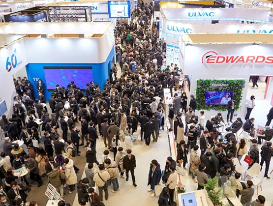
At SEMICON West 2020, the Honorable Al Gore, former U.S. Vice President and recipient of the Nobel Peace Prize for environmental activism, commented on the world being in the midst of a “sustainability revolution.” Just what did he mean by that, and why bring that message to us? The answer is that he believes the digital transformation wields the magnitude of the agricultural and industrial revolutions, but with the exponential speed that the semiconductor industry created and enabled. Ok, that would put him in the right place… SEMICON West.Among a rich lineup of speakers to mark the 50th anniversary of the event – and 50 years of the semiconductor industry facilitating the innovation of the Information Age -- Gore joined other icons in their fields who graced the virtual stage for our featured keynotes. Each analyzed how microchip advances are critical to solving some of the world’s greatest challenges.As host of the conference, I had the privilege of introducing Gore; Gary Dickerson, President and CEO of Applied Materials; and, Dr. John Kelly III, Executive Vice President and Director of IBM Research, along with other renowned speakers. Their insights seemed especially timely for how our global supply chain can help to build a more sustainable future. Following are a few of the highlights from their discussions. Al Gore – The Planet Faces Existential CrisisIn his keynote conversation with Greenbiz editorial director Heather Clancy kicking off SEMICON West 2020, Gore emphasized that digital technology advances – and in particular microchip innovation – provide the greatest opportunities to overcome the world’s most epic challenges. Chip breakthroughs will be the cutting edge of what he called the rapidly growing sustainability revolution to improve energy efficiency, reduce our reliance on fossil fuels, and optimize the performance of renewable energy generated by solar, wind, and electric battery sources.“We face an inflection point as we rely more on data and communications technology, particularly in areas like cloud computing and artificial intelligence,” Gore said. “Industry is aware of this and working on it, but this meeting (SEMICON West 2020) with your present leadership marks a real turning point. It’s something to be proud of, something to be celebrated. It’s what gives me hope.”Citing Moore’s Law and enormous strides made in chip efficiency and effectiveness, Gore said that within two years smart chips will make everything from solar panels and batteries to renewable energy plants and electric vehicles to be both cost- and performance-competitive with traditional energy sources. Afterwards, renewable energy will be more attractive. Gore urged the energy-intensive semiconductor industry to shift to more renewable power sources for manufacturing. To meet this challenge, Gore encouraged the industry to embrace strategies for “step changes”: First, collaborate and share best practices more transparently across the entire microelectronics value chain. Examples already abound where “cutting-edge apps, AI, and deep learning reduced data server energy use significantly without hardware changes,” he said. Second, reduce electricity required to manufacture smarter and smaller semiconductors. Gore encouraged “all of the equipment manufacturers to work together to reduce the amount of carbon dioxide emissions in manufacturing these advanced semiconductors.” Third, follow the lead of a growing number of companies that “continue decarbonizing the power supply on which data centers operate,” he said. Fourth, work with government through the Science Based Target Initiative, which sets decarbonization limits that keep global temperatures no more than two degrees Celsius above preindustrial levels. Finally, rely on “diversity of thought” and “collective thinking” when innovating for the digital future. Research and experience prove that different points of view lead to better decisions. The technology industry has made progress in workforce diversity, but more can be done, Gore said. This last point plays to our collaborative strengths as SEMI members and an industry. “It is just unbearable to imagine a future generation living with the kinds of consequences scientists tell us would ensue if we don’t heed their warnings and solve this crisis,” Gore said, drawing parallels to the COVID-19 pandemic. “We have to accept the situation and make sure we do everything we can. I am inspired by this industry’s leadership, innovation, and spirit to rise to the challenge and make a difference.”Gary Dickerson – Making Possible A Better FutureTo ensure another 50 years of accelerating growth and innovation, today’s semiconductor leaders must share a deep commitment to a more sustainable and just supply chain industrywide.“The first thing we need to do is decouple our growth from environmental impacts,” Dickerson said in his keynote. “Our responsibility as leaders is to leave the world a better place.”Dickerson said that while he firmly believes the explosion of processing and storage data has “the potential to change the world,” the downside is that it also has the potential to rapidly expand our industry’s carbon footprint. Without dramatic change, electrical usage will continue to rise as machines generate and consume more data, compute performance progresses, and workloads from the edge to the cloud grow.“It will be impossible to create neural networks (using AI) with the rate of today’s power consumption,” Dickerson said, noting that more improvements must be made in the performance and efficiency of semiconductor devices, architectures, structures, materials, and advanced packaging.Dickerson urged the electronics ecosystem to “permanently think and act differently” by breaking down communication barriers among systems integrators, equipment suppliers, design and manufacturing service providers, and other industry players. Sharing learnings and best practices will be vital to this change, he said. Dickerson unveiled SuCCESS2030 (Supply Chain Certification for Environmental and Social Sustainability) – Applied Materials’ 10-year roadmap for creating a more sustainable supply chain – during his talk. Under the SuCCESS2030 initiative, Applied Materials will hold its suppliers to the company’s own high standards for committing to renewable energy and workforce diversity by setting targets such as: Reducing supply chain carbon emissions 15 percent in four years by relying more on intermodal shipping than air freight Transitioning the supply chain to recycled content packaging, with a target of 80 percent by the end of 2023 Eliminating phosphate-based, pre-treatment of metal surfaces by 2024 Working with trade associations like SEMI to develop diversity and inclusion strategies to increase underrepresented minorities in the workplace Dickerson said that deeper and more open partnerships between Applied Materials and its customers and suppliers have led to a number of promising outcomes. Examples include hardware and software upgrades, product and service optimizations, and improvements in chip architectures that increased throughput density for higher system performance while decreasing power and chemical consumption, costs, and space requirements. What’s more, Applied Materials recently introduced its Selective Tungsten Process Technology, which uses new materials, atomic-level designs, and ultra-clean rooms to improve the performance of interconnected transistors while lowering power consumption.Dickerson said the COVID-19 pandemic has awakened the world to the power of digital technologies that make it possible to communicate, collaborate, and share data across the globe while sheltering in place. “When I think of the world’s grand challenges, it’s clear the semiconductor industry has a critical role to play,” Dickerson said. “I strongly believe we’re in a position to shape the future and leave the world a better place.”John E. Kelly III – 50 Years That Changed The World … And We’re Just Getting Started During the past half century, semiconductors have given rise to essentially every major technology advance, Kelly said in his keynote. Microchip innovation has played a central role in rocketing humans to the moon, simulating nuclear weapons on a supercomputer, connecting people to nearly everything via mobile devices, and keeping people alive with pacemakers and other electronic medical devices.The strides in innovation have been staggering. In 1970, a semiconductor chip featured a few thousand components. Today, that number stands at 50 billion. Breakthroughs in everything from materials and chemicals to polishing, processes and interconnectivity have driven gains in power-efficiency and performance while reducing chip size.Moore’s Law is far from dead. Paraphrasing Winston Churchill, Kelly said, semiconductor innovation today is not at “the beginning of the end, but at the end of the beginning, and the best is yet to come – driven by extreme collaboration and extreme innovation to solve the world’s biggest challenges.”Kelly said he believes technology is the only answer to the onslaught of grand challenges confronting societies and people today, including air and water pollution, climate change, diminishing natural resources, storm-related disasters, food supply shortages, and the COVID-19 pandemic.Kelly lamented that the world’s response to COVID-19 illustrates that “not much has changed” since the Spanish Flu crisis a century ago. The same technology – masks – remains the primary defense. “I think if we had used digital technologies and computer modeling earlier on, we could have detected the spread of this flu” to minimize its impact, Kelly said.Today’s computer modeling and analytics capabilities aren’t quite ready yet to tackle such complex problems as pandemics, global warming, or water contamination. However, Kelly said, several game-changing technologies – all powered by semiconductors – are emerging as promising answers to our most daunting challenges.“It’s all about the data, and artificial intelligence is the way forward – it’s analytics on steroids, and many new devices will be required to drive AI at the scale of these problems,” Kelly said. “The second technology revolves around not just cloud computing but edge computing and cloud at the edge. Data will be generated in enormous amounts at the edge, which is where we will need to store and compute the data. The next is Quantum Computing. Frankly, we do not have enough computing power yet to look at some of the biggest challenges we have.”All these advances will present new challenges for the semiconductor industry, such as developing new materials, new chip architectures and new mapping structures for AI-embedded devices to reach their full potential.With many of these disruptive innovations too large for any company to solve singlehandedly, Kelly advised industry players to form more “radical partnerships.”“Extreme collaboration and extreme innovation will drive solutions to all these world challenges,” Kelly said. “The best is yet to come.”Radical partnerships… Sustainable revolutions… Extreme innovation… It’s been 50 years of SEMICON West, but it sounds like we’re just getting the real magic started. Like John Kelly said and the other keynoters emphasized, the best is yet to come.Dave Anderson is president of SEMI Americas.
Read More
Emerging applications powered by 5G and artificial intelligence (AI) are expected to be a boon to the semiconductor industry, but only once chipmakers overcome a key challenge: Architecting chips that meet the exacting performance, power consumption, size and cost requirements of devices for mid- to high-end applications. One technology – heterogeneous integration – promises to meet these demands and help drive future leaps in semiconductor innovation in the post-Moore era. To help the industry better grasp the technology challenges and business opportunities associated with deploying highly integrated chip and packaging technologies, SEMI and AI on Chip Taiwan Alliance recently gathered industry leaders from organizations including ASE, Unimicron, Dialog Semiconductor, Cadence and AITA to discuss technology trends and the vital importance of building a cross-industry exchange platform to advance next-generation manufacturing processes critical to heterogeneous integration. Following are key takeaways from the forum, Heterogeneous Integration Enables 5G and AI. Overcoming Heterogeneous Integration Technology Challenges Key to Advances in Taiwan High-End Semiconductor Manufacturing The introduction of the Heterogeneous Integration Roadmap (HIR) by the International Technology Roadmap for Semiconductors team in 2016 was an important first step, Dr. C.P. Hung, Vice President of ASE Group, noted in his opening remarks. The HIR is designed to stimulate pre-competitive collaboration to advance heterogeneous integration technology development and accelerate electronics innovation. The roadmap provides a long-term vision for the electronics industry, identifying future technology requirements and potential solutions. Today, the HIR working group focuses on high-performance computing (HPC), 5G and other leading-edge technologies.Dr. Hung predicted that heterogenous integration will reshape traditional collaborations between the semiconductor ecosystem and supply chain in order to clear I/O bottlenecks that hamstring high-performance applications. The retooled industry connections will also need to enable high I/O pin counts, ultra-thin devices, and high-frequency signal shields. In an important step forward, the chip industry today is developing a platform that enhances wafer-level advanced packaging services and deepens cooperation with Oversea Assembly and Testing (OSAT) and substrate supply chain partners. Overcoming the current limits of IC substrates – the connection between IC chips the PCB – is one key for heterogeneous integration technology to flourish, said Dr. Yu-Hua Chen, Vice President, Carrier SBU, RD Division of Unimicron. He noted that the industry must tackle limits to PCB thickness, substrate density, fine pitch and automation to meet the needs of high-end packaging customers. Another barrier the industry must be surmounted is to make the currently inscrutable confidentiality requirements for patents of foreign materials – key to improving chip yields – easier to access and understand for substrate engineers. Chen said partnerships across the entire industry will be necessary to break through this and other technology breakthroughs. Supply Chain and Cross-Border Ecosystem to Strengthen Partnerships for Further DevelopmentTaiwan has long invested heavily in advancing semiconductor manufacturing and application engineering technologies to become a top global chipmaking hub and, in the process, has been behind significant leaps in optimizing chip functionality, said Leroy Liu, General Manager, Asia Headquarters, of Dialog Semiconductor (Germany). With its semiconductor manufacturing prowess, Taiwan can also play a central role in maturing advanced heterogeneous integration packaging technology while managing development costs by partnering with its international supply chain community to overcome technical challenges more effectively, Liu said. The region can also help forge partnerships, even among competitors, to build the ecosystem essential for heterogeneous integration technology to shine.EDA tools will be critical in understanding and resolving heterogeneous integration technical issues since IC substrate, packaging and chip design all pose interdisciplinary engineering challenges, said Julian Sun, Product Marketing Director at Cadence. To help the industry navigate these challenges, Cadence has launched intelligent system design products – solutions that address a wide range of design problems with semiconductor nanometers, micrometers on packaging and testing, and PCB level micro/millimeters to Pin/Pitch, I/O models, and thermals and electricity. By supporting various technical designs, Cadence helps customers shorten the design cycle to strengthen design quality and reduce costs.Sun also pointed to the vital importance of overcoming the significant challenge of designing silicon interposers for heterogeneous integration. Today’s EDA tools are capable of optimizing the design of complex structures including 5GAiP and HBM and are instrumental in aiding Taiwan’s semiconductor ecosystem players to quickly adapt to shifts in the evolving heterogeneous integration market.Heterogeneous Integration Enables 5G and AI speakers (L-R): Julian Sun, Product Marketing Director at Cadence, Dr. Yu-Hua Chen, Vice President, Carrier SBU, RD Division of Unimicron, Dr. C.P. Hung, Vice President of ASE Group, Leroy Liu, General Manager, Asia Headquarters, of Dialog Semiconductor (Germany), Dr. Shih-Chieh Chang, AITA Executive Secretary Designing AI chips is particularly difficult as semiconductor makers struggle with high costs and low yields, said Dr. Shih-Chieh Chang, AITA’s Executive Secretary. That’s why the chip industry now uses FPGAs for small-volume production of AI chips, which makes it easier to improve manufacturing yield through redundant design. For its part, AITA has formed a special interest group (SIG) to help form connections among the chip industry, academia and research institutes. The association’s goal is to build a platform for mass production of AI chips.To get involved in SEMI Taiwan Heterogeneous Integration related events, please contact Ula Huang, outreach senior specialist, at [email protected] Fang is a coordinator and Ashley Huang is a specialist in marketing and public relations at SEMI Taiwan.
Read More
During the COVID-19 pandemic, the SEMI Global Advocacy team has been working tirelessly to ensure the microelectronics manufacturing and design supply chain is classified as an “essential business” in the United States and for similar designations in several other countries so that SEMI member companies can maintain operations. Their efforts have included direct lobbying and letters to the governors of 16 states in the U.S., 23 European countries and several European Union officials across the continent, as well as government officials in Japan, Mexico and Malaysia. The bedrock of these efforts, and the reason they have been highly effective, is that our industry enables both modern digital infrastructure and technology critical in the fight against the virus.SEMI takes immense pride in highlighting the role of our industry in providing the building blocks for innovations that improve social and economic prosperity the world over. It is never more apparent that necessity is the mother of invention than during a crisis, and the pandemic has created a diverse range of demands for technological advancements to address the myriad of challenges it presents. Our SEMI Tech Spotlight blog series highlights some of the many ways that our industry and member companies are enabling technology employed on the front lines of this fight – and that we strongly believe will ultimately help to win it. Our first piece in this series focuses on platforms enabled by big data and artificial intelligence.Fighting the Pandemic with Big Data-AI Enabled PlatformsThe COVID-19 pandemic is testing humanity in unprecedented ways, but it is also uniting us to fight this crisis with the best weapons we have. Big data and Artificial Intelligence (AI) technologies – built with microelectronic chips and systems that generate, transmit, store and analyze data – are making a profound contribution to our arsenal for this protracted war. Big data-AI technologies are enabling platforms such as data analytics, robotics, augmented/virtual reality (AR/VR), 3D printing, and others that are already being applied to address many facets of this crisis.Big Data and Analytics Inform Policy In the fight against COVID-19, data analytics platforms are being used first and foremost to slow the rapid spread and to inform policy decisions. This requires analysis of massive amounts of data about public health and travel, often using AI algorithms. The state of California, for example, is partnering with companies such as BlueDot, Esri and Facebook to build a software platform that uses smartphones and location intelligence to track people’s movement and predict hospital needs. Taiwan owes its considerable success in limiting the spread of the virus to the extensive use of big data analytics for identifying and tracking carriers. Google and Apple are driving a joint effort that connects Bluetooth with their popular iOS and Android platforms to trace contacts of infected people. India has developed Aarogya Setu, a mobile app based on Bluetooth and location-mapping platforms, designed to alert citizens if they have crossed paths with another app user who has tested positive for the virus. This app was launched in 11 languages, and despite being entirely voluntary, it was downloaded by 50 million people in 13 days, making it the world’s fastest-ever to reach that number. Such contact-tracing apps, now being rolled out in at least 26 countries, carry inherent privacy and security challenges due to the sensitive data they access. While mitigation strategies like strict data anonymity and opt-in protocols are being implemented, these will need to be refined over time.Robotics Protect Frontline SoldiersToday’s robust robotics platforms are enabled by huge amounts of data from sensors and guidance from predictive AI algorithms. These robots can learn on the job, adapt to the environment, and work safely with humans. In this pandemic, they are perfect for minimizing human interaction with infectious environments. Companies around the world such as Boston Dynamics, Akara Robotics, UBTECH Robotics and CloudMinds have already deployed robots on the front lines of this war to assess patient health, disinfect hospital surfaces, and help health workers with Personal Protective Equipment (PPE).Robot drones are also delivering blood and other lab samples. For example, WakeMed hospitals in North Carolina launched the first drone delivery program approved by the U.S. Federal Aviation Administration with Matternet drones operated by UPS; while Terra Drone from Japan executed similar tasks in the hard-hit Wuhan province of China.3D Printing Speeds ManufacturingBig data-AI technologies enable 3D printing platforms by providing accurate 3D models for optimized designs and defect-free manufacturing. Low-cost, fast-cycle-time 3D printing has helped to alleviate at least some of the medical equipment shortages. For example, the U.S. Food and Drug Administration (FDA) has approved the first 3D-printed “Stopgap Face Mask” for liquid barrier protection from the SARS-CoV-2 coronavirus for healthcare workers. The U.S. Veterans Health Administration has developed this in collaboration with America Makes using an open-source database – the 3D Print Exchange from the National Institutes of Health. In another example, Formlabs worked with Northwell Health, New York’s largest healthcare provider, and University of South Florida (USF) Health to develop and test a nasal swab prototype over just one weekend, and it is now producing up to 150,000 test swabs daily. Prisma Health in South Carolina received emergency FDA authorization for VESper, a 3D printed device that allows a single ventilator to support two patients, and possibly up to four.Telehealth Becomes a “New Normal”Telehealth is not a new concept but is much enhanced by today’s microelectronics platforms that can collect and transmit rich datasets with very low latency. Further, rapid data analysis is increasingly supported by AI systems. The requirement for social distancing makes telehealth a perfect solution for many healthcare consultations. U.S. government data indicates that the daily average of telehealth claims from private insurance for upper respiratory infections increased nearly 12 times over the previous month from March 14 to April 1. Similarly, Teladoc Health coordinated 100,000 patient “televisits” in the week of March 8 – a 50 percent spike over the previous week, taking pressure off the healthcare system. The next generation of telehealth is likely to use AR/VR platforms, which use even richer datasets and AI to improve the accuracy and predictive capability of their underlying models. Consequently, these platforms can provide more realistic experiences and improved outcomes. At least 11 states in the U.S. are already working with AR/VR companies such as XRHealth and AppliedVR for primary care and many medical specialties. Accelerating the Search for a Vaccine or TreatmentThe way out of this pandemic depends on swiftly finding a vaccine and a treatment, ideally by fast-tracking the traditionally slow drug development process. Big data-AI technologies are at the forefront of such efforts globally, often using the most powerful supercomputers available. For example, researchers at the University of California, San Diego (UCSD) are using the Frontera supercomputer to build a complete model of the SARS-CoV-2 coronavirus envelope – a formidable task, requiring analysis of data from 200 million atoms and interactions between them. Researchers at Argonne National Laboratory are combining AI with physics-based models to search for a molecule that might disrupt the activity of the virus, a precursor to finding a treatment. Also, several companies around the globe such as BenevolentAI (UK), Gero (Singapore), Innoplexus (Germany-India), and Insilico Medicine (US-Hong Kong) are using AI platforms to accelerate the search for a solution. ConclusionUltimately, the success of technology is not measured by the number of bits and bytes or by the speed of algorithms. It is measured by every janitor who did not have to clean a hazardous surface because a robot did, by every doctor and nurse protected by a 3D-printed mask, and by every person whose life may be saved by the accelerated discovery of a vaccine or treatment. Big data-AI technologies, and the platforms they enable, are just coming of age – they give us hope that as they evolve in the future, we can use them to build a more resilient society and economy.Note/Disclaimer: The examples cited above are purely for illustration – they are neither comprehensive, nor intended to endorse any particular product or solution.The SEMI Smart Data AI initiative helps members realize full value in the intelligent future enabled by Big Data and Artificial Intelligence – including the large revenue upside, and the transformational potential for operational and supply-chain efficiency. For more information on the initiative, contact Pushkar Apte at [email protected] Manocha is President and CEO of SEMI. Pushkar P. Apte, Ph.D., is the Strategic Technology Advisor for the Smart Data AI Initiative at SEMI.
Read More
Smart technologies have gripped the world’s imagination with their promise to revolutionize the way we live and work. With the semiconductor supply chain central to these advances, SEMI Japan in October hosted 200 members for SEMI Japan Members Day as speakers from three of the world’s top device manufacturers – Denso, Sony and Kioxia – offered their perspectives on the strides the semiconductor industry needs to make in three key areas: automotive, smart manufacturing and 3D flash memory manufacturing technology. Automotive Evolution and Electronics – DensoThe automotive industry is re-inventing itself to innovate across connectivity, autonomy, sharing and electric (CASE) and ensure safe, comfortable and environmentally friendly autonomous driving, said Nobuaki Kawahara, executive fellow and director of the Advanced Research and Innovation Center at Denso. Key focus areas of Denso in CASE innovation are Extraordinary Safety and Everyday Confidence. The company’s goal is to minimize damage to vehicles involved in collisions or one-car accidents by making it easier for drivers to detect and steer clear of objects in their path.To improve automobile safety and security, the company is developing advanced driver-assistance systems (ADAS) and autonomous driving technologies as it promotes the confluence of four areas of technology – HMI (Human Machine Interface), environmental recognition, vehicle control assistance, and information and communications. One use case Denso sees as a significant opportunity is deploying sensors such as millimeter-wave radar, cameras and LiDAR to monitor a vehicle’s surroundings, using GPS and precision mapping to pinpoint its location and determine the best route for safety and distance, and then transmitting that information to a motion-control system.Denso is also out to solve the hard challenges associated with autonomous driving in dynamic road conditions. Kawahara pointed out that road conditions vary and that rules for "driving at certain intervals in a certain lane" vary depending on the time of day. Also, on public roads in Abashiri, Hokkaido, where the company is currently conducting field tests, snowfall makes it difficult to recognize road images and gather sensor information. In Asia, it is also common for motorcycles and automobiles to speed along with very little space between them.Image Sensors to Accelerate Development of Smart Manufacturing – SonyTo fulfill the promise of smart manufacturing, the semiconductor supply chain must continue to invest in sensor and imaging technology innovation, said Shigeo Ohba, deputy senior general manager of the Imaging System Business Division at Sony Semiconductor Solutions. For its part, Sony is developing imaging sensors that help network and automate factories to achieve new production and cost efficiencies. For example, the company plans to design devices to increase equipment uptime through predictive maintenance, reduce defect rates and drive other manufacturing efficiencies. The challenge with today’s factory lines that produce a number of different devices is that they are highly complex to manage and therefore prone to human error, undercutting manufacturing efficiency. In the future, AI-powered machines will leverage data analysis to help streamline operations. Adapting an image sensor with AI to machine vision applications can simplify key processes such as measurement and inspection processes while reducing safety and security costs.Of the vast amount of information on all machines connected to the cloud, only essential details will be processed at the edge since edge data processing offers stronger security and reduces data transfer time. Ohba said image sensors will evolve based on edge AI, adding that "AI will be a paradigm shift for image sensors if it’s economically feasible."3D Flash Memory Manufacturing Technology Challenges – KioxiaIncreasing connectivity in factories for smarter, more efficient operations places huge demands on memory since networked devices typically store duplicate data, said Hideshi Miyajima, head of the Advanced Memory Development Center (AMDC) at Kioxia. To meet demand for higher networking speed and capacity, 2d NAND flash memory is moving to 3D and, in particular, three 3D techniques: multivalued memory, cell partitioning and layer stacking.To increase storage capacity, the third-generation 64-layer BiCS FLASH™ stacks layers to form nearly two trillion holes with a diameter of 100nm and a depth of 5μm on a wafer and places a uniform 2-3nm thin film on the inner wall of each 5-μm hole. For its BiCS FLASH™, Kioxia uses a dry etching technique that forms a straight, elongated through-hole and atomic layer deposition (ALD) technology, which creates a uniform laminate atomic layer on the wafer surface to grow materials uniformly and with high precision on large, complex substrates.In order to meet the cost expectations of high-volume 3D flash memory manufacturers, outlays across fabs must be reduced by better monitoring plasma control, enhancing yield through particle control, speeding film formation, and reducing gas, power and water usage, Miyajima said.SMART Transportation and SMART Manufacturing in the Spotlight at SEMICON JapanPlease join us at SEMICON Japan 2019, December 11-13 at Tokyo Big Sight, for the latest developments and trends in SMART Transportation and Smart Manufacturing. There are also a few other great reasons to attend. We look forward to seeing you in Tokyo!Jim Hamajima is president of SEMI Japan.
Read More
As a top semiconductor manufacturing hub, Korea is poised to lead the world in fab construction spending in 2019 and 2020, accounting for 27 percent of the total market. Little wonder that Korea’s prowess in the semiconductor industry has meant steady membership growth for SEMI Korea, with HD Cho, president of SEMI Korea, putting the average annual jump at about 7 percent.But HD Cho’s focus as he returned to COEX in Seoul, home to SEMICON Korea, in late August was not on membership growth over the years but the future. Cho hosted about 400 SEMI members gathered at SEMI Korea Members Day for insights into the state of the world economy, semiconductor industry outlooks, and perspectives on how South Korean and European microelectronics companies can form stronger ties. Setting the stage with look at macroeconomics, Byung-yeon Kim, team manager of NH Investment and Securities, predicted that, as the global economy continues to falter, 25 of the 58 major countries this year will cut interest rates in a bid to boost prospects for growth. Historically, the global composite leading indicator (CLI), a bellwether for turning points in the economy, has rebounded after 20 months of decline, he said. While the CLI downtrend is now past the 20-month mark, Kim struck a bullish note, predicting that the global economy will bounce back before long.Soo-kyoum Kim, vice president at IDC, referring to the semiconductor industry’s own soft patch, said that total revenue is expected to drop from $475 billion in 2018 to $440 billion this year but should rebound to a new high of $500 billion in 2023. The memory market will be especially hard-hit, dropping more than 29 percent in 2019 and another 14 percent next year before bottoming and then staging a recovery in the second half of 2020. The strength of the rebound will hinge on server market demand, he added.Next year will also see rebounds in semiconductor equipment and materials revenue, with growth of 12 percent and 3 percent, respectively, said Clark Tseng, director of Industry Research and Statistics at SEMI. The increases will follow a 2019 equipment market drop of 18 percent to $53 billion from the previous year while materials this year is expected to remain flat at $52 billion. The semiconductor industry will expand at a modest 2.4 percent this year, jumping to 7.6 percent in 2020, Tseng reported, citing the average growth rate based on data from Gartner, WSTC, IC Insights, VLSI Research and other industry analyst firms. Despite current weak market demand and the ongoing trade war, the long-term outlook for the semiconductor industry remains upbeat, he added.In Europe, semiconductor industry growth continues on the strength of the region’s high strategic importance in the global electronics supply chain, said Laith Altimime, president of SEMI Europe. Fab construction spending in Europe continued to grow in 2018, reaching $300 million, and is expected to hit $1.2 billion in 2019 and $1.6 billion in 2020, with equipment, parts and components driving the surges.To help build stronger ties between European and Korean chip industries, Altimime introduced the SEMI Korea members to SEMI Europe business platforms including SEMICON Europe, the 3D System Summit, ISS Europe, and the MEMS Imaging Sensor Summit. He also encouraged the formation of more business partnerships between companies in the two regions by familiarizing SEMI Korea members with European players in areas such as foundry, MEMS, sensors and wafer manufacturing.And it will be MEMS and sensors that help drive the 4th Industrial Revolution, said Sung-hyuk Kim, a team leader at LG Electronics' Sensor Solution Research Institute. In his presentation Architecting Sensor Solutions for the Next Revolution, he noted that sensors are finding their way into devices where they have never been used before. In household refrigerators, gas sensors help deodorize the inside while distance sensors detect the approach of people. Air conditioners equipped with a camera sensor can pinpoint the location of humans and steer the airflow in their direction. Of course, all these smarts will come in form of data-devouring artificial intelligence (AI), and that data will be generated in massive amounts by MEMS and sensors – placing them at the epicenter of the 4th Industrial Revolution.Jaegwan Shim is a marketing specialist at SEMI Korea.
Read More
In the long unfolding arc of technology innovation, artificial intelligence (AI) looms immense. In its quest to mimic human behavior, the technology touches energy, agriculture, manufacturing, logistics, healthcare, construction, transportation and nearly every other imaginable industry – a defining role that promises to fast track the fourth Industrial Revolution. And if the industry oracles have it right, AI growth will be nothing shy of explosive.“The gains these days are not incremental,” said Ajit Manocha, SEMI president and CEO, said to a gathering in July of the Chinese American Semiconductor Professional Association (CASPA) for its Summer Symposium at SEMI’s headquarters in Milpitas. “They are hockey stick – exponential – with AI semiconductors growing in market size from $4 billion this year to $70 billion in 2025.”Manocha left little doubt that AI is remaking the semiconductor industry and, in the process, the world at large. Internet of Things (IoT) and 4G/5G, both key AI enablers, will account for more than 75 percent of device connections by 2025.“Today, 30 billion devices worldwide are connected,” Manocha said, citing an Applied Materials prediction that the number of connected devices globally will grow to between 500 billion and 1 trillion by 2030. Those devices will generate stunning amounts of data collected, interpreted and used to reason, solve problems, learn and plan, leading to the holy grail of autonomous machine behavior.To process this colossal amount of data central to the promise of AI, the industry must break through the limits of a key technology: memory. Memory a Critical AI BottleneckThe challenge for memory starts with performance. Historically, every decade gains in compute performance have outpaced improvements in memory speed by 100 times, and over the past 20 years that gap has grown, said Steven Woo, a fellow and distinguished inventor at Rambus, presenting at the symposium. The upshot is that memory has bottlenecked compute and, in turn, AI performance. The industry has responded with new ways to implement memory systems on AI chips. Each is suited to unique performance requirements and, of course, comes with trade-offs. Among the frontrunners: On-chip memory delivers the highest bandwidth and power efficiency but is limited in capacity. HBM (High Bandwidth Memory) offers both very high memory bandwidth and density. GDDR balances trade-offs among bandwidth, power efficiency, cost and reliability. Since 2012, AI training capability has grown 300,000 times, besting Moore’s law by 25,000 times in doubling every 3.5 months, a blistering pace compared to the 18-month doubling cycle of Moore’s law, Woo said. The staggering improvements have been driven by parallel computing capacity and new application-specific silicon like Google’s Tensor Processing Unit (TPU).These specialized silicon architectures and parallel engines are key to sustaining future gains in compute performance and combatting the slowing of Moore’s Law and the end of power scaling, Woo said. By rethinking the way processors are architected for certain markets, chipmakers can develop dedicated hardware capable of operating with 100 to 1,000 times greater energy efficiency than general purpose processors to overcome another big limiter to scaling compute performance – power.For its part, the memory industry can improve performance by signaling at higher data rates and using stacked architectures like HBM for greater power efficiency and performance, and by bringing compute closer to the data.Memory scaling for AIA key challenge is scaling memory for AI. Demand for better voice, gesture and facial recognition experiences and more immersive virtual reality and augmented reality interactions is tremendous, said Bill En, senior director at AMD, speaking at the symposium. These capabilities require more processing power across both high-performance computing (HPC) for big data analytics and machine learning as it relies on AI and machine intelligence to generate meaningful insights. Emerging machine learning applications include classification and security, medicine, advanced driver assistance, human-aided design, real-time analytics and industrial automation. And with 75 billion IoT-connected devices – all generating data – expected by 2025, there will be no shortage of data to analyze, En said. The wings alone of a new Airbus A380-1000 feature some 10,000 sensors.Mountains of this data are stored in massive data centers on magnetic hard drives, then transferred to DRAM before moving to SRAM within the CPU for the handoff to the compute hardware for analysis.With data growing at an exponential clip, the question is how to make sure all other memory systems can handle the flood of data. AMD’s answer is a chiplet architecture featuring eight smaller chips around the edge that drive the compute and a large chip in the center that doubles the IO interface and memory capability to in turn double chip bandwidth.AMD has also moved from a legacy GDDR5 memory chip configuration to HBM to bring memory bandwidth closer to the GPU for more efficient processing of AI applications. The HBM provides much higher bandwidth while reducing power consumption. Compared to DRAM, AMD’s HBM delivers a much faster data rate and far greater memory density, En said.Over the next decade, look for more performance improvements from multi-chip architectures, innovations in memory technology and integration, aggressive 3D stacking and streamlined system-level interconnects, he said. The industry will also continue to drive performance gains in devices, compute density and power through technology scaling.Michael Hall is a global marketing communications manager at SEMI.
Read More
Technologies promising huge growth such as Artificial intelligence (AI), 5G, machine learning, high-performance computing, and telematics are ratcheting up pressure on semiconductor manufacturers in the race among product makers to accelerate time to market and capture share. To support rapidly evolving end markets for these and other technologies that are key drivers of industry growth, chipmakers are boosting semiconductor performance, producing more wafer sizes and improving manufacturing efficiency.At the same time, chip manufacturers must enable unprecedented end-product reliability for exploding markets such as automotive and healthcare markets where, with lives at stake, products can’t afford even the slightest lapse in reliability. In response, chip suppliers are retooling their manufacturing processes to support 3D stacking, package-level integration and miniaturization. But they must do more. Bringing high efficiency to all phases of manufacturing including design and materials is the new imperative. The key to quality management is not in the traditional post-production testing and damage control but in prevention. Delivering the highest quality and reliability must start in the earliest stages of production with manufacturing and testing design – an approach that reduces not only the cost of downstream testing but minimizes product defects that can damage a supplier’s credibility and lead to lost business.To that end, SEMI has launched its Quality Assurance Special Interest Group (SIG) consisting of representatives from industry leaders such as Infineon, NXP, TSMC, UMC, ASE, Unimicron, and GCE. The group's goal is to establish quality requirements spanning the supply chain to meet new, higher reliability standards and help safeguard Taiwan’s competitive edge in the global microelectronics industry. Meeting for the first time earlier this month, the companies exchanged ideas for improving quality management in semiconductor manufacturing and ultimately deliver the reliability the market needs.The company representatives unanimously agreed that the first step is to ensure a QA-friendly environment with quality requirements for various stages of chipmaking ranging from design, manufacturing, packaging and testing to even PCB and CCL production. The SEMI Quality Assurance SIG this year plans to build on its current membership by enlisting companies from various fields to address critical areas of reliability including statistical process control, surface-mount-technology-based board level reliability control, and 0 dppm quality control for automotive chips. SEMI Quality Assurance Special Interest Group consists of leading companies in the industry, including Infineon, NXP, TSMC, UMC, ASE, Unimicron, and GCE. “SEMI’s comprehensive platform of exhibitions, programs, forums, trade meetings and matchmaking events is instrumental in bringing together key industry players to enhance quality management practices and meet the growing reliability requirements of the end markets we serve,” said Terry Tsao, chief marketing officer at SEMI and president of SEMI Taiwan. “The Quality Assurance Special Interest Group is a shining example of how SEMI continues to support the crucial role of Taiwan’s semiconductor industry in the international community.”For more information about the SEMI Quality Assurance Special Interest Group or to become a member, please contact Emmy Yi at [email protected] Yi is a marketing specialist at SEMI Taiwan.
Read More