downloadGroupGroupnoun_press release_995423_000000 copyGroupnoun_Feed_96767_000000Group 19noun_pictures_1817522_000000Member company iconResource item iconStore item iconGroup 19Group 19noun_Photo_2085192_000000 Copynoun_presentation_2096081_000000Group 19Group Copy 7noun_webinar_692730_000000Path
Skip to main content
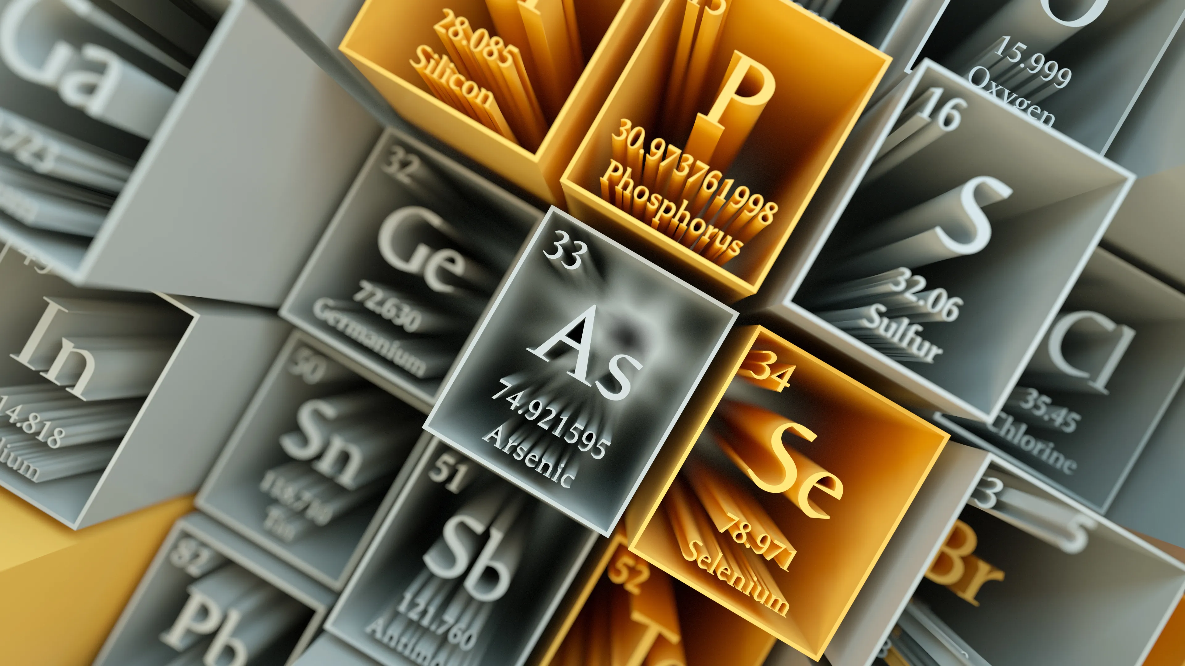
Most of today’s blockbuster MEMS products – from pressure sensors and resonators to accelerometers and microphones – originated from academic research, a trend that Alissa M. Fitzgerald, Founder Managing Member, A.M. Fitzgerald Associates, expects to continue. While many of these potentially game-changing new technologies will require many more years of intensive development and up to $100 million in investment to reach full commercialization, Fitzgerald sees their potential for generating new waves of activity and opportunity in the MEMS and sensors industry.SEMI’s Maria Vetrano caught up with Fitzgerald to preview her October 23 presentation, Emerging MEMS Sensors Technologies to Watch as We Enter a New Decade, at MEMS Sensors Executive Congress, October 22-24, 2019, at the Coronado Island Marriott Resort Spa in Coronado, California.Join us at MEMS Sensors Executive Congress (MSEC) to meet Alissa Fitzgerald and other industry influencers driving innovation in the MEMS and sensors industry. Register now to connect with her at MSEC or visit her on LinkedIn.SEMI: What are your top three emerging MEMS and sensors technologies with the greatest promise?Fitzgerald: Let’s start by defining emerging. In researching this topic for MSEC, I reviewed a year’s worth of academic papers to search for compelling technologies that will emerge five to 10 years from now. While these applications are not yet commercially ready, they bear a distinct presence in academic literature, and some have even reached the proof-of-concept phase. They all have the potential to advance user functionality derived from MEMS and sensors in very meaningful ways.Next-Generation MicromirrorsI’ve noticed renewed interest in micromirrors, driven by interest in LiDAR for autonomous vehicles, in fiberoptic networking, and in VR/AR glasses and headsets as well.Newer generations of micromirrors will use piezoelectric films to enhance optical performance. Piezoelectric actuation can pivot the mirror to a much larger angle than older-generation electrostatically actuated micromirrors. This is important for wider-angle scanning for LiDAR – as well as for other applications – as it enables the creation of a larger picture image.Piezoelectric films can also be used to change the shape of the mirror surface to enable a variable-focus mirror. This is useful on two fronts: It supports depth-of-field adjustments and it alleviates the need for extreme precision in packaging of optical devices, improving both cost and yield.Event-driven sensors/zero-power/ultra-low power sensorsSensors that draw no power, or that draw just small amounts, by activating only upon a triggering stimulus, are enormously exciting. Their extremely low power consumption addresses one of the most significant obstacles to creating large-area sensor networks: the problem of too-frequent battery changes.In addition, while most sensor nodes today broadcast a large stream of data back to the mother ship by radio, these event-driven or zero-power sensors consume only a small amount of power because they activate the radio only to transmit essential data.Resolving the power-consumption problem with sensors will allow deployment of large-area sensor networks in remote or inaccessible locations, highly useful for applications such as monitoring infrastructure.Bacterial sensorsSensors that can detect the presence of bacteria, as well as the type, have widespread applicability beyond medical uses. They would be particularly useful in food-safety applications as they can identify particular strains of bacteria, such as E. coli, before the beef leaves the processing plant or the spinach ships from the warehouse. This could offer dramatic improvements in food safety over the Centers for Disease Control (CDC) and U.S. Food and Drug Administration’s (FDA’s) food safety program, which only flags foodborne illness when a cluster of people are seriously ill.Researchers are also designing bacterial sensors for rapid point-of-care (POC) diagnostics to detect, for example, sepsis early, potentially saving lives.SEMI: You’ve said that some future MEMS and sensors will use alternatives to silicon. When might we see MEMS and sensors printed on paper or other flexible materials – and for which applications are they suited?Fitzgerald: We’re seeing an enormous amount of development of sensors made on paper, plastics and even textiles, materials that are readily available, inexpensive and flexible.What’s gating our progress right now is manufacturing infrastructure. At present, researchers are using inkjet printers, 3D printers, etc. to manufacture prototype sensors, but in most cases, they would need to move to roll-to-roll printing to scale up. I think that we’re looking at a decade before we see these sensor technologies reach the mass market.When they do arrive, we’ll see sensors that we can easily affix to any kind of carton, wrapper or packaging used with food or other disposable items. Traceability and status of perishable items in particular will allow consumers to track food from the farm or factory to the warehouse, store and, finally, to the home.Implementing these kinds of sensors would also help the environment. According to the Natural Resources Defense Council, in the United States alone up to 40 percent of our food is wasted annually, in part because we fear it’s gone bad. If consumers feel assured that their food is safe, they will waste less. And wasting less means that we can grow less food to feed the same number of people. We’ll also reduce the volume of food waste that goes to landfills.SEMI: What can the MEMS industry do to promote the use of more environmentally friendly materials in its products?Fitzgerald: Some of this is already underway. More companies in our industry are adopting Restriction of Hazardous Substances (RoHS) standards to get rid of heavy metals, such as lead, cadmium or other hazardous materials, in their electronics.We could also produce disposable sensors on paper or on biodegradable plastics, which would decompose within a few months, and we could use safer metals, such as gold, magnesium or zinc, to reduce hazardous metals’ contamination in landfills. While it’s not feasible to make all sensors biodegradable, the market for such sensors could be massive.As companies (and individuals), we should also work hard to design electronics that consume less power, because this ultimately translates to fewer disposable batteries in landfills.SEMI: What would you like MSEC attendees to take away from your presentation?Fitzgerald: I’d like to make two main points. First, the trend to use other non-silicon materials to make MEMS and sensors is real and inevitable. It’s a matter of when. Anyone building a gas or chemical sensor on silicon should look at how to do it on paper or plastic because there are great future applications incorporating flexible, disposable sensors in packaging of all types. That’s the low-hanging fruit.Second, to support this technology development trend, we must look seriously at manufacturing infrastructure because we will need completely different sets of equipment, environments and consumable materials to manufacture MEMS and sensors on paper or plastic. Sensor manufacturers could prepare for this future expansion by beginning to collaborate today with companies that already produce paper and plastic goods. Alissa Fitzgerald, Ph.D., founded A.M. Fitzgerald Associates, LLC (AMFitzgerald), a MEMS and sensors solutions company, in 2003. She has over 20 years of engineering experience in MEMS design, fabrication and product development.Prior to founding AMFitzgerald, Fitzgerald worked at the Jet Propulsion Laboratory, Orbital Sciences Corporation, Sigpro, and Sensant Corporation, now part of Siemens. She received her bachelor’s and master’s degrees from MIT and her doctorate from Stanford University, in Aeronautics and Astronautics. Fitzgerald has numerous journal publications and holds eight patents. She served on the Governing Council of MEMS Industry Group from 2008-2014 and was inducted into the MIG Hall of Fame in 2013. Fitzgerald serves on the Board of Directors of both Rigetti Computing and the Transducer Research Foundation.For more information, please visit AMFitzgerald.MEMS Sensors Industry Group (MSIG), the industry association representing the global MEMS and sensors supply chain, hosts the annual MEMS Sensors Executive Congress. To learn how MSIG enables professionals in the MEMS and sensors industry to innovate, address common challenges and accelerate business results, visit us today.Maria Vetrano is a PR consultant for MSIG, a SEMI Strategic Association Partner.
Read More
The SOI Consortium’s next annual event in Japan takes place on the 30th and 31st of October in Yokohama. Both days of the SOI Design Symposium will take place in the Yokohama Landmark Tower. The event is complimentary, however pre-registration is required – just follow the link here. Rest assured that in addition to the excellent program, the agenda provides ample time for networking.Wednesday, October 30 -- RF and ULP on SOI: IP ProductsOctober 30th showcases industry leaders with ULP IoT applications by NXP, and opportunities in the RF space by STMicroelectronics and Toshiba. The strong development of the design and EDA platform is discussed by ARM, Silvaco, Attopsemi and Dolphin. GlobalFoundries will present on their predictive reliability platform for RF, while Incize discusses the criticality of RF characterization and Secure-IC addresses to important topic of IC security.The day finishes with an overview of the SOI ecosystem by the SOI Industry Consortium. (See the full agenda here.)Thursday, October 31st -- SOI Enabling Photonics and Power InnovationWe start the day with two keynotes on High Voltage SOI electronics for automotive by NXP followed by Soitec on engineered substrate solutions. The Silvaco overview on RF modeling and SOI NB-IoT by SITRI promises to be very interesting. Then the day will offer a deep dive into Photonics touching applications with Cisco, foundry offerings with TowerJazz and GlobalFoundries, EDA with Cadence, and advanced SOI Photonic solutions by Leti-CEA. An ecosystem and market outlook by Soitec wraps-up the day. (See the full agenda here.)We look forward to seeing you there!
Read More
The ESG MarketElectronic Gases represents the largest percentage of the spend on chemicals and materials by semiconductor producers. Taken altogether, the spend on Electronic Gases was almost $6 billion worldwide in 2018. Recent critical shortages of key gases have impacted the industry tremendously and, in some cases, has also limited output. The Electronic Specialty Gas (ESG) market, while a small segment of the global gas market, is one of the most complex and least understood market segments of the electronic chemicals and materials landscape. Linx Consulting estimates that the ESG market totaled nearly $3.4 billion in 2018, up from roughly $3.1 billion in 2017 with a growth rate of 10 percent last year. Growth was driven by rising demand and the increasing use of higher-value products in applications such as etch and specialized deposition. ESGs are used in the manufacture of electronic devices that are subsequently assembled in systems and in a variety of processes such as film deposition, film etching, substrate doping and chamber cleaning. The devices – semiconductors, LEDs, and displays – are processed on larger substrates, and then separated before assembly.Key differentiators for ESGs are not only the technical complexity of the gases and mixtures supplied, but the purity and consistency demands placed on the gas supply. Product purity and consistency, often at the limits of analytical capability, must go hand in hand with rigorous application of statistical process control in manufacturing and absolute delivery reliability. ESGs include fluorocarbons, hydrocarbons, deposition precursors, dopants, corrosives (halides/hydrates) and rare gas mixtures.The key end-use markets for ESGs include semiconductor wafer fabrication, flat panel display (FPD) manufacture, compound semiconductors / LEDs production and Photovoltaics cell manufacture, as illustrated below in Figure 1. Figure 1 - ESG Market by End-Use Applications Source: Linx Consulting The semiconductor industry is the largest user of ESGs and has the most diverse ESG requirements in terms of products, package sizes and purity requirements. The semiconductor industry uses all the different specialty gases produced. Purities are typically 4N and above and the packages can range from small cylinders to tonner/Y packages to tube trailers. The ESG market is global, with key demand centers in China, Europe, Japan, Korea, Southeast Asia, Taiwan and the United States. The Flat Panel Display (FPD) community is the second largest user group for ESGs. However, the breadth of ESG products used in FPD fabs is much more limited than in the semiconductor industry. Key product applications include silicon sources, dopants, oxidation and nitridation sources, chamber cleans, and etchants. ESG use has grown with the development of the FPD industry across both TFT-LCD segment and AMOLED segment, with many large end users in Korea, China, Taiwan, and Japan. Korea and China boast large ESG supply infrastructures geared towards serving the FPD industry. Early on, these countries targeted the development of the FPD industry and the associated value chain, so there has been large-scale development of required ESG products such as NF3 and silicon precursors. When we review the markets in aggregate, coupled with the geographic intensity of the electronics industry in Asia, it is unsurprising that a vast majority of the ESG market would be in Asia, as illustrated in Figure 2, below.Figure 2 - ESG Market by Key RegionSource: Linx Consulting Key ApplicationsThe applications for ESGs can be readily tied to major thin film fab processes that are commonly used in the microelectronics industry. The processes include dielectric and metal etch, dielectric deposition, metal deposition such as titanium or tungsten, deposition of non-silicon materials such as hard masks etc., dopants for thermal diffusion methods and ion implantation, reactor chamber cleaning; as well as some other specialty applications. This is illustrated in Figure 3 below. Figure 3 - Applications for ESGsSource: Linx Consulting Clearly there is a close tie-in for ESGs into thin film deposition (CVD and chamber cleaning) and etch processing. In the future, the industry will increase its use of ESGs with novel deposition and etch processes. New applications may include lower temperature deposition, high deposition rate processes, flowable CVD films for high aspect ratio structures, and high selectivity deep etching with greater uniformity. All these processes improve device performance and will rely on ESGs and rare gases as enablers. Outlook for ESGsOverall, we believe that the ESG market will grow at a compound rate of about 6 percent over the next five years. Currently the largest six suppliers – Versum Materials, SK Materials, MTG/TNS, Air Liquide, Linde/Praxair, and KDK – control about half of the overall market, with about 50 suppliers accounting for the other half of the market. We anticipate that as the industry continues to grow, we will continue to see changes in the supplier base with both continuing consolidation and new regional suppliers emerging as unique technologies and value-added capabilities enter the market.For More InformationThis article is based on insights and analysis from Linx Consulting’s Electronic Specialty Gas report. The annual report is considered the leading industry source for comprehensive information about demand for specialty gases used in the electronics industry. We track more than 60 different ESG products used across the global semiconductor, flat panel display, solar and compound semiconductor industries.For more information, please contact [email protected], or Mike Corbett at +1 973 698 2331, Mark Thirsk at +617 273 8837, or Andy Tuan + 886 952 111222, or visit Linx Consulting.Interested in engaging with the electronic materials supply chain? The Electronic Materials Group (EMG) is a SEMI technology community representing SEMI member companies that provide substrates, polymers, metals, organic and inorganic materials, chemicals, and gases developed for electronics manufacturing. Linx Consulting has been a longtime member and supporter of the SEMI Electronic Materials Group.Mike Corbett is managing partner and Andy Tuan is managing director, Asia, at Linx Consulting.
Read More
Back in February of this year, we launched SEMI Works™, a landmark SEMI program designed to grow and sustain the electronics industry talent pipeline from the ground up. But it was much more than a program launch. The introduction was a resounding statement of our passionate commitment to workforce development and its incontrovertible importance to the future of the microelectronics industry. No one’s passion for workforce development burns brighter than SEMI CEO Ajit Manocha’s. In April, he reiterated SEMI’s focus to make good on this commitment and laid out the broad outlines of SEMI Works. From the outset, our sights have been firmly fixed on execution. The National Science Foundation (NSF), a United States government agency that supports fundamental research and education in science and engineering, recently lent its support to SEMI Works with a $6 million investment to develop a scalable, sustainable apparatus to meet current and future talent requirements of the end-to-end electronics manufacturing industry. And more financial backing – this time from abroad – could well be in the offing. We are pressing ahead to develop the infrastructure to connect talent, industry and education providers at scale. We are expanding proven programs for exciting and engaging students in experiential learning opportunities at a young age. And we are paving the way to offer career and educational pathways through high school, college and adult and veteran training. Regional partners are essential to scaling these programs, and to date we have identified three regions for pilots to develop the infrastructure and business model that will be heartbeat of SEMI Works.Moore’s Law is losing steam, raising hard questions about the semiconductor industry’s ability to maintain its swift pace of innovation. The clarion call for chipmakers is to design ever smaller electronic circuits with higher processing power for devices with shrinking form factors. More computing muscle is crucial to advances in smart manufacturing, medtech, quantum computing, artificial intelligence (AI), 5G and the IoT – all technologies that generate and consume staggering amounts of data.Yet no obstacle to industry growth stands as tall as the brick wall of the talent shortage. A highly skilled workforce is essential to invention. As an industry, we’ll only be equal to the world’s greatest challenges by recruiting, training and retaining the best and brightest.At this critical juncture in what is the world’s most strategic industry, the public and private sectors must work collaboratively to leverage their collective strength to produce the talent required to power technology development today and well into the future.In 2020 SEMI will mark 50 years of facilitating collaborations to mint new technologies and markets. We are uniquely positioned, with our members, to lead what history may one day record as our most important effort to date, a push that could impact the world for decades to come. The industry needs a lasting solution to expand and sustain its talent pipeline. SEMI is taking decisive action with SEMI Works. Mike Russo is vice president of Global Industry Advocacy at SEMI.
Read More
The 45th (yes!) IEEE SOI Conference takes place 14-17 October 2019 in San Jose. Now called S3S –since it also covers 3D and subthreshold – it’s a networking event par excellence: a unique opportunity to meet firsthand the movers and shakers in the SOI ecosystem and the giants of R D. As always, it has a strong technical program you won’t want to miss. Plus this year there’s a full-day short course dedicated to FD-SOI design, and half-day tutorial on RF design. Get all the details and registration info at http://s3sconference.org/.The SOI Consortium’s own Executive Co-director Jon Cheek of NXP is one of the keynoters. In fact the consortium membership is extremely present at this event, with over half our member organizations having a hand in it. There’s a plenary talk by GF’s CTO/VP Subramani Kengeri, keynotes by ST Fellow Andreia Cathelin and NXP Fellow Rob Cosaro, and invited talks from Arm, Samsung and Dolphin Design, for example. And this year’s General Chair is Incize CEO Mostafa Emam. Focus Sessions #12 and 13 are all about FDSOI Platforms and Products, with invited speakers from Renesas, NXP, ST, ARM, GF, Huali and Dolphin Design, while focus Session #2 is all about RF-SOI. Here’s the agenda for the FD-SOI Design short course (which takes place on Thursday, 17 October):Short Course Opening and Welcome Philippe Flatresse, Business Development Marketing Director, Dolphin DesignGLOBALFOUNDRIES 22FDXTM Technology and Body Bias Compensation to Enable New Design Optimization Strategies Joerg Winkler, Fellow Design Engineer, GLOBALFOUNDRIESEmbedded Flash Memory Technologies and Applications in Advanced Nodes Memories Koji Nii, Vice President, Global Marketing Sales, Floadia CorporationEnabling the Adaptive Body Bias in Modern IoT Applications Vincent Huard, CTO, Dolphin DesignSoC Design Realization with Adaptive Body Bias Kripa Venkatachalam, IC Design Practice Director, Mentor Graphics Didier Roland, Application Engineers Manager, Mentor GraphicsAnalog Design Techniques for Microprocessors in FD-SOI: Power-Management, PVT Monitoring and Data Conversion Edevaldo Pereira Da Silva Junior, Senior Principal Engineer, NXP Semiconductors MPU/MCU R DLow Power Solutions for SoC Architectures Antonio Pullini, Senior Hardware Designer, GreenWaves TechnologiesSOI to RF Sidina Wane, CEO, eV-technologiesIf you know the way to San Jose, you'll want to be at S3S 2019, for sure!
Read More