downloadGroupGroupnoun_press release_995423_000000 copyGroupnoun_Feed_96767_000000Group 19noun_pictures_1817522_000000Member company iconResource item iconStore item iconGroup 19Group 19noun_Photo_2085192_000000 Copynoun_presentation_2096081_000000Group 19Group Copy 7noun_webinar_692730_000000Path
Skip to main content
It’s official.The first autonomous vehicle has been verified for operation on the open road in Asia with no traffic restrictions. And this is no corner case, flash-in-the-pan technology. The white 4-door minivan’s modular software can be integrated into all manner of vehicles including cars, trucks and buses. More promising still, the minivan – proven roadworthy after more than 1,300 miles of testing – will lead not only to an upgrade of Taiwan’s automobile electronics industry but to groundbreaking smart transportation service models.Imagine, for example, hopping a driverless shuttle to the hottest attractions in Hsinchu City, Taiwan such as Big City, Hsinchu Cheng Huang Temple, 19 Hectares Grassland, 17KM Coastline Scenic Area and Siangshan Wetland. The autonomous ride could become another transportation option sooner than you think.“We have every intent to make available self-driving sightseeing shuttle services soon,” said Chih-Chien Lin, mayor of Hsinchu City. “The services will be our first step to substantially improving the traffic flow, highlighting the unlimited applications associated with autonomous vehicles.”Bearing the license plate number Taiwan No.0001 – the first issued for an autonomous vehicle in Taiwan – the minivan is an early but important advance in the region’s autonomous-driving technologies under a new initiative led by the Industrial Technology Research Institute (ITRI), which developed the test vehicle’s software, and the Hsinchu City government. SEMI president and CEO Ajit Manocha joined Hsinchu City mayor Chih-Chien Lin and ITRI vice president Pei-Zen Chang to promote the initiative at SEMICON Taiwan 2019 in the run-up to its launch during an October 22nd press conference in Hsinchu City. Taiwan luminaries attending the press conference were (L-R in photo below) Terry Tsao, SEMI Chief Marketing Officer and SEMI Taiwan President; Jwu-Sheng Hu, Vice President and General Director, ITRI Mechanical and Mechatronics Systems Research Laboratories; Der-Sheng Lin, Deputy Director General, MOEA Department of Industrial Technology; Chih-Chien Lin, Mayor of Hsinchu City; Pei-Zen Chang, Vice President, ITRI. ITRI and Hsinchu City government officials kick off the next phase of Taiwan’s smart transportation initiative in an October press conference near Nanliao Fishing Harbor, Hsinchu City. “This milestone in self-driving technology is a shining example of public-private partnerships in action to advance smart mobility and dovetails with SEMI's work building communities consisting of the automotive and microelectronics industries, government, and academia for collaborative innovation,” said Terry Tsao, SEMI chief marketing officer and SEMI Taiwan President. “We are thrilled to have joined ITRI and the Taiwan government in promoting the extraordinary power of technology to make automobiles and cities smarter.”Emmy Yi is a marketing specialist at SEMI Taiwan.
Read More
Sandia National Laboratories just finished updating equipment in its microelectronics fab, marking the completion of the first phase of a 3-year fab upgrade program. The transition from 6-inch to 8-inch wafer sizes will align the Department of Energy national lab with industry standards to ensure easier access to tools, spare parts and raw materials.Sandia is a prestigious member of the SEMI Fab Owners Alliance (SEMI FOA), an international group of semiconductor and MEMS fab managers and industry suppliers that meet regularly to solve common non-competitive manufacturing issues and improve their business results. SEMI spoke with Michael Holmes, senior manager of microfabrication at Sandia, about its approach to revitalizing the fab while developing new production processes and technologies.SEMI: What were the main challenges in moving into production with 8-inch wafers?Holmes: The goal of the conversion is to reestablish our 6-inch production processes on 8-inch wafers including our radiation hardened 350nm CMOS and MEMS technologies. This requires tuning hundreds of interrelated parameters to get the same end result as before but with different equipment and at a larger scale. In addition, during the conversion we are developing a new 180nm radiation hardened CMOS production process and re-establishing research work on 8” in our silicon photonics and ion trap technologies. Modifications to the facility have also been required including raising the ceiling to install the new implanter and relocating our gowning area to facilitate installation of new CMP tools. In addition to converting our Silicon fabrication facility, we are also converting select equipment in our compound semiconductor facility. We are one large team working toward these goals.SEMI: Were there any roadblocks in sustaining production of the 6-inch wafers while planning and implementing processes for the upgrade to 8-inch?Holmes: Six years of planning ensured the conversion would not affect production of components needed for national defense. This planning window was required to ensure production commitments were completed in advance of conversion start in August of 2018 and return to production for commitments starting in July 2021. This period provides time to complete the hardware conversion and steps review and requalify the production line to ensure products made using the new equipment are identical to ones produced by the old equipment. The hardware conversion phase completed on schedule and the fabrication of prototype and research components on 8-inch started in November of 2018.SEMI: Can you shed some light on the development of gold antennas that promise to improve the thermal infrared radiation capabilities in systems?Holmes: Sandia developed a new infrared detector design that breaks away from relying on thick layers of detector material and instead uses a subwavelength nanoantenna – a patterned array of gold square or cross shapes – to concentrate light on a thinner layer of material. This design uses just a fraction of a micron of detector material, whereas traditional thermal infrared detectors have a thickness of 5 to 10 microns. The nanoantenna-enhanced design increases the amount of an infrared radiation a detector can see while also reducing image distortion caused by background noise. It also allows for the invention of new detector concepts.SEMI: Sandia is known for producing high-reliability components. Several SEMI FOA members have customers in the automotive domain, where reliability is critical. Do you have any advice for them on their path to high-reliability, zero-defect systems?Holmes: High-reliability microdevices at Sandia’s MESA facility are paramount. A structured quality program is rigorously realized in each facet of the production process. Our processes and design rules are constructed around reliability, and we extensively leverage in-line metrology and electrical test to validate devices throughout production. SEMI: Are there any examples of how the FOA peer-to-peer dialogue and knowledge sharing helped in your upgrade from 6-inch to 8-inch?Holmes: Sandia is new to the FOA. Our initial interactions have been very valuable, and members have shared insights into metrics and process improvements that will benefit MESA moving forward. Relative to the 6-inch to 8-inch conversion, as part of our planning process, we did engage other foundries within the FOA to solicit feedback and lessons learned.The mission of the Fab Owners Alliance is to provide value to the fab management and operations community through collaborative platforms for device makers and solution providers.Nishita Rao is marketing manager for technology communities at SEMI.
Read More
As 2019 draws to a close, the SOI Consortium would like to recognize members that have joined over the course of this year: Applied Materials, Analog Bits, Antaios, Silicon Catalyst and SmarterMicro. And as we start off 2020, the Consortium is pleased to welcome Thalia Design Automation. Here’s a bit of SOI-ecosystem background for each of them: Applied Materials: AMAT has a long history in the heart of SOI ecosystem – in fact they’ve been working with SOI wafer-leader Soitec for over 25 years. AMAT is leading supplier of SOI-related process equipment, with systems for ion implantation, epitaxial deposition and chemical mechanical polishing (CMP). In fact their ion implanters are a key enabler to what became and is Soitec’s industry-leading Smart CutTM SOI wafer manufacturing process. And of course AMAT equipment is used to make virtually every chip in the world, so their breadth of vision as a Consortium member is clearly a wonderful addition. Analog Bits: SERDES (Serializer/Deserializer) IP is central to many modern SOC designs, providing a high-speed interface for a broad range of applications from storage to display. Analog Bits has been revolutionizing SERDES IP by drastically cutting the power it pulls. In fact in porting the IP to the FD-SOI processes of leading foundries, Analog Bits has laid claim to the industry’s lowest-power SERDES IP. They have been an active and generous sponsor of SOI Consortium events for several years now. Antaios: Antaios is a start-up in advanced memory technology. They are developing Spin Orbit Torque (SOT) non-volatile (NV) memory IP that is ultra-fast, durable, and reliable. The SOT-MRAM was proposed by SPINTEC and is now being developed by Antaios for nodes below 28nm where an STT-MRAM process is available. It is writable/readable in the nanosecond time scale making it particularly promising for cache memory applications (such as SRAM) for IoT, edge computing, AI and high-performance computing. SOT is an MRAM flavor that Antaios explains solves the STT-MRAM tug-of-war between endurance, speed and retention, thereby addressing both eFLASH and eSRAM replacement. Silicon Catalyst: Silicon Catalyst is the world’s only incubator focused exclusively on accelerating solutions in silicon. They address the challenges faced by startups while guiding them from concept to product, providing a path to funding, free access to tools, testing and shuttle runs, along with advice on proper corporate governance and strategic execution. The 21 startups admitted since 2015 to the incubator are developing innovative solutions in a variety of areas including energy harvesting, wearables, silicon photonics, memory technology, loT, high performance computing, artificial intelligence, machine learning, wireless communications, and biomedical devices. SmarterMicro: SmarterMicro is a fabless RF chip company. Their portfolio includes switches, power amplifiers and front-end modules FEMs. SOI technology provides the ideal platform for the software-defined RF front end module. They presented at several SOI Consortium events in Shanghai in recent years. Their 2018 presentation, RF-SOI in 5G Era and their 2017 presentation Reconfigurable RF PA and FEM with RF‐SOI, are available from our website. Dr. Li Yang of SmarterMicro received an SOI Consortium Industry Achievement Award in 2018 for outstanding contributions to RF-SOI, particularly citing the reconfigurable FEM, which debuted at Mobile World Congress in 2019. Thalia Design Automation: Thalia’s Re-use Platform-as-a-Service (RePaaS) solution combines an innovative methodology, advanced design automation technology and experienced analog engineering resources. It helps analog IP providers to maximize re-use of their existing product portfolio, to create new product variants quickly and easily, and to adapt their designs for manufacture using any semiconductor foundry service. Thalia’s AMALIA™ EDA design tools comprise an intelligent analog design optimisation automation toolset. The company has worked on multiple FD-SOI projects with body biasing, some of which are described in a recent company blog (read it here). Interested in joining this dynamic organization? For information on how your company can become part of the SOI Consortium, visit our About Us page, then use the Contact page to make your request.
Read More
Once an unpopular career destination for university graduates in Korea, the semiconductor industry has been a plum target since the rise of Samsung Electronics and SK Hynix as global leaders and key growth engines for the Korean economy. The industry’s outsize role in innovation of cutting-edge technologies and applications such as artificial intelligence (AI), Internet of Things (IoT), 5G and autonomous driving has added to the appeal.The draw of a career in chip manufacturing is even stronger when new graduates from Korean universities consider the semiconductor industry’s rapid growth of 22.2% in 2017 and 15.5% in 2018, according to VLSI Research. Yet, even before earning their degrees, many students are unclear about steps they need to take to prepare for a career in the industry and the type of work available to them.These questions and concerns were on the top of the minds of 250 students who gathered at COEX in Seoul in mid-November for SEMI Campus Outreach, a half day of career insights from global chip companies including Lam Research, Applied Materials, Tokyo Electron, and KLA along with leading semiconductor companies in Korea such as SEMES, EO technics, JUSUNG ENGINEERING, DONGJIN SEMICHEM, PSK and Wonik IPS. Keynote - Inhak Harry Suh, CEO, Lam Research Korea 250 students gathered at Campus Outreach Campus Outreach keynote speaker Inhak Harry Suh, CEO of Lam Research Korea, stressed that talented new graduates hold the key to leading the semiconductor industry into the Industry 4.0 era and the next phase of growth. He urged the students to look for a company that treats its employees with respect and fairness and to enjoy their work. Joining the executives in inspiring the students, field and service engineers highlighted the semiconductor industry’s strong growth potential, described their job responsibilities and the skills students need to develop to thrive, and offered guidance on subjects to study in school to best prepare students for jobs in the industry. On the recruiting side, human resources representatives at the event provided overviews of their companies and skills they’re looking for as they court talent. Campus Outreach sponsors At SEMICON Korea 2020 – Feb. 5-7 at COEX in Seoul – SEMI will continue to cultivate industry talent at the Workforce Development Pavilion. To help the industry solve its critical talent shortage, the pavilion will offer university students interviews with industry experts and tutorials on semiconductor production as the students explore career paths and are mentored by engineers during the Meet the Experts program. And with a diverse workforce recognized as a competitive advantage, the Women-in-Technology session will gather leaders to discuss how the industry can improve diversity.Jaegwan Shim is a marketing specialist at SEMI Korea.
Read More
Smart technologies have gripped the world’s imagination with their promise to revolutionize the way we live and work. With the semiconductor supply chain central to these advances, SEMI Japan in October hosted 200 members for SEMI Japan Members Day as speakers from three of the world’s top device manufacturers – Denso, Sony and Kioxia – offered their perspectives on the strides the semiconductor industry needs to make in three key areas: automotive, smart manufacturing and 3D flash memory manufacturing technology. Automotive Evolution and Electronics – DensoThe automotive industry is re-inventing itself to innovate across connectivity, autonomy, sharing and electric (CASE) and ensure safe, comfortable and environmentally friendly autonomous driving, said Nobuaki Kawahara, executive fellow and director of the Advanced Research and Innovation Center at Denso. Key focus areas of Denso in CASE innovation are Extraordinary Safety and Everyday Confidence. The company’s goal is to minimize damage to vehicles involved in collisions or one-car accidents by making it easier for drivers to detect and steer clear of objects in their path.To improve automobile safety and security, the company is developing advanced driver-assistance systems (ADAS) and autonomous driving technologies as it promotes the confluence of four areas of technology – HMI (Human Machine Interface), environmental recognition, vehicle control assistance, and information and communications. One use case Denso sees as a significant opportunity is deploying sensors such as millimeter-wave radar, cameras and LiDAR to monitor a vehicle’s surroundings, using GPS and precision mapping to pinpoint its location and determine the best route for safety and distance, and then transmitting that information to a motion-control system.Denso is also out to solve the hard challenges associated with autonomous driving in dynamic road conditions. Kawahara pointed out that road conditions vary and that rules for "driving at certain intervals in a certain lane" vary depending on the time of day. Also, on public roads in Abashiri, Hokkaido, where the company is currently conducting field tests, snowfall makes it difficult to recognize road images and gather sensor information. In Asia, it is also common for motorcycles and automobiles to speed along with very little space between them.Image Sensors to Accelerate Development of Smart Manufacturing – SonyTo fulfill the promise of smart manufacturing, the semiconductor supply chain must continue to invest in sensor and imaging technology innovation, said Shigeo Ohba, deputy senior general manager of the Imaging System Business Division at Sony Semiconductor Solutions. For its part, Sony is developing imaging sensors that help network and automate factories to achieve new production and cost efficiencies. For example, the company plans to design devices to increase equipment uptime through predictive maintenance, reduce defect rates and drive other manufacturing efficiencies. The challenge with today’s factory lines that produce a number of different devices is that they are highly complex to manage and therefore prone to human error, undercutting manufacturing efficiency. In the future, AI-powered machines will leverage data analysis to help streamline operations. Adapting an image sensor with AI to machine vision applications can simplify key processes such as measurement and inspection processes while reducing safety and security costs.Of the vast amount of information on all machines connected to the cloud, only essential details will be processed at the edge since edge data processing offers stronger security and reduces data transfer time. Ohba said image sensors will evolve based on edge AI, adding that "AI will be a paradigm shift for image sensors if it’s economically feasible."3D Flash Memory Manufacturing Technology Challenges – KioxiaIncreasing connectivity in factories for smarter, more efficient operations places huge demands on memory since networked devices typically store duplicate data, said Hideshi Miyajima, head of the Advanced Memory Development Center (AMDC) at Kioxia. To meet demand for higher networking speed and capacity, 2d NAND flash memory is moving to 3D and, in particular, three 3D techniques: multivalued memory, cell partitioning and layer stacking.To increase storage capacity, the third-generation 64-layer BiCS FLASH™ stacks layers to form nearly two trillion holes with a diameter of 100nm and a depth of 5μm on a wafer and places a uniform 2-3nm thin film on the inner wall of each 5-μm hole. For its BiCS FLASH™, Kioxia uses a dry etching technique that forms a straight, elongated through-hole and atomic layer deposition (ALD) technology, which creates a uniform laminate atomic layer on the wafer surface to grow materials uniformly and with high precision on large, complex substrates.In order to meet the cost expectations of high-volume 3D flash memory manufacturers, outlays across fabs must be reduced by better monitoring plasma control, enhancing yield through particle control, speeding film formation, and reducing gas, power and water usage, Miyajima said.SMART Transportation and SMART Manufacturing in the Spotlight at SEMICON JapanPlease join us at SEMICON Japan 2019, December 11-13 at Tokyo Big Sight, for the latest developments and trends in SMART Transportation and Smart Manufacturing. There are also a few other great reasons to attend. We look forward to seeing you in Tokyo!Jim Hamajima is president of SEMI Japan.
Read More
The SOI Consortium’s China 2019 event ran for two days, and it’s taken four (!) posts to cover all the presentations. In this final post we cover the afternoon RF-SOI sessions, which were dedicated to the China RF-SOI ecosystem and the RF value chain. In case you missed them, our previous posts recapped: 1. major keynotes from both the FD-SOI and RF-SOI days; 2. the FD-SOI presentations; 3. the morning sessions of the RF-SOI day; and 4. (this post) the RF-SOI day afternoon sessions. As we noted in Part 1 of our RF-SOI coverage, there were over 500 attendees for the RF-SOI day. And impressively, the room was still packed right through to the very end of the afternoon. Read on! SESSION 2: CHINA RF-SOI ECOSYSTEMSuzhou HunterSun Electronics: Super Opportunity for Integrated RFFE (“Jacky” Yujun Ding, COO)This talk had two parts. First, how is 5G changing the world, and second, what are the RFFE opportunities? He cited IHS data indicating that 5G will create tens of millions of jobs. New products include NB IoT, cellular V2X, as well as traditional PC/tablets and smart phones. But you still need to cover 2/3/4G with 5G. Major growth will happen in 2025-27. In terms of opportunities for RFFE, you've currently got 550mm2 going for $8; in 5G, you'll need 600mm2, but it will cost $16. You need RFSOI for filters and antenna switches, which are in high demand. Parts of the supply chain have no China players. Revenue for BAW is higher than SAW, but there's more SAW. He sees the industry moving heavily into integrated FEM (versus chip-on-board). He finished by itemizing different parts of the RFFE, indicating where the opportunities are (citing some data from Yole), with a special emphasis on integrated products for Chinese companies, with continued investor confidence. SmarterMicro: RF-SOI: Key Technology of Smart Connection (Yangyang Pen, Director) RF-SOI is an enabler of smart connections. However he sees GaAs as better for power, so SmarterMicro has a solution combining RF-SOI and GaAs. They've developed the world's first mMTC RFFE for high-performance upgrades on a single die and software reconfigurable. He notes that for IoT, lifetimes will be longer than 10 years, and that terminals are becoming more powerful. CanaanTek: Critical SOI CMOS Blocks in the 5G NR Sub-6GHz RF Front-End Architectures (Wayne Ni, CTO Board Chairman) CanaanTek is a fabless company working in consumer markets, with switches, tuners and LNAs in SOI-CMOS. He wants to capture 10% of the market with a focus on sub-6. The antenna/tuner is a must, and they've developed solutions for switches here. The figure of merit is RonCoff. He showed a product roadmap on SOI-CMOS. Xpeedic: Innovative EDA Solutions to Enable Differentiated RF-SOI Designs (Feng Ling, CEO)RF-SOI is growing, but there are still design challenges in process, models, filters and packaging. To design a good front end, you need better models and filters. People think passives are easy, but you need accurate models here. Xpeedic has developed design flows that include the effects of packaging early in design. Their products include IRIS, iModeler and Metis (for packaging). They've also introduced substrate modeling in partnership with CWS in France. The product is called SiPEX: it can address linearity in switch or PA designs. You need accurate substrate models to do this. Customers indicate they're seeing big improvements as well as reductions of 25% in chip area. IDP filters is another place they're working, to provide RF filters to fabless IC or module companies. No single filter technology can fit all the needs – IDP is one of them, so they have a broad portfolio of IDP filter technologies. He closed by saying that especially in China, the SOI ecosystem is really growing. SESSION 3: RF VALUE CHAINTowerJazz: Specialized RFSOI Foundry Technology to Support Rapid New Product Development (Paul Hurwitz, Director of RF Technology Development)This presentation gave a full overview of what TowerJazz offers in terms of RF-SOI foundry services with its fabs in Isreal, the US and Japan. What's new in 2019 is a diversifying of 200mm and 300mm. 200mm is best for power handling (for infrastructure/basestation antenna tuners and switch power handling, for example). 300mm is best for SW and LNA integration and higher digital densities. They've got new SOI models for the latest technology generations, and physics-based modeling of RF breakdown for accuracy. With more die being flipped, they needed new substrate modeling. For LNA and switch integration in 300mm, they invested in RF modeling. They also have an in-house MPW (multi-project wafer) program. He noted that customers in China are moving quickly in response to their customer requirements. Okmetic: Tailored Silicon Substrates for RF Applications (Atte Haapalinna, CTO)Okmetic Oy is a niche player in the substrate materials market, with specialties in sensors and MEMS, where they are the market leader. Now part of China’s NSIG group, they are expanding their manufacturing facility in Finland. In this presentation, their CTO talked about their current offerings as well as what they have under development. They do 150-200mm wafers, with a special emphasis on thick SOI. In terms of silicon substrates for RF, ultra-high resistivity is key. Their wafers are also used in IDP – integrated passive devices – for RF and acoustic filters. They are continually improving their high resistivity Magnetic Czochralski (MCz) silicon wafers, and are developing substrates for RF passives for automotive V2X. For RF beyond 6 GHz, they are looking at customized high resistivity silicon wafers for mmWave with researchers and customers. For sensors, they do SOI wafers with built-in cavities. Incize: RF SOI Ecosystem – History Challenges (Mostafa Emam, CEO)The world is exceeding expectations in terms of data usage. While the CAGR for devices is 27%, for data it’s 46%. Therefore each device needs to be faster and more power efficient. Incize recognizes RF as an art, with each piece hand crafted. But artists need to see the whole picture: at Incize, they help 17 companies – including wafer suppliers, foundries and fabless – see that big picture, especially in measurement, characterization and modeling for RF. For wafer suppliers, they do very high-power and very precise on-wafer testing to determine things like intermodulation distortion and substrate interference. For foundries, their specialty is in RF switches, for whom they do harmonics testing and thermal noise management. With those insights, Incize foundry customers have drastically increased the performance of the RF chips they’re manufacturing on trap-rich, high-resistivity SOI wafers. Meanwhile, Incize is also preparing PDKs for future potential substrate generations including GaN-on-Silicon, silicon-on-porous, and new contactless testing techniques for piezoelectric-on-insulator (POI – used in filters in 4/5G). “There’s a really big business opportunity for RF-SOI,” concluded Emam, “and room for everyone.” Cadence: SOI Technology in Intelligent and IoT/Vision/AI Systems (Jonathan Smith, Senior Director)Cadence does SOI enablement at advanced nodes. Smith shared three recent success stories. First, there’s the Musca-S1 test chip they did with Arm, Samsung and Sondrel this past spring. Second, there’s the Tensilica DSP for automotive vision on GlobalFoundries’ 22FDX, which uses 1/10th of the power of existing solutions and was demonstrated at CES. And finally there’s the i.MX line from NXP. In recent news, there’s a new version (18.1) of Virtuoso RF. Though it’s been on the market for 30 years, they’ve added advanced methodologies so that system design and analysis are on the same platform. They’ve also announced National Instruments’ analysis solver, the Clarity 3D solver for next-gen 3D solutions, the integration of multiple electromagnetic (EM) solvers, and advance SiP options. Silvaco: Xena-IP Management Infrastructure for the SOI Ecosystem (Babak Taheri, CEO)Every multi-core SoC today has as many as 200 IPs, if not more. How do you manage that? Tracking and traceability of IP is complicated but important. For IP providers, how do they track where its being used? And for IP consumers, they need to know what they’ve used and where. What’s required is an IP management system to keep track of the different functions and different concerns. Today’s tracking systems don’t talk to each other. Silvaco’s Xena IP management solution organizes all IP data, accounts, products, contracts, devices, support, compliance and reporting. For compliance in particular, they do IP “fingerprinting” and “DNA analysis”, which they’ve patented. The fingerprint is a digital representation of the IP: it’s not just software. It is secure, and can’t be reverse engineered. It’s not a tag: a tag is inserted into the IP, whereas fingerprints are extracted. DNA analysis flags discrepancies and quickly identifies where they are and which files to look in. Xena works in the cloud, enterprise systems or hybrids. The SOI ecosystem will be hearing a lot more about this. ~~ Please note that the China event presentations are all available on our website to anyone whose company or organization is a member of the SOI Consortium.
Read More
Part 2 of 2-part series on MSEC 2019 highlights. Read Part 1. Neural Networks on ChipTo be sure, low power is king when bringing machine learning to the sensor edge. Battery-powered, always-on sensing devices require it since frequent recharging is the death knell of any electronic product. That’s why semiconductor companies are offering new ways to conserve power.“MEMS sensor suppliers have made significant strides in the power, size and performance of their devices,” said Aspinity CEO Tom Doyle. “Yet these gains deliver only incremental power improvements to the system.”Doyle advocates a new architectural model that uses an analog neuromorphic processor to analyze all sensor data at the start of the signal chain instead of sending it downstream so power-hungry chips such as DSPs can digitize it before analysis.“The technology industry wants to take advantage of the many benefits of always-on sensing applications,” said Doyle. “Before we can reach mass proliferation, however, we need to resolve the power issues that are deal-breakers for some applications. We believe the answer to this challenge is architectural. All the data gathered by always-on sensing systems is analog in nature, yet as soon as it’s captured, it’s digitized immediately for analysis. Determining which data is important up front eliminates the digitization and processing of irrelevant data so that voice-first devices such as smart speakers and wearables/hearables can run for long periods of time without requiring battery recharge.”Syntiant CTO Jeremy Holleman agreed that on-device intelligence is the future.“Did you just fall? Is your heartrate a bit off? Deep learning provides a toolset that yields vastly superior decisions,” said Holleman. “The problem is that deep learning is computationally intensive. The answer is a neural network that performs on-device edge inferencing.”Holleman added that Syntiant’s neural decision processor was recently certified as Amazon Voice Service (AVS)-compliant for wake-word detection, making it easier to design voice control in battery-powered devices such as earbuds and wearables.MSEC Technology Showcase WinnerWith the groundswell of interest in intelligence at the edge, it was no surprise that Cartesiam won top honors among all competitors in the MSEC Technology Showcase for its NanoEdge AI, software that brings AI to the edge of the signal chain, making it easier for designers to create intelligent objects that can learn and understand.“Unlike other AI algorithmic technologies for sensing devices, NanoEdge enables both learning and inference at the edge, providing accurate and adaptive intelligence,” said Cartesiam Managing Director and Co-founder Marc Dupaquier, who accepted the award. “It’s also the only tool of its kind that does not require data scientists on board for implementation, which saves a tremendous amount of money. Our clients can build a machine learning library and embed it into their own code within weeks to realize the same caliber of unsupervised neural network that was once the exclusive domain of AI cloud vendors.”MSIG 2019 Hall of FameAt this year’s conference, MSIG Director Carmelo Sansone recognized two longtime contributors to the commercialization of MEMS and sensors: Peter G. Hartwell, Ph.D., chief technology officer at InvenSense, a TDK group company; and Thomas Kenny, professor and senior associate dean of engineering at Stanford University.Hartwell leads technology strategy and the InvenSense advanced technology research group. He has more than 25 years’ experience commercializing silicon MEMS products, including advanced sensors and actuators, and developing MEMS testing techniques.Kenny’s academic accomplishments include authoring or co-authoring more than 250 scientific papers and holding 50 issued patents. He has also advised more than 50 graduated Ph.D. students from Stanford.MSEC 2020Mark your calendar for next year’s MSEC, October 12-14, at Coronado Island Marriott Resort Spa in Coronado, Calif. Get updates from MSIG on MSEC and other upcoming events including MSTC 2020.Stay in Touch with MSIGMEMS Sensors Industry Group (MSIG), a SEMI Strategic Association Partner, is the industry association representing the global MEMS and sensors supply chain. To learn how MSIG enables professionals in the MEMS and sensors industry to innovate, address common challenges and accelerate business results, visit us today.Connect with MSIG on Twitter and LinkedIn. Subscribe to SEMI Blog: Technology and Trends.Maria Vetrano is a public relations consultant at SEMI.
Read More
The SOI Industry Consortium awarded two luminaries of the semiconductor industry for pioneering advances in RF-SOI, a technology now found in all cellphones. Jim Cable (shown on the left in the photo above), Chairman and CTO of pSemi, a Murata Company, and Herb Huang, CEO and GM of Ninbo Semiconductor received the awards during a gala following the SOI Consortium's 2019 RF-SOI Workshop in Shanghai. "Thanks in large part to the innovation, dedication and perseverance of men like Jim Cable and Herb Huang, RF technology based on SOI is now ubiquitous," said Carlos Mazure (on the right in the photo), Chairman and Executive Director of the SOI Consortium. "Jim Cable drove the development of SOI and RF switches that are now in every cellphone, and Herb Huang has been a key contributor to SOI technology and a champion of the SOI foundry ecosystem in China. We are happy and honored to recognize the contributions they have made to advancing RF-SOI globally." Jim Cable joined pSemi (formerly Peregrine Semiconductor) in 1996 and held technical leadership roles before serving as CEO from 2002 to 2017. An early pioneer of SOI technology, Cable believed SOI would ultimately replace other technologies in the RF front end, and he pushed his team to innovate. Cable is a co-inventor on more than 70 semiconductor and technology patents, including breakthroughs in SOI-based processes for CMOS RF switch linearity and integration that are used by all smartphones today, and will become even more mission-critical in 5G and millimeter-wave markets. He received his B.S. in physics from UC Riverside and his master's degree and Ph.D. in electrical engineering from UCLA. Herb Huang is CEO of Ningbo Semiconductor International Corporation (NSI), which is based in Ningbo, China. A driver of the RF-SOI ecosystem in China, he spent much of his career at SMIC, the largest semiconductor foundry company in mainland China. In 2016, SMIC created NSI as a joint venture subsidiary with China IC Investment Fund, Ningbo Economic Development Zone Industrial Investment Company, Ltd. and other IC investment funds. Under Huang's leadership, NSI optimized the process and model of a 0.13um RF-SOI technology platform transferred from SMIC. Now in mass production, the RF-SOI technology platform supports customers in IC design and product development for new generations of radio communications. Huang holds both a Ph.D in Materials Science and Engineering and an MBA from the University of Minnesota.
Read More
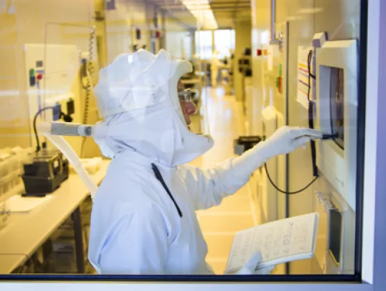
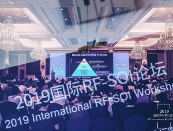
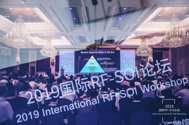
The 2019 International RF-SOI Workshop in Shanghai was packed to overflowing, with over 500 attendees, noted SOI Consortium Chairman Executive Director, Carlos Mazure. There were 16 presentations over the course of the day – every one of them excellent – so it will take two posts to cover them all. We covered Danni Song's compelling keynote in a previous post – see it here. In this post, we’ll cover the remaining keynotes and the morning session, which was dedicated to 5G deployment. In the next post, we’ll cover the afternoon sessions, which were dedicated to the China RF-SOI ecosystem, and the RF value chain. PDFs of the presentations are not yet posted, and then they will only be available to those whose companies belong to the SOI Consortium. But we’ve summarized them all for you, so read on! 
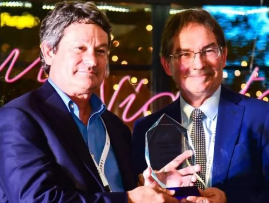
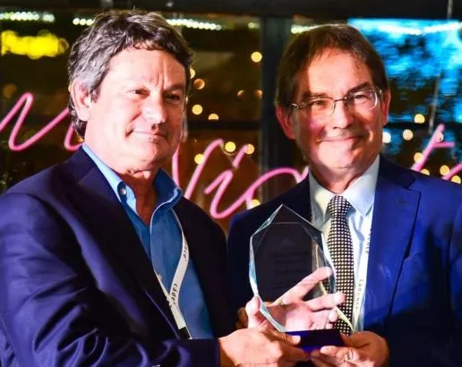
KeynotespSemi: 30 Years of RF-SOI – Past, Present and Future (Jim Cable, Chairman and CTO, pSemi (a Murata company))The keynote by RF-SOI legend Jim Cable chronicled his always-innovating journey from digital to RF via sapphire then SOI. (Cable's work was recognized in an award that evening.) His original vision back in the early days was for a RF front-end module (FEM) + CMOS transceiver. At the time, doing it on sapphire (an insulator) rather than bulk made it much easier, as sapphire eliminated the non-linear capacitances. That was the beginning of their UltraCMOS technology, and though it did very well, sapphire was only available in 6” wafers. So pSemi (or Peregrine, as it was known at the time), engaged with Soitec on bonded-SOS. “It was a killer technology, and the marketshare we won was staggering,” he recalled, and helped convince Soitec RF-SOI was worth looking at. The goal is to handle high RF power levels: you can use SOI to handle higher voltages than you'd think were possible. They added an invention they called HaRP, that dealt with accumulated charges and enabled them to hit the linearity specs on silicon. With that, he explained, they came to completely dominate the switch industry. UltraCMOS evolved, getting 60% smaller with 20x better linearity – but now of course you have 50 switches, not six. He heralded the great partnership they have with GlobalFoundries, noting, “We were pioneers in this field.” In fact, in 2017 they were in the top 10 for IP generation in semiconductor manufacturing. Now comes mmWave, where he says, “We see everything we believed and more.” They're currently sampling an 8-channel mmWave RFFE (RF Front End). Soitec: 5G-on-Insulator: the 5th Gear In Mobile Radio (Michael Reiha, GM, Soitec)Michael Reiha's talk centered on how SOI wafer-leader Soitec is positioning itself on 5G, which, he explained, demands a wider portfolio. Soitec looked at what they could do to make 5G ready for sub-6GHz. Massive MIMO (mMIMO) is an efficient technique to improve throughput. With SOI, you can reduce the power it takes, making it a good choice for urban environments. RF-SOI is a candidate for power amplifiers, and FD-SOI is enabling more users to be added. The concept of network sharing is an opportunity for compact, low-cost filters that can meet the requirements with simpler, lower-cost, higher-efficiency filters. That's why they've just announced a new substrate called piezo-on-insulator (POI). However, total cost-of-ownership is not just how much a product costs, but how much it costs to run it.. Currently, RF and mechanics dominate the bill-of-materials, so you need to decrease the number of RF FEM components and get savings scaled with the array size. The main challenge of SOI is in efficiency, but the advantage is that it can be used in integrating digital with analog sensing and RF. Then you can use AI sensing for tracking temperature, for example, and control for 5G optimization. In short, with RF-SOI, you apply AI to the radio head, especially for things like mMIMO. And btw, he added, Soitec currently has capacity of two million wafers per year. SESSION 1 – 5G DeploymentYole: 5G is ON. Which Impact for RFSOI Technologies? (Cederic Malaquin, Technology Market Analyst)There are over a thousand 5G networks available today worldwide, said Cederic Malaquin. Adoption is accelerating, driven by 5G cloud gaming, AR/VR/XR, 5G multi-video calling and stadiums. However, carriers need better ROI. 5G should address this so that customers are better served. MIMO and carrier aggregation (CA) are the main techniques supporting network capacity and coverage improvements. 5G NR will bring more spectrum. With each generation putting more content in phones, new spectrum is happening in sub6 and mmWave. The impact of 5G on mobile phones is huge in terms of both content and complexity. Some phonemakers (like Apple and Samsung) are moving towards increased integration. Others (like Huawei) are going more for discretes. Yole sees tuners, switches / LNA as addressable by RF-SOI, but they are less convinced about power amplifiers. They also see SiP (system in package) as prevailing over integration. The 5G mobile and base station markets will really build up in 2022-25. RF-SOI will remain the mainstream technology for switches and antenna tuners through at least 2025: they don't see anything else replacing it. There is still increasing demand for 8” wafers. 12” wafers growth comes from integrated switch/LNAs, which comes from the Tier 1's. In the front-end space, Murata leads in dollars by far, followed by Skyworks and others. Though mmWave is not yet clear, there are opportunities for RF-SOI. ST: 5G Deployment Driving RF and SOI Technology Opportunity (Laura Formenti, Sr. Director)STMicroelectronics has a long history in RF-SOI, noted Laura Formenti, dating back to 2000 when they started collaborating with Soitec and Leti. An IDM, ST also offers foundry services. For 5G, their foundry offering includes H9SOIFEM, C65SOIFEM and SOI mmW for high-performance analog, dedicated RF processes for RF switches, LNA, PA plus RFFEM. Then they have FD-SOI for RF, mixed signal and digital integration. From antennas to transceivers there's an opportunity for full integration. For infrastructure, it depends on the customer preferences. 12” C65SOIFEM was introduced in 2019, and 12” SOIMMW will be introduced in 2020. Both their fabs at Crolles and Rousset, France, are in production. H9SOIFEM is for 4G and 5G sub-6GHz RF FEMs, enabling monolithic integration of the PA, LNA and switches, which is especially good for wifi. The C65SOIFEM is high-performance. Panel: 5G Deployment in China, Jeffrey Wang, CEO, Simgui Technology, moderatorWith Danni Song (China Mobile), Jim Cable (pSemi), Peter Rabbeni (GF), YangYang Pen (SmarterMicro), Paul Hurwitz (TJ), Michael Reiha (Soitec)Q: Why sub-6GHz and not mmWave?Danni Song said its a question of available spectrum. In sub-6, you get the same level of coverage with fewer base stations; also, sub-6 is much more mature. When will mmWave be ready? It depends. In the US, yes, but in China the spectrum allocation for mmWave has not yet been done. So it's a wait and see for the industry to be ready. Peter Rabbeni agreed, adding that in the US sub-6 is crowded and conflicts with military bands. Paul Hurwitz added that mmWave is for fixed wireless access. Michael Reiha added that mmWave has advanced a lot even in the last few months (Verizon in Washington, DC, for example), so there is momentum.Q: Does China lead in the sub-6GHz opportunity?Jim Cable said that at pSemi they have two business models: mobile and infrastructure. He sees massive MIMO in base stations as huge (though in mobile their role is more supporting Murata). Peter Rabbeni added that they're working with innovative partners in China, and that GF also offers skills in services and packaging. Yangyang Peng sees big opportunites with 5G for SmarterMicro and China. Paul Hurwitz has seen an increase in the capabilities of RF companies in China, and that the market in China moves faster than elsewhere. Michael Reiha sees China as strategic, and because there is central deployment, they can plan with the right partners.Q: Data usage will be huge – what will it cost to individual users?Danni Song said 5G phones will be expensive, but consumers want them, so we need to bring down costs and increase performance – but what about power consumption? Power needs to come down, maybe levering things like sleep mode more. For 3G 4G, she noted, they had lots of time. People are pushing hard for 5G, but there's a need for patience. Yangyang Peng said he didn't want to pay more than for 4G. In summary, Jim Cable noted that mmWave will demand huge amounts of silicon, to which Paul Hurwitz agreed, and Michael Reiha said Soitec will be ready. Everybody agreed that 3D packaging would be very important, especially for mmWave. And that's it for our coverage of the morning. Next up we'll cover the presentations given during the afternoon.
Read More