downloadGroupGroupnoun_press release_995423_000000 copyGroupnoun_Feed_96767_000000Group 19noun_pictures_1817522_000000Member company iconResource item iconStore item iconGroup 19Group 19noun_Photo_2085192_000000 Copynoun_presentation_2096081_000000Group 19Group Copy 7noun_webinar_692730_000000Path
Skip to main content
Innovations in the public sector are springboards for new products in digital health and personalized medicine. Since 2013, SEMI NBMC, funded by the Air Force Research Laboratory (AFRL), has been evaluating industry needs and soliciting proposals for new research into the foundations of device development and manufacturing of medically actionable devices.SEMI NBMC has run 17 separate programs with more than two dozen organizational participants developing materials, electronics, microfluidics, manufacturing processes and algorithms to create low-cost, wearable sensors. Most of these integrated sensing systems communicate wirelessly and incorporate high-performance silicon devices that are designed to move with the individual. Each of the projects was the result of a proposal received during NBMC’s annual proposal cycle. ​What’s Next in MedTech Device Development?We invite you to join the teams at SEMI, NBMC and AFRL to answer that question in a virtual series of sessions over the four weeks in August.For the past five years, NBMC has been conducting similar sessions for roadmapping the development of non-invasive human performance monitoring technology and manufacturing. The information feeds into the topics for upcoming RFPs, including the one we expect to release in September 2020. Previous Workshops (formerly entitled Blood Sweat and Tears) brought together industry and university innovators to explore current product research and provided excellent insights for the proposal evaluation teams. We believe the insights are also very useful to the business and technology planning direction for researchers and developers working on these products.Our focus is on early-adopting markets – medical professionals and their patients, Army and Air Force personnel and high-performance athletes.​ In this time of social-distancing and overall hesitancy to approach hospitals and medical offices, medical monitoring that provides medically-actionable intelligence is of even greater significance.But Doesn’t FitBitTM Have that Covered?Advancements are coming fast and furious – but medical professionals and insurance companies are struggling to distinguish innovations that provide actionable intelligence from those that provide generalized, non-actionable data.The workshop will focus on the medically relevant information that requires a great deal more accuracy, testing and certification before decisions are made. It is the innovations in this field that will lay the groundwork for new products in digital health and personalized medicine. Additionally, they are leading to advancements in aeromedical monitoring and diagnostics to support the U.S. Air Force’s mission to improve patient care during emergency air transport. The targeted future state is real-time monitoring of biochemical and physiological markers that can guide optimization of human performance and health. ​The SMART MedTech Virtual Workshop Series will link markets with manufacturing for medical relevancy – addressing both ends of the ecosystem. This forum will bring together the players across the growing range of industries that are entering or advancing human monitoring applications to:​ share competitive ideas that may be applied to product development​, assess roadblocks in bringing human monitoring products to market, and form partnerships that have become key in overcoming obstacles to successful manufacturing and product development. ​ Join the experts who are at the cutting edge of product design and manufacturing techniques. Indeed, the success of previous workshops was based on the unique membership of NBMC, where product and manufacturing-oriented engineers from industry, universities, and government labs form teams and pool resources (financial as well as technical) to accelerate human monitoring product development into manufacturing prototypes.Can’t Attend the Workshop?All sessions will be recorded and available for watching and re-watching on-demand. Join our interest list to receive regular updates on SEMI NBMC activities, including notification of the RFP expected to be available in October 2020.Find out more about the Smart MedTech Initiative and the NBMC Programs at our website.Rene Krantz is Director of R D Programs Business Development at SEMI. She is the primary manager of SEMI Smart MedTech Initiative and NBMC programs. Contact Rene at [email protected].
Read More
The COVID-19 pandemic has inflicted major impacts on manufacturing operations worldwide including in the semiconductor industry. The virus has left millions of people confined to their homes, resulting in a massive shift to virtual work and online engagement. In Singapore, where AEM is headquartered, our management team took proactive measures to protect our workers by implementing best practices ahead of the Singapore Circuit Breakers.AEM is globally deemed an essential service, requiring us to maintain operations and minimize impact to our customers. Business continuity plans that include work-from-home and safe-distancing guidelines are in place. As of the time of this writing, we are very fortunate that all of our employees are safe and that we’ve seen only minimal impacts to our customer commitments. AEM has confined this impact by spreading operational risks across our facilities in Asia, Europe, the U.S. and divisions in Singapore, Malaysia, China, North America, Central America, Finland, France and Vietnam. All told, these facilities employ more than 550 people (Figure 1).Figure 1 – AEM Global Presence As a global leader, AEM offers application-specific intelligent system-level test and handling solutions for semiconductor and electronics companies that serve the advanced computing, 5G communications and artificial intelligence (AI) markets.Leveraging our decade of experience, the latest AMPS solutions provide asynchronous, modular, massively parallel and smart system-level testing to meet the new test challenges of complex ICs. The modularity and scalability of these systems enables customers to scale their existing engineering device validation solutions into high-volume, massively parallel production solutions that increase faults coverage, reduces time to market, and decreases cost of test and ownership (Figure 2).Figure 2 – AMPS System-Level Test Solution In meeting 5G infrastructure test needs, AEM developed a field-deployable fiber optics tester. Called WideOptix SR4, the system was initially developed in collaboration with a world leader to support the 5G fiber infrastructure deployment in China and has now been adopted for some Ethernet standards testing. With our WideOptix SR4 development, we cultivated Silicon Photonics (SiPh) testing expertise that complements our AMPS system-level test capability. As part of our business continuation and risk diversifications plan, we had also set up factories in Penang (5,200m2) and Suzhou (3,600m2). Penang’s rising influence in the Southeast Asia semiconductor industry has prompted AMM (AEM Malaysia) to expand its scope to include value-added services with a Center of SSD Excellence and Center of Photonic Excellence.ASZ (AEM Suzhou) will continue to focus on the domestic market in China for further expansion and penetration with products ranging from cost-sensitive testers to state-of-the-art test measurement instruments. In Europe, AEM is focused on wafer-level test and cost-effective ATE test solutions. Finland-based AFORE specializes in MEMS and application-specific wafer testing with the ability to add physical stimulus. The company's state-of-the-art instruments enable the testing of devices such as diced IMU’s (Inertia and Motion Units) in continuous rotation on a wafer mounting ring. Our process increased test throughput by 3X compared to the traditional pick-and-place methods (Figure 3).Figure 3 – Wafer-Level Test Throughput Advantage A specialist in application-specific wafer handling, AFORE developed its latest design to support quantum computing in collaboration with its partner BLUE FORS. The company’s probing equipment features a handling solution with temperature tolerances to 2K (-270’C) to support cryogenic testing (Figure 4).Figure 4 – Cryogenic Quantum Computing Probing Solution AFORE also gained critical insights into creating total darkness, enabling us to further explore opportunities for dark matter testing. AFORE is currently in talks with a member of the LUX Photonics Consortium funded by the National Research Foundation (Singapore) to provide a dark body testing environment and handling for its IR detectors.In Europe, our acquisition of Mu-TEST in France helps diversify our product and service offerings while spreading our business continuity risks. Mu-TEST enjoys collective test-development experience of more than 320 man-years thanks to various ATE suppliers including Schlumberger and Credence. To help combat rising costs of traditional ATE, Mu-TEST developed cost-effective solutions using FPGA-based instruments supported by a full suite of test development, debug and production test software with links to EDA and standard interfaces. This provides Mu-TEST an agile platform that can be easily re-configured for different customer needs.This Mu-Test acquisition expands AEM’s system-level testing capability to include Functional Test, allowing BIST, SCAN, JTAG to test structural failures and perform other application-level test that interface directly with the DUT using the EVM (Electronics Validation) boards to increase fault coverage within the same test environment. Mu-TEST has also enabled AEM to form the recent partnership with UTAC to develop a cost-effective CIS test solution that addresses UTAC’s test needs and complements its CIS advanced packaging solutions. Our U.S. headquarters based in Chandler, Arizona has expanded its capabilities to provide application engineering.In summary, AEM has been expanding its global footprint while managing risk and has been fortunate to be positioned to manage the recent COVID-19 excursions. While each geographical location specializes in core technologies, all sites have access to one another’s manufacturing facilities in times of need and a pool of IP available to address new opportunities. We believe this risk diversification positions us well to serve the needs and interests of our customers worldwide.Lo Wee Tick is Director, Business Development, and Stuart Pearce is Senior Director, Field Marketing, at AEM Holdings Ltd.
Read More
Data recently collected by SEMI points to only a moderate slowdown in the industry’s pursuit of talent, illustrating the growing and significant need for attracting workers at all levels of the organization. With COVID-19’s devastating impact on many sectors of the economy, the time is ripe to sharpen the industry’s focus on attracting and training a new wave of workers to meet the growing talent needs across our industry.To help illuminate the state of microelectronics industry hiring during the pandemic, following are three takeaways from recent workforce development data. Key Takeaway 1 – Emsi Hiring Data and Analytics ReviewIn a May 5 SEMI webinar on the Future of Work, presenter Andrew Crapuchettes, CEO at Emsi, a labor data analytics firm based in Moscow, Idaho, revealed that the U.S. semiconductor equipment and device manufacturing sectors posted 199,326 total jobs (32,022 unique positions) from March through June 2020 with an advertised median annual salary of $68,500 – the highest posting intensity for all other occupations and companies in the U.S. Crapuchettes noted that “although the job postings number was actually down from the previous quarter, some of the large companies have shown flat or growing postings during this period. At Emsi, we are evangelists for more accurately establishing the requirements for the job to more closely match the skills actually being sought.”He pointed to a gap between the skills employers list in job postings and those employees itemize in their resumes. Today’s use of algorithmic resume analysis, however, may reveal false gaps in hiring. Emsi is working with several Fortune 500 companies in the electronics sector to help them analyze their job postings. The goal: to better understand if they have identified the right skills for their business and the recipe for attracting top talent. Emsi supports programs such as the SEMI Works workforce development initiative that are out to more closely align job seekers and curriculum development with the skills needed for microelectronics design, development and manufacturing.During COVID-19, Crapuchettes sees companies across all industries doubling down on employee training. For many organizations, a business slowdown is an opportunity to identify and work to fill employee skill gaps and prepare companies to emerge stronger once the pandemic has passed. Key Takeaway 2 – SEMI COVID Impact SurveyIn March, April and June, SEMI surveyed members to evaluate the impact of COVID-19 and help inform SEMI’s response. Among the questions in the June survey was “How has COVID-19 impacted your hiring plans?” Of the more than 300 respondents, just 13% reported a hiring freeze and 55% said their hiring plans remain unchanged.Figure 2: Data from SEMI COVID-19 Impact Survey All SEMI regions show a similar pattern. Japan, Korea and China reported little to no slowdown in hiring as shown in Figure 2. Differences across regions were notable with more cautious approaches to hiring adopted by North America, Europe and Taiwan, with some companies slowing hiring for certain positions.Key Takeaway 3 – SEMI Survey of Workforce Development Advisory CouncilSEMI relies on members for industry insights we use to build, evolve and prioritize our programs. A June survey of SEMI America’s Workforce Development and Diversity Inclusion Advisory Council showed that, while some member companies have delayed hiring until the pandemic’s impact of the industry is clearer, most respondents see this period as an opportunity to attract talent to the electronics industry and maintain hiring programs to meet the growing demand for talent the digital revolution is fueling. The survey data, as shown in Figure 3, is consistent with Emsi’s results and a larger SEMI member survey. Our June survey also illustrated the strong desire by the Council for SEMI to support diverse communities and lead efforts to connect talent from these groups with career opportunities in electronics. All survey respondents urged SEMI to place the highest priority on promoting Diversity Inclusion in the workforce, with 57% ranking university outreach as a high priority. Visit the Workforce Development Pavilion at Virtual SEMICON West 2020 for More InformationThe microelectronics industry is making a huge impact in the COVID-19 era – from developing the tools to run algorithms for companies working on a vaccine, to keeping the internet humming for home workers and online ordering for homebound seniors. But these services will only continue to evolve at a rapid clip with the right talent. SEMI programs remain laser-focused on pursuing and developing that talent.Thank you to all members who responded to the surveys and Emsi for contributing to understanding of the workforce need in the current climate. We invite all members to connect with SEMI Workforce Development activities. We need your help to align skills to curriculum (SEMI Certs), presenting at our workforce development events and donating to the SEMI Foundation, which provides financial support for much of our work.Learn more about how you can help the industry grow its talent pipeline at the SMART WorkForce Pavilion at the virtual SEMICON West – July 21-23! Checking out the pavilion is free, but there’s a modest fee for the content. Register now for a discounted all-in pass to enjoy blister- and COVID-free access to the first virtual SEMICON West ever. Shari Liss is Executive Director of the SEMI Foundation. She oversees the development and success of all programs from K-12 through re-skilling for veterans.
Read More
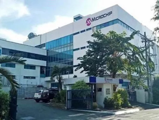
As the COVID-19 quarantine-related restrictions for commerce and transportation are lifted in the Philippines, companies are dusting off desks, cleaning coffee mugs, warming up equipment and gradually bringing back staff to resume full operations. Of primary interest to manufacturing companies like Microchip Technology Philippines are the restrictions on the allowable workforce, the movement of personnel, transportation, and health and safety protocols affecting factory staffing, materials availability, and the ability to ship products. In the Philippines, these restrictions started to scale back in mid-May and are staged to continue in a series of continuing reductions every two weeks through the end of June. As business operations recover, challenges remain in managing the workforce, negotiating the supply chain and understanding the expenses required to operate under the “new norm” while Business Continuity Plans continue to be reviewed and revised.Here are some of the more important business-related elements of the quarantine levels enacted by the Philippines:Enhanced Community Quarantine (ECQ): In effect from March 17 through May 15, 2020, this was the initial lockdown with the strictest requirements, most notably requiring the general population to stay at home, imposing curfews, prohibiting all public gatherings including schools, halting public transportation and banning air travel while allowing cargo flights, skeletal workforces (~15%) for essential businesses (BPOs, IT and exporters, for example) and travel using some private vehicles with varying types of passes required to clear checkpoints.Modified Enhanced Community Quarantine (MECQ): In effect from May 16 through May 31, 2020, this was the first stage to ease control to allow up to 50% of employees to return to work at essential businesses. The easing also allowed gatherings of up to five people while maintaining most other restrictions.General Community Quarantine (GCQ): In effect from June 1 through June 15, 2020, essential businesses are allowed to resume full operations within health and safety protocols in place for physical distancing, disinfection and the wearing of Personal Protection equipment (PPE). Air travel is allowed to resume while public transportation remains restricted until June 21, 2020. Company shuttles are allowed for point-to-point services.Modified General Community Quarantine (MGCQ): Planned for June 16 through June 30, 2020, this is the transition phase to the “new normal,” which will continue easing the restrictions for contact-related businesses such as barbershops, salons, restaurants and the like. Movement and public transportation will remain restricted until June 22, at which point the last obstacle for businesses to fully resume operations will fall.While some larger companies during the most restrictive ECQ were able to house staff on site or nearby in skeletal crews, some smaller companies were unable to do so and may never recover from the loss in revenue or from the loss of employees. The majority of companies in the technoparks shut down under the ECQ and were rendered powerless to return workers to factories. For factories allowed to house employees on site, a huge effort was required to provide emergency transportation, accommodations, food and drinking water, toiletries, Wi-Fi, and even entertainment for the sequestered staff – all while maintaining health and safety protocols for physical distancing and disinfection. For example, Microchip Technology Philippines was able to build temporary sleeping cubicles and showers; to buy tents, foam mattresses, bedding and personal hygiene kits; to provide canteen and laundry services; and to allow Wi-Fi access for employees to stay connected to family and friends.Microchip Technology’s 11 Guiding Values help to define our corporate culture and guide our decision-making. One key Guiding Value on display as we’ve transitioned through the levels of quarantine due to the COVID-19 pandemic has been that Employees Are Our Greatest Strength. Exercising this Guiding Value has supported the expenses necessary to provide the safest, most comfortable living accommodations in the factory conference rooms, hallways, basement, and even in office cubicles.While many larger companies in the Philippines provide company shuttles at pre-established pick-up points, limited public transportation strands many workers at home with no way to reach to their assigned shuttle. To address this challenge, solutions including van brigades that can navigate narrow village streets to pick up workers should be considered though at an additional, unplanned expense. The physical distancing rules effectively halves the number of riders, which in turn requires a doubling of the shuttle buses, most of which are under lease. If shuttle bus leasing companies cannot provide more buses, employees who can work from home should continue to do so or drive to shuttle stops if they have personal vehicles. Leasing these additional shuttle buses was in no company’s budget as we began 2020.Additional measures under the new norm will be expensive – perhaps prohibitively so – for smaller companies that cannot afford to double the number of company transports due to physical spacing rules requiring them to halve workplace capacity, whose workplace environments cannot support physical distancing, and whose treasuries cannot afford to buy rapid test kits for employees and their families. If these smaller companies produce items critical to the supply chain, larger companies will feel the sting – and cease producing specific products during the qualification of an alternate supplier. Until the Bureau of Customs and staffing of third-party logistic providers is back to normal, and until ports are running at full force, materials and exports will continue to be delayed, potentially limiting the number of employees needed to return to work to run production.It has been very expensive for companies to survive through these levels of quarantine while keeping factories and employees in a state of readiness to return to work. Additional expenses will be borne for compliance to the new norm. As many businesses recover under the new norm, they’ll undoubtedly take a closer look at their business continuity planning, if any such plans exist, and if not, they should be created without hesitation.The problem with a typical business continuity plan is it tends to focus on one or a few concurrent major events – say, flooding or a power failure due to a typhoon – but it’s doubtful any plan took into account a global pandemic that affected so many factors simultaneously including workforces, supply chains, transportation, logistics and food supplies. As we return to work, we’ll have to adjust to the new workplace and embed the lessons learned during the COVID-19 pandemic into our business continuity plans. And, hopefully, we’ll never have to exercise those measures again.Greg Fisher is Managing Director at Microchip Technology Philippines.
Read More
Emerging applications powered by 5G and artificial intelligence (AI) are expected to be a boon to the semiconductor industry, but only once chipmakers overcome a key challenge: Architecting chips that meet the exacting performance, power consumption, size and cost requirements of devices for mid- to high-end applications. One technology – heterogeneous integration – promises to meet these demands and help drive future leaps in semiconductor innovation in the post-Moore era. To help the industry better grasp the technology challenges and business opportunities associated with deploying highly integrated chip and packaging technologies, SEMI and AI on Chip Taiwan Alliance recently gathered industry leaders from organizations including ASE, Unimicron, Dialog Semiconductor, Cadence and AITA to discuss technology trends and the vital importance of building a cross-industry exchange platform to advance next-generation manufacturing processes critical to heterogeneous integration. Following are key takeaways from the forum, Heterogeneous Integration Enables 5G and AI. Overcoming Heterogeneous Integration Technology Challenges Key to Advances in Taiwan High-End Semiconductor Manufacturing The introduction of the Heterogeneous Integration Roadmap (HIR) by the International Technology Roadmap for Semiconductors team in 2016 was an important first step, Dr. C.P. Hung, Vice President of ASE Group, noted in his opening remarks. The HIR is designed to stimulate pre-competitive collaboration to advance heterogeneous integration technology development and accelerate electronics innovation. The roadmap provides a long-term vision for the electronics industry, identifying future technology requirements and potential solutions. Today, the HIR working group focuses on high-performance computing (HPC), 5G and other leading-edge technologies.Dr. Hung predicted that heterogenous integration will reshape traditional collaborations between the semiconductor ecosystem and supply chain in order to clear I/O bottlenecks that hamstring high-performance applications. The retooled industry connections will also need to enable high I/O pin counts, ultra-thin devices, and high-frequency signal shields. In an important step forward, the chip industry today is developing a platform that enhances wafer-level advanced packaging services and deepens cooperation with Oversea Assembly and Testing (OSAT) and substrate supply chain partners. Overcoming the current limits of IC substrates – the connection between IC chips the PCB – is one key for heterogeneous integration technology to flourish, said Dr. Yu-Hua Chen, Vice President, Carrier SBU, RD Division of Unimicron. He noted that the industry must tackle limits to PCB thickness, substrate density, fine pitch and automation to meet the needs of high-end packaging customers. Another barrier the industry must be surmounted is to make the currently inscrutable confidentiality requirements for patents of foreign materials – key to improving chip yields – easier to access and understand for substrate engineers. Chen said partnerships across the entire industry will be necessary to break through this and other technology breakthroughs. Supply Chain and Cross-Border Ecosystem to Strengthen Partnerships for Further DevelopmentTaiwan has long invested heavily in advancing semiconductor manufacturing and application engineering technologies to become a top global chipmaking hub and, in the process, has been behind significant leaps in optimizing chip functionality, said Leroy Liu, General Manager, Asia Headquarters, of Dialog Semiconductor (Germany). With its semiconductor manufacturing prowess, Taiwan can also play a central role in maturing advanced heterogeneous integration packaging technology while managing development costs by partnering with its international supply chain community to overcome technical challenges more effectively, Liu said. The region can also help forge partnerships, even among competitors, to build the ecosystem essential for heterogeneous integration technology to shine.EDA tools will be critical in understanding and resolving heterogeneous integration technical issues since IC substrate, packaging and chip design all pose interdisciplinary engineering challenges, said Julian Sun, Product Marketing Director at Cadence. To help the industry navigate these challenges, Cadence has launched intelligent system design products – solutions that address a wide range of design problems with semiconductor nanometers, micrometers on packaging and testing, and PCB level micro/millimeters to Pin/Pitch, I/O models, and thermals and electricity. By supporting various technical designs, Cadence helps customers shorten the design cycle to strengthen design quality and reduce costs.Sun also pointed to the vital importance of overcoming the significant challenge of designing silicon interposers for heterogeneous integration. Today’s EDA tools are capable of optimizing the design of complex structures including 5GAiP and HBM and are instrumental in aiding Taiwan’s semiconductor ecosystem players to quickly adapt to shifts in the evolving heterogeneous integration market.Heterogeneous Integration Enables 5G and AI speakers (L-R): Julian Sun, Product Marketing Director at Cadence, Dr. Yu-Hua Chen, Vice President, Carrier SBU, RD Division of Unimicron, Dr. C.P. Hung, Vice President of ASE Group, Leroy Liu, General Manager, Asia Headquarters, of Dialog Semiconductor (Germany), Dr. Shih-Chieh Chang, AITA Executive Secretary Designing AI chips is particularly difficult as semiconductor makers struggle with high costs and low yields, said Dr. Shih-Chieh Chang, AITA’s Executive Secretary. That’s why the chip industry now uses FPGAs for small-volume production of AI chips, which makes it easier to improve manufacturing yield through redundant design. For its part, AITA has formed a special interest group (SIG) to help form connections among the chip industry, academia and research institutes. The association’s goal is to build a platform for mass production of AI chips.To get involved in SEMI Taiwan Heterogeneous Integration related events, please contact Ula Huang, outreach senior specialist, at [email protected] Fang is a coordinator and Ashley Huang is a specialist in marketing and public relations at SEMI Taiwan.
Read More
Many companies are applying Fourth Industrial Revolution initiatives in manufacturing, though only a few have managed to successfully integrate the smart manufacturing technologies at a scale that allows them to realise significant economic and financial benefits.Known as lighthouse companies, these organisations have taken their smart manufacturing journeys from pilot to integration at scale, serving as beacons to others in overcoming challenges in their production systems through the adoption of leading-edge technologies such as artificial intelligence, additive manufacturing and advanced analytics.At the recent SEMI Southeast Asia webinar Journey to Recovery of the E E Industry, Dato' Azman Mahmud, Chief Executive Officer of Malaysian Investment Development Authority (MIDA), spoke about building Malaysia’s very own Lighthouse Project comprising multinational corporations that will act as anchors to help guide local players into this new venture.During the webinar, Dato' Azman elaborated about Malaysia’s competitive edge – its diversified economic structure and government support. He said the key to sustaining this competitive edge, however, is that the Malaysian economy must be digitally empowered. The Lighthouse Project is one programme that will help achieve this objective. We are inspired and encouraged by this initiative. As firm believers in connecting and collaborating, SEMI Southeast Asia supports programmes that advance the entire microelectronics ecosystem. We look forward to seeing MIDA drive this project, and we encourage Malaysian E E companies to tap MIDA’s expertise in this field. Ultimately, we are confident that through this initiative and the adoption of Industry 4.0 technologies, Malaysia will be repositioned as a top global manufacturing nation. Bee Bee Ng is president of SEMI Southeast Asia.
Read More
By Sowmyan Rajagopalan, Founder and CTO, Thalia Design Automation FD-SOI is receiving significant traction with analog designers, but analog IP reuse often equates to tough choices. Porting chips from bulk to FD-SOI or creating new chips on FD-SOI means making decisions on porting existing bulk IP or starting from scratch. To invest the time and resources in reusing an analog IP requires a judgement call on the potential returns from the market and the time it takes to get the IP to that market to generate revenue is key – if a competitor's project hits the market first, then the potential returns are greatly diminished. There is also a need to understand the differences in process technologies and the impact those differences have on the efficient reuse of analog IPs. All this means that the demands on resources and time are high. Decisions, decisions A typical decision fork faced by many companies is whether to design new IPs, or if they should instead build a portfolio of analog IPs. Given the opportunity cost, availability of resources, time and resources needed for each option means that doing both is a difficult option. Both have their advantages; designing new IPs allows companies to branch out and address new sectors or markets. New IPs often demand higher revenues and engages in-house designers as the work, by its nature, is more innovative and challenging. On the other hand, building a portfolio of analog IPs allows companies to expand in an existing market, bringing stabilisation and strengthening revenues from existing product sectors. But why should you have to choose when there’s a third option? Have your cake and eat it It is difficult for a company to drive both options internally – not least because there’s a paucity of good analog designers in the market, and the opportunity cost is simply too high. However, the good news is that firms like Thalia have the specialist expertise and toolsets required build a portfolio of analog IP, saving time and investment while in-house designers focus on new IP design. Looking back Over the last 18 months, there has been a rapid uptake of FD-SOI process technologies. With production at foundries such as GlobalFoundries and Samsung now in full swing, more and more analog designers are reaping the benefits of FD-SOI. At Thalia we’ve been at the forefront of some of these changes, having worked with multiple customers on projects that use FD-SOI technology. [bctt tweet="More more analog designers are reaping the benefits of #FDSOI. At Thalia we’ve been at the forefront of some of these changes, having worked with multiple customers on projects that use FD-SOI technology. - @Thalia_IP_Reuse CTO " username="soiconsortium"] Driving the shift to FD-SOI [caption id="attachment_34410" align="alignright" width="347"] (Courtesy: STMicroelectronics)[/caption] This figure contrasts the structures of traditional bulk planar and SOI type transistors. The main difference is the inclusion of a buried oxide layer that isolates the channel of the transistor from the bulk silicon of the substrate. This results in a very thin, controllable channel structure, with much lower leakage currents being ‘lost’ into the device substrate than traditional alternatives. This in turn improves two key figures of merit for the device. First, standby power consumption is dramatically reduced. Second, the threshold voltage is much more predictable and controllable – yields are improved, and power/performance tradeoffs via voltage scaling are more easily enabled. The penalty is that FD-SOI transistors are generally not so fast. But one other feature of the technology – particularly important for mixed signal and analog designs – allows smart designers to mitigate this effect. Biasing the body structure at a different voltage to the source enables the designer to trade speed for power: a reverse bias increases the threshold voltage of the device, making it slower, but reducing leakage current; conversely, forward biasing reduces the threshold voltage, increasing the speed of the device, at the cost of power. Design migration Thalia has worked on a number of projects that utilize SOI technologies. A recent RF front end for Bluetooth Low Energy (BLE), for example, used exactly the techniques I have outlined above. We migrated an entire subsystem design, composed of around 30 blocks (including ADCs, PLLs, mixers, amplifiers and power controllers), to a 28nm Samsung FD-SOI process. [caption id="attachment_34412" align="alignright" width="451"] Click on this slide to see a YouTube video of the full Thalia presentation given at the Design Reuse FDSOI Virtual Event in March 2020.[/caption] The circuit was verified for compliance with design specifications. Design changes were implemented to ‘nudge’ the design to meet the requirements. And we made full use of the body biasing techniques I have already outlined. We used reverse body biasing to keep leakage as low as possible in parts of the circuit in which speed was not a factor; and, where speed was a key requirement, implemented forward gate biasing to increase performance. We’re expecting increasing numbers of customers to start moving their analog and mixed signal designs to SOI technologies in the coming months and years. The process is not without its challenges: but with an intimate knowledge of circuit design and optimization, and of the subtleties of the processes themselves, there are substantial advantages to be reaped. Technology analyzer – identifying the root cause when circuits fail A large part of the effort involved with migrating an IP from one technology to another is involved with qualifying the IP in the target technology; if a block doesn’t meet the requirements of the target technology, it won’t function. Identifying the cause of this – the technology characteristics that cause it – and then addressing them is key to a successful outcome. Whenever a key specification is not being met in the target technology, we have to determine which process technology or circuit characteristic is causing this. By using our automated technology analyser, we can take a design-centric approach to analyse and compare base and target technologies to see where the process technologies are similar and where they differ the most. The technology analyser considers both first and second order effects including FT, gm/id, Vdsats among others. Using this technology, we can identify which characteristics differ between the origin and target technologies. With traditional methods, identifying differences in characteristics would be time consuming, but our technology analyzer gives a clear and rapid identification of the issues, allowing us to fix any mis-matched topologies and achieve a functioning result in the target technology. The reality? IP reuse is not a dream or a myth Our platform comprises three elements – Technology, Methodology and Design Expertise. Using this trifecta, we have been able to deliver IPs in different technologies, nodes and with improved characteristics. The AMALIA technology consists of four elements: a technology analyzer, schematic porting, design enabler and layout migration. Tech analyzer: Using a design-centric approach, the platform addresses key first and second order effects of process technologies and extracts and compares characteristics between base and target technologies to provide the user with clear inputs on how similar the technologies are. Automated schematic porting: Taking the inputs from the analyzer and generates a circuit in the target technology. This circuit can then be verified for response and characteristics. Design enabler: Once the circuit design for the target technology is correct, the design enabler and our team of experienced designers can nudge the circuit back into specification. Layout migration: The final stage is focussed on putting together the base layout framework which is then expanding on by our experienced layout designers. Who we are?We are Thalia Design Automation. I founded Thalia in 2011, with the aim of improving the efficiency and process cost of analog circuit design and to rollout an analog IP reuse platform. We’ve worked with vendors, numerous foundries and different nodes and have design centres in Germany and India with our headquarters in the UK. We have successfully rolled out an analog IP reuse platform that combines smart technology, a smart methodology and our smart and experienced resources to streamline the IP reuse process. In doing all this, Thalia regularly provides customers with a time saving of around 50% compared to a traditional circuit redesign. And as I stated at the beginning of this article, achieving a faster time to market is key to maximizing revenues from any IP.
Read More