July 21, 2026 - July 23, 2026
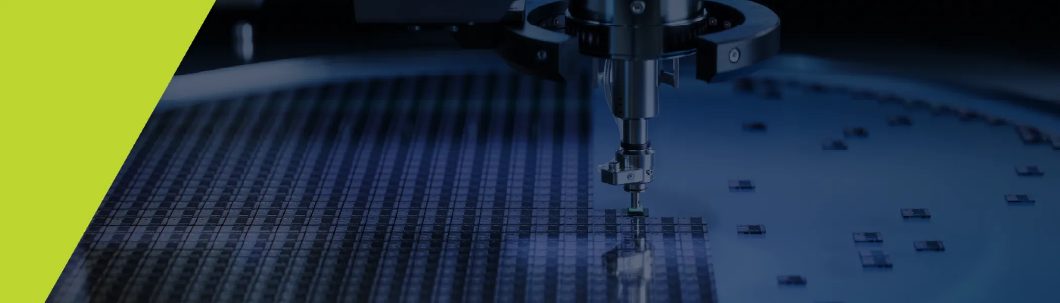
Unlock the essentials of the semiconductor manufacturing process. We will cover science and engineering concepts needed to understand device manufacturing.
Pricing
Early Bird Pricing: $100 off
- Members:
$699$599 - Non-Members:
$749$649
* For group orders with 10+ attendees, and for Students/Veterans discounted pricing, please contact [email protected].
Time
8:00 am - 12:00 pm PDT
Location
United States
Course Description
This three-day virtual workshop (4 hours a day) provides a complete overview of the semiconductor manufacturing process. The class focuses on key process steps needed to form a functioning device. Some important science and engineering ideas needed to understand device manufacturing will be discussed. The workshop is designed for non-technical personnel needing an understanding of the fab process steps. Some technical background from attendees will improve the workshop learning.
The first day will overview the fab process steps with a brief summary of how a transistor functions. We will discuss how multiple transistors are connected to form a logic or memory device. We will also cover how a transistor works with respect to the physical layout of Bipolar and MOSFET transistors.
The second day will cover key fab process steps. Ion implantation, photolithography including DUV and EUV processes, plasma processes including deposition and etch, rapid thermal processing, and wet etch processing. Specific emphasis will be given to the different wet etch processes.
The third day of the workshop will focus on the new transistor designs, including FinFET and CFET designs. We will also cover reasons for changing the transistor design and newer materials, including tantalum, hafnium, silicon germanium, and low-k dielectrics. We will also review roadmaps of leading companies, including TSMC, Intel, and Samsung.
After completing the workshop, the student will be able to describe all the fabrication and assembly process steps and have an understanding of how the process steps work together to form the completed integrated circuit, in addition to an understanding of future structures.
Who Should Attend
This course is intended for both manufacturing and R&D know-how in IC packaging professionals, including but not limited to:
- Process Technicians
- Material Engineers
- Process Engineers
- Equipment Manufactures
- Technical Marketing Engineers
Topics Included
- Silicon wafer manufacturing
- Basic operating principles of transistors and semiconductor devices
- Planar, FinFET, and GAA transistor formation and design differences
- Fab processes needed to form a semiconductor, including the following:
Important Information
Note that only the person who registered will receive a certificate of completion. This virtual training will not be recorded. Attendees must be present to access the course knowledge.
Can't find the training link on the day of? After you register, you will receive the link to the live training via the email address you provided. In addition, you will receive email reminders about 24 hours in advance and an hour before with the same link. Please keep these emails on hand to access the training on time. If you do not see any confirmation emails, please check your junk/spam folders before contacting SEMI U for support.