downloadGroupGroupnoun_press release_995423_000000 copyGroupnoun_Feed_96767_000000Group 19noun_pictures_1817522_000000Member company iconResource item iconStore item iconGroup 19Group 19noun_Photo_2085192_000000 Copynoun_presentation_2096081_000000Group 19Group Copy 7noun_webinar_692730_000000Path
Skip to main content
Default Banner Image

300mm

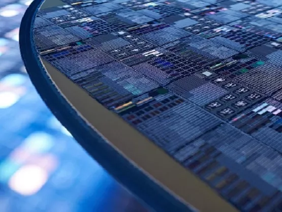
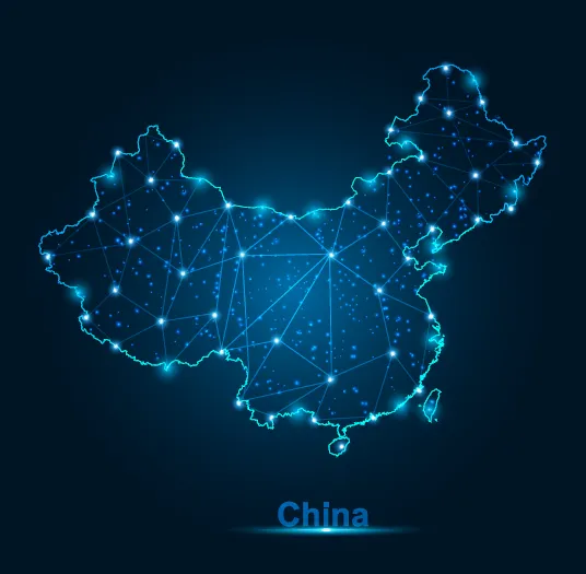
Region’s Fab Capacity Expansion Picks up PaceUnwavering in its drive to build a strong, self-sufficient semiconductor supply chain, China plans more new fab projects than any other region in the world from 2017 to 2020, and its expansion of fab capacity recently picked up pace on the strength of new foundry and memory projects from both domestic and foreign companies, according to SEMI’s 2018 China Semiconductor Silicon Wafer Outlook report. China’s installed fab capacity is forecast to grow at a 12 percent CAGR from 2.3 million wafers per month (wpm) in 2015 to 4 million wpm in 2020, faster than all other regions.Well known for its semiconductor packaging prowess, China in recent years shifted its focus to front-end semiconductor fabs and a few key material markets. In 2018, the region’s surge in fab investment thrust it past Taiwan as the second largest capital equipment market in the world, behind only Korea. However, China’s semiconductor manufacturing growth faces strong headwinds. Chief among them is the tight supply of silicon wafers over the past two years due in large part to the sector oligopoly’s firm control of global production, with the top five wafer manufacturers accounting for over 90 percent of market revenue. In response, China’s central and local governments has made the development of its domestic silicon wafer supply chain a key initiative, funding multiple silicon wafer manufacturing projects.According to the 2018 China Semiconductor Silicon Wafer Outlook report, many of China’s domestic silicon suppliers capably provide wafers 150mm in size and smaller. And the while the region lags peers in 200m and 300mm processing technology and capacity, strong domestic demand and favorable policies have fueled progress in 200mm and 300mm silicon manufacturing with some Chinese suppliers having reached key large-diameter manufacturing milestones.However, it will take these new suppliers several years before they can meet capacity and yield requirements of the larger-diameter silicon wafer market. Company plans and announcements indicate that by the end of 2020, total silicon supply capacity in China will reach 1.3 million wpm for 200mm, possibly leading to a slight oversupply, and 750,000 wpm for 300mm.China’s equipment suppliers, particularly crystal furnace vendors, are also investing in the development of 300mm wafer manufacturing, and domestic tool suppliers have developed most of the necessary tools for wafer manufacturing, except for inspection.While China’s silicon wafer suppliers continue to lag international peers in manufacturing capabilities, the region’s silicon manufacturing ecosystem is maturing and becoming better integrated. The sector’s growth is driven and accelerated by significant domestic market demand and favorable policies.About the China Semiconductor Silicon Wafer OutlookSEMI’s 2018 China Semiconductor Silicon Wafer Outlook is a comprehensive research report with a Microsoft Excel® workbook containing in-depth analysis of China’s silicon wafer manufacturing ecosystem as it relates to the global semiconductor wafer industry. The report covers the latest developments in China’s silicon wafer supply chain, including details on the rise of China’s silicon manufacturing, polysilicon, and silicon wafer-related equipment companies. The report also examines policies, funding and their implications for China’s silicon wafer supply chain.Clark Tseng is director in Industry Research and Statistics at SEMI.
Read More
Device manufacturers continue to invest. Spending in cloud data center (compute, networking and storage), automotive (content per car increases), industrial (on content, factory automation, and positive macro trends), and consumer (gaming) end-markets is particularly strong. We see capital expenditure growth in 2018 and early indications pointing to sustainable spending into 2019. We also expect 14 percent increase (YoY) for fab equipment spending in 2018, up from the February forecast of 9 percent, and expect 9 percent increase in 2019, adjusted from the February forecast of 5 percent. 92 future facilities/lines with various probabilities are scheduled to start production in 2018 or later. Fab investment is just one indicator of how growing demand in areas such as from Artificial Intelligence (AI), cloud/data storage, automotive and Internet of Things (IoT) is driving unprecedented spending in the semiconductor industry. Below are a few highlights* of recent SEMI FabView insights. Details of each project can be found in FabView online 24/7 or World Fab Forecast report (Excel format). Infineon’s new 300mm Fab in Austria - Infineon is planning a new 300mm thin wafer Fab for Power Devices in Villach, Austria. Rumors on Toshiba’s new Fab plans - More 3D NAND fabs in the future at Toshiba are feasible. The timing will depend on market conditions, and our forecast will adjust accordingly. Vanguard's possible 300mm foundry fab - Vanguard's management said it might buy or build a 300mm fab in the near future as all 200mm fabs are essentially full. Powerchip plans to build new memory fab in Taiwan - Powerchip is investing more in expansions since Memory pricing is holding up. Rohm announced to build a new SiC fab in Fukuoka Japan - Rohm announced its plans to build a new SiC fab. Micron is building a new fab in Singapore - Micron broke ground in a ceremony for a new fab in Singapore on April 4, 2018. Bosch had groundbreaking ceremony of their 300mm fab in Dresden end April 2018 - Investment of 1 billion Euro. This is the biggest single investment in Bosch’s 130-year history. SEMI FabView, a mobile-friendly, interactive version of SEMI’s popular World Fab Forecast, delivers on-demand fab information such as fab spending and capacity for over 1,100 facilities, including over 82 planned facilities worldwide, across a wide range of product segments including Power, GPU, Memory, Foundry, MEMS and Sensors fabs. Fab data include region, start of construction, operation, construction and equipment spending, capacity, wafer sizes, product types and geometries. SEMI FabView subscribers receive forecast model updates through SEMI’s World Fab Database. Click here for a trial to experience SEMI FabView first hand. *Actual updates provide more detail Christian G. Dieseldorff and Clark Tseng, Industry Research Statistics Group, SEMI.
Read More