downloadGroupGroupnoun_press release_995423_000000 copyGroupnoun_Feed_96767_000000Group 19noun_pictures_1817522_000000Member company iconResource item iconStore item iconGroup 19Group 19noun_Photo_2085192_000000 Copynoun_presentation_2096081_000000Group 19Group Copy 7noun_webinar_692730_000000Path
Skip to main content
Default Banner Image

TEL

SEMI spoke with Eyal Shekel, senior vice president of Service Strategy and Excellence at Tokyo Electron Limited, about the impact of artificial intelligence (AI) on smart manufacturing and how other fab solutions for smarter process tools are advancing semiconductor manufacturing.Eyal shared his views ahead of his presentation at the SEMI Fab Management Forum, 17 February, as part of the SEMI Technology Unites Global Summit, 15-19 February 2021, an online event. Join us to meet experts from Tokyo Electron and other key industry influencers. Registration is open. SEMI: AI technology is considered a key enabler for smart manufacturing. What are the latest trends? Shekel: The advent of advanced nodes and extreme complex 3D semiconductor geometry has lengthened time to market and increased costs in areas ranging from equipment development and large-scale metrology usage to monitoring yield inhibitors.AI is becoming a critical tool in the area of material informatics to determine suitable materials and processing techniques in order to meet the needs of future devices. Together with new materials and processes, the development and implementation of virtual metrology will enable accurate and almost absolute real-time monitoring of our customers’ device wafers at each stage of the manufacturing process.SEMI: What are the benefits of data analysis in the process from R D and Ramp-Up to High-Volume Manufacturing? Shekel: The new research field of materials informatics enabled by AI provides tools to guide the highly efficient discovery and optimization of production processes. For example, TEL has developed methodologies for co-optimizing processes and materials for etch rates.To monitor and manage the yield of semiconductor fabrication processes, direct metrology measurements are important. However, it is difficult to monitor all production wafers due to the time and cost involved. With deep learning AI, it is now becoming possible to predict every wafer’s metrology measurements based on production equipment data and previously processed wafer metrology variables. This enables total quality management and run-to-run control, while simultaneously reducing production costs and cycle time.SEMI: Can you tell us more about TEL Service Advantage?Shekel: TEL Service Advantage is a TEL global support organization that allows customers to select a service plan that fits their needs. Through TEL Service Advantage, we can quickly respond to customer requests and technical advancements. TEL Service Advantage provides various plans to maximize equipment maintenance efficiency for customers and productivity from equipment manufactured by TEL. TEL Service Advantage plans can be combined to meet customer needs and achieve maximum results.A key enabling element of TEL Service Advantage is TELeMetrics™. TEL analyzes equipment data from various sensors using a remote connection and, based on that analysis, provides solutions to customer-specific problems around equipment throughput and predictive maintenance.SEMI: How is AI helping during the pandemic? Can you share a success story? Shekel: The pandemic forced severe travel restrictions worldwide, making it very difficult or even impossible in many cases to visit our customers, as it is still the case today. Standard communication devices like smartphones and email helped at the beginning when TEL intensified the remote support by our Total Support Centre (TSC).TEL continued to develop its Service Advantage program quickly, and started using additional advanced tools and methodologies such as the following: Deployed AR (Augmented Reality) to remotely assist our customer and TEL engineers Secured remote connections into TEL tools to investigate parameters and logs, or to change set-up Used remote training courses that connects trainers via video conferencing systems and training tools in the factories to skill up engineers located in a different parts of the world Used AR glasses for tool start-up and troubleshooting Expanded TEL database global technology with multi-tool on languages search capabilities A key project at a customer site in Europe offers an excellent success story. Using all the approaches above, we collaborated with the local team to put a tool into production with no major delays. This was highly appreciated by the customer and very important for us.SEMI: What do you predict for the future? Shekel: Global technology infrastructure continues to develop and expand rapidly. Elements like 5G networks, IoT and advanced sensing capabilities will lead to what we call General AI, which will be based on neuro-like infrastructure. The auto learning will spread across domains and rely on internal logic and reasoning to automate many tasks that are manual today. In our industry in particular, General AI will enable workers to focus more on data analytics and future advanced R D rather than ongoing operations.SEMI: How can technology unite us? What do you expect from your participation at SEMI Technology Unites Global Summit?Shekel: Technology united us in the last 150 years. The connectivity started with telegraph and telephone and was used to exchange information over wider distances. Nowadays, video conference capabilities, AR and improving communications technology makes it much easier to unite people who are geographically dispersed. This becomes obvious and valuable especially during this pandemic period. As a fact, we are able to continue to perform all our key activities – our tool support, training and customer relationships – even if we cannot be present in person.The SEMI Technology Unites Global Summit is a great chance to stay connected to people and customers that I would normally meet at the SEMICON exhibitions.It also offers the opportunity to network with many more people who I would not be able to meet otherwise. Moreover, I can watch speeches and presentations at any time! Normally I would miss some programs since exhibitions and events took place at the same time.Eyal Shekel, senior vice president of Service Strategy and Excellence at Tokyo Electron Europe Limited, is a 27-year semiconductor industry veteran. Upon his graduation as a Mechanical Engineer from the Technion (Israel leading technical institute), he joined Applied Materials. In 1997 he moved on to Tokyo Electron (TEL) in Europe, served as the Regional Service Manager of Israel and, soon after, was appointed the company’s General Manager. Since 2005 Eyal has been part of TEL Europe senior management. He oversaw the Service and Support Operations for TEL Europe as a senior vice president until 2019. In his current role, he co-leads TEL’s Global Service Committee in Japan.The SEMI SMART Manufacturing Initiative is a global effort to promote awareness of and interest in smart manufacturing with a focus on delivering industry-recognized best-in-class programs and services to enable members to maximize product quality and productivity while reducing costs. Activities are focused on building out core capabilities to enable smart manufacturing across the microelectronics supply chain. MADEin4 is a consortium of 47 partners from 10 countries connecting the full range of supply chain – from semiconductor equipment manufacturers and system-integrating metrology companies to RTOS and key applications such as the automotive industry. The MADEin4 Project develops next generation metrology tools, machine learning methods and applications in support of Industry 4.0 high-volume manufacturing in the semiconductor manufacturing industry. Serena Brischetto is senior manager of Marketing and Communications at SEMI Europe.
Read More
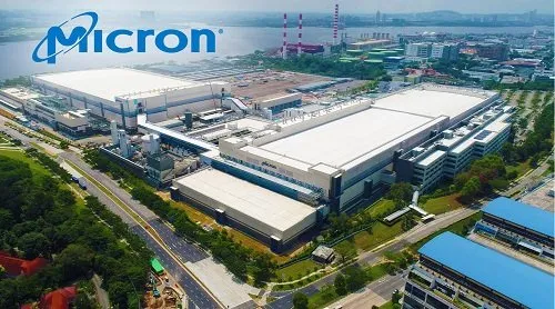
Making Strides TogetherKnowledge is power – especially when it is shared. This principle formed the foundation for Micron’s Go and See virtual visit of its Singapore manufacturing plant on 26 August 2020 as 27 companies including GLOBALFOUNDRIES, ST Microelectronics, Infineon, TEL, ViTrox , IBM, HP and UTAC joined the first-of-a-kind virtual factory visit. The chip industry powerhouses gathered to see how Micron’s Lighthouse frontend wafer fabrication facility leverages Fourth Industrial Revolution technologies to drive new production and cost efficiencies.They saw clear markers of a transformed organisation and spoke with working-level staff, managers and front-line employees. Company representatives also met virtually with Micron management teams from organisations that led its digital transformation – from pilot programs to integration at scale – to realise significant financial and operational benefits. The mix of technologies they deployed to make it all happen included artificial intelligence (AI), big data analytics and the Industrial Internet-of-Things (IIoT).Micron’s Singapore-based fab facility earned Lighthouse certification earlier this year from the World Economic Forum’s Global Lighthouse Network. The Go and See tour was co-sponsored by SEMI Southeast Asia and McKinsey Company.Transformation is CrucialBy embracing Lighthouse principles, semiconductor sectors and companies can accelerate their digital transformation to boost operational and financial efficiency while helping increase productivity across the electronics supply chain. It will take time for Southeast Asia semiconductor manufacturers to transform to digital operations, though we’re seeing growing interest in Industry 4.0 practices as they begin to understand that the deployment of new technologies and applications will help them better understand real-world benefits of smart manufacturing use cases and solutions. SEMI believes shining the spotlight on companies like Micron can illuminate the way forward for other companies to help drive the industry’s digital transformation. We look forward to seeing companies build on this momentum as they start to leverage leading-edge technologies to improve efficiencies and promote sustainability.Bee Bee Ng is president of SEMI Southeast Asia.
Read More
Would you buy your next hotdog in parts, from un-coordinated suppliers? For example: Get the bun from a baker, the sausage from a butcher, mustard and/or ketchup and veggies from the nearest supermarket? If yes, you may find the sausage being too small, the veggies too big for the bun, and, when you finally finished adding mustard/ketchup and start eating, you may “enjoy” a cold sausage on a soggy bun!This “hotdog example” is just a very simple way to highlight the advantages of a well-coordinated semiconductor supply chain. What may be a few dollars and cents wasted in this hotdog purchase, can become millions of dollars lost to delays and inefficiencies during the roll-out of a new electronic system.Complexity is Increasing the ChallengeThe very innovative semiconductor industry is continuing to develop more complete and complex building blocks for electronic system solutions, with the intent of making our customers’ lives easier. However, every new technology takes increasingly more time for technical and business interfaces to mature before all the semiconductor supply chain members can serve customers in a smooth, efficient and cost-effective manner. In particular, coordination between design and manufacturing has always turned out to be in the critical path.SEMI, the manufacturers’ trade organization, and the Electronic System Design (ESD) Alliance, representing electronic design automation (EDA) tools vendors, developers of intellectual property (IP = ready-made building blocks for ICs) and IC design service providers, both recognized these challenges. Late in 2018, these two industry organizations decided to jointly address this painful, costly and often a very frustrating, yet critical path and became Strategic Association Partners, The goal is to establish a well-coordinated semiconductor supply chain.To make the value propositions of this partnership highly visible and demonstrate the first joint accomplishments, SEMI’s well-known SEMICON West conference and, in its first year, ES Design West, will be conveniently co-located in San Francisco’s Moscone Center from July 9 to 11, 2019. The synchronized schedules and geographic proximity of these events not only outlines the multi-faceted interdependence of manufacturing and design but encourages and enables conference attendees to do, what previously would have been viewed as “forming cross-border relationships.” It’s a new word now — please join the path to success and expand your network!Navigating SEMICON West and ES Design WestJust in case you are not yet planning to come to San Francisco early July, please check the Agendas-at-a-Glance for SEMICON West and ES Design West, to see how broad and valuable these parallel conferences are for your business. In addition, every customer, partner and semiconductor industry supplier can, from July 9 –11, walk from one conference section to the other, arrange face-to-face meetings, in dedicated meeting rooms, with representatives from both camps and discuss, from the first project planning step to the final production ramp-up, the many topics that need to be coordinated across parts or the entire supply chain to minimize delays and/or cost over-runs.Who Will Lead the Discussions?Conference attendees can, in addition to meeting many important supply chain partners face-to-face, hear about the latest technologies and market trends from key executives in our industry. Featured speakers are: David Pellerin, Head of Global Business Development, Amazon Web Services Lisa Su, President, and CEO, AMD Gary Dickerson, President, and CEO, Applied Materials Laurent Le Faucheur, Principal Engineer, Digital Signal Processing and Machine Learning, Arm, Ltd. Renee St. Amant, Ph.D., Research Engineer in Emerging Technologies and US Innovator of the Year, ARM Dean Kamen, President DEKA Research Development, Founder First and First Global Jeffrey Welser, Ph.D., Vice President and Lab Director, IBM Research-Almaden Dean Drako, President and CEO, IC Manage, Inc. Oreste Donzella, Sr. VP Chief Marketing Officer, KLA Corporation Prakash Narain, President, and CEO, Real Intent, Inc. Aart de Geus, Chairman, and Co-CEO, Synopsys, Inc. Manish Pandy, Fellow, Synopsys, Inc. Nate Baxter, General Manager, Development and Production Group, TEL US Like in previous years, SEMICON West and ES Design West offer a range of special features, addressing Smart Manufacturing, Smart Transportation, Smart MedTech and Smart Workforce development in dedicated pavilions as well as an AI Design Forum. Also, the many exhibitors from both camps will give conference attendees convenient opportunities to get to know new supply chain partners and/or refresh long-term business relationships. Search for the exhibitors you want to meet early July here. Questions to Ask for a Well-Coordinated Semiconductor Supply ChainIf I may, I would like to ask my many friends in the manufacturing camp to spend some time in the ES Design West section and ask the exhibitors a few questions, like: What can you do to get me to profit faster? To reduce development and unit cost? To improve yield, product quality, and reliability? When can you visit my team to discuss how your company can contribute to our goals?Vice versa, I would like to encourage my friends in the design camp to spend time in the SEMICON West section and ask exhibitors what their companies offer. When talking to manufacturers of IC, passive components or circuit boards, assembly and test houses, please ask very specific questions like: How can we help you reduce iterations between you and your customers? How can we help to improve IC test programs? How can we increase the throughput of your manufacturing equipment? How can we apply machine learning (ML) and Artificial Intelligence (AI) to minimize equipment downtime, improve yields and/or shorten production ramp-up?I can assure you that you’ll not only win great friends “across the border” but will be very impressed by the expertise you’ll find in the other camp and the willingness for and benefits of cross-border cooperation.I look forward to meeting you at SEMICON West and ES Design West. Also, if your schedule allows, mark your calendars for the June 12 MEPTEC Luncheon at SEMI in Milpitas, June 18 for the GSA’s Silicon Summit in Santa Clara and June 25 to 27 for the IMAPS SiP Conference in Monterey, CA. Hope to see you at one or all of these important events!Article originally published in 3D InCites. Herb Reiter is president of eda 2 asic Consulting.
Read More
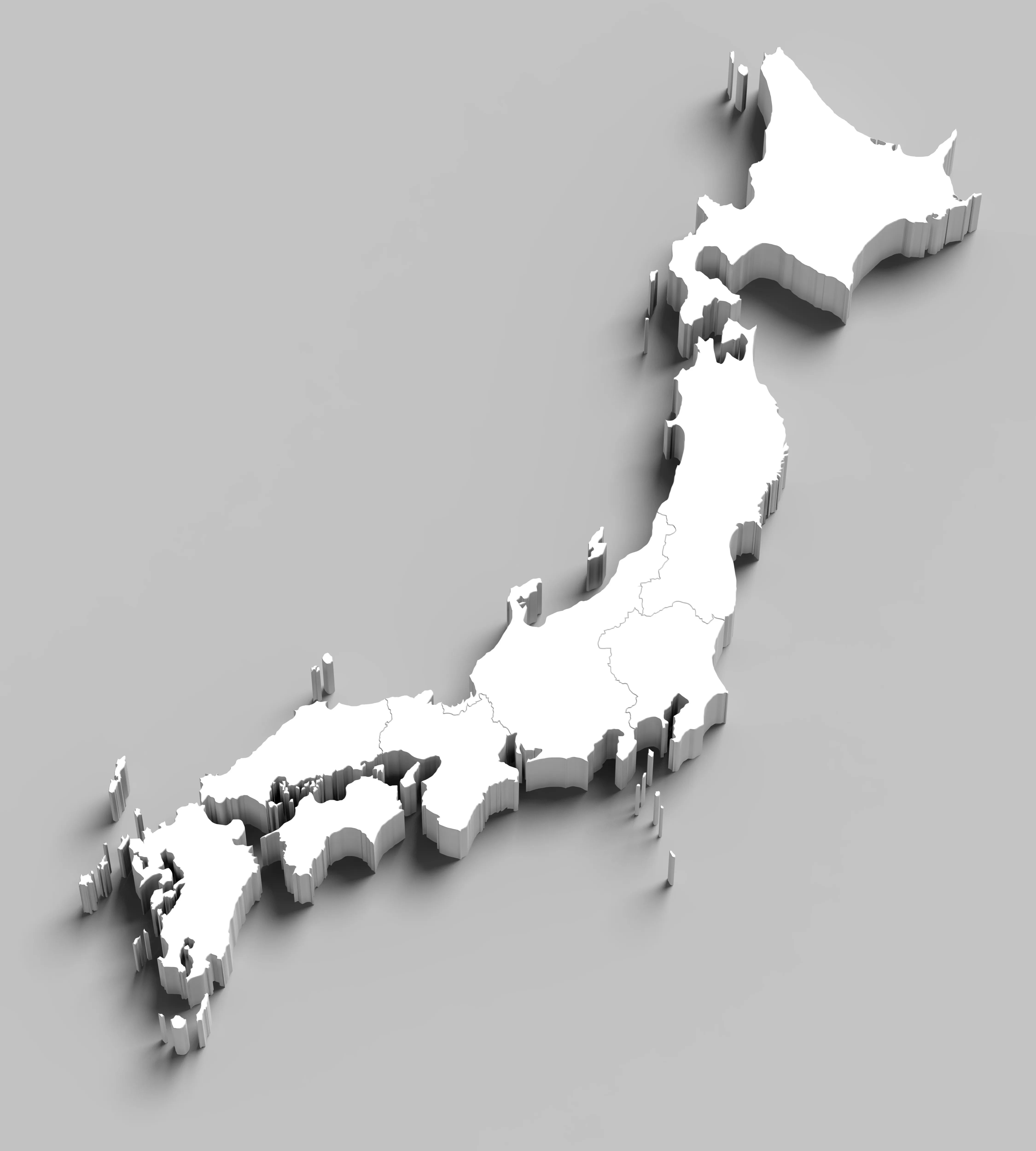
Kyushu, the third largest island in Japan, is home to the semiconductor production bases of integrated device manufacturers (IDMs) with world-class cutting-edge technology. SONY, Toshiba, Hitachi, Mitsubishi, Fujitsu and Nissan are among the sector’s shining stars, though a host of other IDMs tied to the supply chains of other major enterprises have also set root in Kyushu. Collectively, the companies earned Kyushu the name Silicon Island of Japan.Kyushu’s flourishing IDM industry sprouted from favorable tax and other government policies that reduced semiconductor production costs to levels lower than elsewhere in Japan. Once the IC producers had established bases, equipment and materials companies naturally followed, leading to the influx of many parts manufacturers. Together, they came to Kyushu, one after another, to make the island a magnet for manufacturing. And so it was to Kyushu that a SEMI China delegation travelled for a meeting at TEL’s factory in Kumamoto to learn more about the secrets to the rapid growth of the island’s semiconductor industry and promote cooperation between Chinese and Japanese enterprises. Underscoring the rise of the Silicon Island of Japan, China will soon become TEL’s largest market, said Masami Akimoto, Chairman of Tokyo Electron Kyushu Limited, speaking at the event. Masami Akimoto hopes for support from SEMI China.The island of 12 million people contributes to the growth of the global semiconductor industry, expected to reach USD 500 billion in size in 2019 as China’s semiconductor sector, fueled in part by government-backed investment funds, continues its rapid expansion. Despite the gains, China still lags other regions in advanced manufacturing, said Lung Chu, president of SEMI China, which is doing its part to draw more advanced manufacturing to the region through its SIIP platform. The initiative encourages pan-regional cooperation with China’s semiconductor industry to promote free trade, open markets, technology innovation and IP protection – all to help China better integrate with the global semiconductor industry. SEMI China President Lung Chu(L) issues visit memorial to Masami Akimoto(R), Chairman of Tokyo Electron Kyushu Limited. Chicken shall be led by the HenUnlike other regions with comprehensive semiconductor industries, Kyushu’s is primarily focused on production and assembly, with more than 200 manufacturers of semiconductor equipment and parts.SEMI China Delegation at Tokyo Electron Kyushu LimitedTEL built its first factory in Kumamoto, a city covered by volcanic ash in the center of Kyushu, 34 years ago. Today, TEL every month produces 80 to 90 sets of equipment, each consisting of, on average, over 400 thousand parts that must be certified and authorized by TEL before delivery to its module manufacturers and assembly into complete machines. Having blossomed over the past few decades, the island’s supply chain now supplies TEL with all its equipment parts. SEMI China Delegation at Fajita WorksTEL supplier Fajita Works, a high-precision plate metal manufacturer founded in 1945, is emblematic of other companies in the Kyushu supply chain. It keeps a low public profile as it serves several longtime customers and earns ardent loyalty from its workers, an ethos reflected in the change next January of its slog from “Only One” to “Great company, Great life.”Quality is the life of the enterpriseLong before the rise of its legendary automobile and consumer electronics companies, Japan was known for inferior, counterfeited products, labeled “Made In USA” and shipped to the United States by more than 100 factories. The net effect was to shrink and commoditize American markets. The tide in Japan’s product quality and stained reputation began to turn in the 1980s, when Japan’s semiconductor industry began to produce memory with an error rate 27 times lower than its U.S. competitors, giving Japan an upper hand in quality that it would never relinquish. SEMI China Delegation at HORIBAKyushu-based flowmeter supplier HORIBA, among the many Japanese companies famous for their product quality, ships 38 percent of its products into the automotive market and 27 percent into the semiconductor sector. Cleanliness is as vital a part of the company’s culture as quality. Each depends on the other, with fine detail held to the highest importance. On its visit to HORIBA, the SEMI China delegation, passing by an office area before entering the factory, sighed at the sight of the spotless, neatly kept furniture and workspace: They had never seen an office so sparkling clean. HORIBA’s success is rooted in immaculate offices, factories and the company’s motto “Enjoy innovation and pay close attention to product quality.”After Kumamoto sustained heavy damage during a 2016 earthquake, HORIBA workers returned rocks scattered by temblor to their original position, knowing that order is critical to lean, efficient manufacturing and that, indeed, “the devil is in the details.” SEMI China Delegation in Kumamoto City Full confidence in the exploration of Chinese marketConsumer electronics stalwarts Sony and Panasonic feature semiconductor factories in Kagoshima, the southernmost city in Kyushu and Japan, though rumor had it two years ago that Panasonic planned to pull out. The Panasonic plant, which provides batteries for Tesla, remains. The Sony facility produces image sensors for the iPhone.Semiconductor equipment maker ULVAC, SEMI China’s most important strategic partner, is also based in Kagoshima. During the delegation’s visit to the company, Lung Chu noted that while China is the world’s largest semiconductor market, the region meets just 13 percent of domestic chip demand. Stressing that ULVAC can play a crucial role in helping China become a bigger player, he expressed admiration for ULVAC’s professionalism along with hope that it will maintain its rapid growth and leverage SEMI resources to catalyze rapid development of Internet of Things (IoT), artificial intelligence (AI), and 5G technologies in China and rise into the top 10 of global equipment manufacturers. SEMI China President Lung Chu (L) issues visit memorial to ULVAC Kyushu President and CEO Kenji Yamaguchi ULVAC Kyushu president and CEO Kenji Yamaguchi made clear the company’s interest in Lung Chu’s insights into Chinese semiconductor industry while underscoring its core competency of producing semiconductors for flat panel displays. The Kyushu Factory of ULVAC is full of vitality and market competitiveness. SEMI China Delegation at ULVAC EBARA, a precision machinery company located in Kumamoto, has manufactured chemical-mechanical planarization (CMP) equipment for over 20 years and delivered nearly 2,400 mechanical polishing machines worldwide. While the company expects to ship 50 sets per year to China starting next year, it has the capacity to deliver 20 sets per month, enough to meet demand of Chinese semiconductor makers. SEMI China Delegation at EBARAThe most telling takeaway from the SEMI China delegation’s visit to the Kyushu: Japan ranks number one worldwide in research and development (R D) investment as a proportion of GDP and is also at the top in the percentage of R D funds controlled by private enterprises. The outsize investment strategy has enabled Japan to maintain its hold as one of the world’s top technology innovators.Like Sakurajima, the famed Kyushu volcano, the SEMI China delegation will continue to harness its forces to build relationships with the island’s semiconductor supply chain as it works to develop win-win pan-regional relationships and foster the growth of China’s semiconductor industry. Best view of Sakurai volcano Gang Yao is a marketing director at SEMI China.
Read More