downloadGroupGroupnoun_press release_995423_000000 copyGroupnoun_Feed_96767_000000Group 19noun_pictures_1817522_000000Member company iconResource item iconStore item iconGroup 19Group 19noun_Photo_2085192_000000 Copynoun_presentation_2096081_000000Group 19Group Copy 7noun_webinar_692730_000000Path
Skip to main content
Default Banner Image

semiconductor materials

Electric mobility, renewable energy and other technology innovations like IoT, 5G, smart manufacturing and robotics all require reliability, efficiency, and compact power systems, fueling the adoption of Silicon Carbide (SiC) and Gallium Nitride (GaN) to support lower voltages in significantly smaller devices. But chip designers must overcome the technological and economical challenges of integrating the two semiconductor materials into power systems.SEMI spoke with Elisabeth Brandl, Business Development Manager at EV Group about trends and new developments within the power electronics industry and the devices' application in smart mobility. Brandl shared her views ahead of her presentation at the SEMI SMART Mobility Forum, 18 February, as part of the SEMI Technology Unites Global Summit, 15-19 February 2021, online event. Join us to meet experts from EV Group and other key industry influencers. Registration is open. SEMI: What is driving new developments in power electronics?Brandl: Globally there are significant changes in infrastructure requirements for communication, automotive and power conversion. We need to look no further than the rising adoption of 5G, electric and hybrid vehicles, and renewable energy as examples of drivers of these changes. The device level, particularly in the field of power electronics, figures prominently in these shifts.The power electronics industry faces a growing number of scenarios where conventional silicon power devices are no longer suitable and are easily outperformed by new architectures mainly based on wide bandgap semiconductor materials like Silicon Carbide (SiC) and Gallium Nitride (GaN).SEMI: What industry challenges is power electronics innovation aiming to solve? Brandl: Power conversion efficiency is very important and needs further improvement as the related losses significantly contribute to the overall power consumption. For green power and a better environmental footprint, renewable energy is crucial, but so is overall power-consumption efficiency, yet the role of power devices is often underestimated. High-frequency and high-power applications, such as data center applications and inverters for renewable energy, where silicon power electronics are reaching their limits, are also important areas in power electronics.SEMI: How will the transition from silicon to compound semiconductor materials help?Brandl: The superior material properties of several compound semiconductors can tackle the need for lower losses in power conversion or better high-frequency behavior. Today, we mainly talk about GaN and SiC power devices as they are materials well-suited to address these needs. However, other materials like diamond and gallium oxide are in development for these applications. Material properties of SiC that enable thinner materials with lower power losses and better thermal behavior address power conversion efficiency as well as form factor challenges. GaN, especially in a high electron mobility transistor (HEMT), can be used for high-frequency applications.SEMI: What enables a better and more cost-effective manufacturability of SiC and GaN power devices?Brandl: For the end customer, a typical figure of merit regarding the cost effectiveness is $ per Ampere or Watt. While this seems simple, the reality is of course more complex. It is important to understand the main cost contributors within the manufacturing area. For SiC, this is clearly the substrate cost. In my presentation, I will show a way to reduce this cost via wafer bonding. For GaN, epitaxy – a method for growing or depositing mono crystalline films on a substrate – is the critical parameter. And of course, yield has a very big impact on cost effectiveness too, which means that good process control including metrology is very important.SEMI: Many semiconductor companies are already transitioning to silicon carbide and gallium nitride. Can you give us an example of a success story?Brandl: All the big power device manufacturers have either acquired or developed their SiC and/or GaN power device technology, so they also see a bright future for these wide bandgap semiconductors in the power device market. The most prominent success story is STMicroelectronics with its SiC MOSFET power devices, which have been implemented by Tesla in its Model 3 vehicles since 2018.SEMI: What is coming next?Brandl: New materials for power devices are being explored, such as diamond and gallium oxide. For SiC, the trend is moving toward 8-inch substrates, which is the focus of the funded EU project REACTION under the coordination of STMicroelectronics. Cost reduction and substrate availability also play a big role. All major power device manufacturers have contracts to secure the supply chain for SiC substrates because material availability is the main uncertainty at this time. Finally, collaborations along the supply chain are crucial and generally beneficial for all parties, as development requirements are better communicated and prioritized.Elisabeth Brandl is Business Development Manager at EV Group. She received her master in technical physics from the Johannes Kepler University Linz, Austria in Semiconductor and Solid State Physics. Since 2014, she has been responsible for Product Marketing Management for temporary bonding and compound semiconductors at EVG. The SMART Mobility Forum is the digital platform of SEMI Europe’s Global Automotive Advisory Council (GAAC) for industry stakeholders along the automotive and electronics value chains, from Design, Semiconductor Equipment and Materials Suppliers to Automotive OEMs.Smart Mobility is one of four SEMI initiatives focused on building communities, content, and activities around critical and emerging electronics markets. Read more about our Regional Chapters.Serena Brischetto is senior manager of Marketing and Communications at SEMI Europe.
Read More
Linx Consulting and Hilltop Economics continue to monitor how the global economy impacts the electronic materials supply chain. Amidst the recent economic and revenue results releases, we have generated a series of potential scenarios for the next few years. These scenarios are based around sales of silicon wafers expressed in millions of square inches (MSI). Our work develops a multiyear forecast from the historic record of the SEMI-reported MSI demand by developing an econometric relationship with underlying demand drivers. Using this methodology, Linx Consulting and Hilltop Economics have introduced the following three silicon demand forecast scenarios: V-shaped global recession consistent with severe COVID-19 impact followed by a sharp economic rebound. Probability of approximately 40%. V-shaped global recession but with business and consumer behavior differing from the past recession in that there is much more aggressive spending on technology goods that softens the impact for semiconductors in 2020. Probability of approximately 25%. An extended COVID-19 impact developing into a U- or L-shaped global recession with an economic rebound delayed for several years. Probability of approximately 35%. In the few months since coronavirus hit the world, the economic prognosis for all major economies has worsened dramatically, although forecasts remain speculative given the rapid rate of change in the political and economic environment. The forecast changes in GDP since February 2020 of the G7 nations vary from -5.9% for Japan to -10.2% for Italy. These changes are closely linked to unprecedented declines in employment, consumer demand and industrial investment – all key drivers for wafer area demand. This leads us to believe there will be a significant reduction in wafer demand as these economic factors feed through the supply chain.Other leading indicators show dramatic drops in the global and regional economies taking effect at an unprecedented pace. These indicators have a loose predictive relationship for silicon wafer consumption and portend a rapid drop in demand.The demand picture for the semiconductor supply chain (be it wafers, materials, consumables or devices) is thus gloomy, and our models are currently showing Q2 to Q3 2020 reductions in MSI demand of between -11% and -28% depending on the scenario.In marked contrast to this depressing economic picture, the indications from the end-to-end semiconductor supply chain continue to be much more positive. Demand for silicon reported by SEMI increased in Q1 2020 by close to 3% from Q4 2019, while results from materials supply companies vary from slightly negative to record-breaking growth rates through the first three to four months of 2020. Added to this, reported revenues from WSTS for Q1 2020 ticked up 6.2% versus the prior year and the three large foundries in Taiwan and China showed continued growth of Q1 wafer area shipments and a 32.3% growth versus Q1 2019.Revenue and demand reports from leading device manufacturers remain on trend from 2019 with no indication of a precipitous change. Anecdotal reports of strong technology equipment demand to support people working from home and demand for medical devices in response to the pandemic can be substantiated somewhat by demand data although not convincingly.Reports from materials supply companies indicate that factories continue to be fully utilized, having been designated essential businesses, and that safety measures implemented against infection are largely effective.There are some indications of caution, however. The major public silicon wafer suppliers saw a 4% drop in revenues in Q1 over Q4, despite the reported strength in silicon area shipments from SEMI, indicating either ASP declines or some inventory effects.We are advising clients supplying materials into the wafer fabs and packaging supply chains to develop contingency plans for a sharp decline in product demand of as much as 28%, which may bounce back rapidly to 2019 levels or higher in early 2021. However, companies should also be vigilant of a slower than hoped for return to previous activity levels if the effects of the pandemic continue for an extended period.For further information please contact Mark Thirsk at +1 774-245-0959 or on [email protected] in engaging with the electronic materials supply chain? The Electronic Materials Group (EMG) is a SEMI technology community representing SEMI member companies that provide substrates, polymers, metals, organic and inorganic materials, chemicals, and gases developed for electronics manufacturing. Linx Consulting is a longtime member and supporter of the SEMI Electronic Materials Group.Mark Thirsk is managing partner at Linx Consulting. Duncan Meldrum is president of Hilltop Economics.
Read More
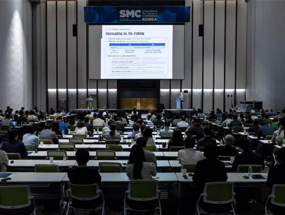
The semiconductor industry is in the final throes of its most recent cyclical downturn, but clear demand drivers on the horizon, such as 5G and autonomous driving, have created a decidedly upbeat mood at SEMI’s Strategic Materials Conference, held this week in San Jose, California. Increased connectivity in daily lives will not only dramatically boost semiconductor volumes, but the physical challenges of improving chip performance have positioned materials as the key enabling technology of the fourth industrial revolution – creating opportunities for suppliers to capture significant value. Most speakers were quick to underscore the importance of materials innovation. According to Dave Anderson, president of SEMI Americas, “We are entering the era of the material scientist,” and the role of materials in semiconductor manufacturing “has never been more important.” Carlos Diaz, senior director, corporate research at foundry major TSMC, said that the future “belongs to new materials and processes,” while Bertrand Loy, president and CEO, Entegris, told attendees the world is on the brink of the fourth industrial revolution, where technology will be fusing “physical, digital, and biological worlds and transforming our collective lives.” Len Jelinek, senior director/semiconductor manufacturing, IHS Markit, noted that 2019 has been a challenging year for semiconductor revenue – expectations are for a 12.5% decline YOY – but said he is not forecasting “doom and gloom” because of positive consumer demand trends beyond 2019. These include the rollout of 5G networks, internet of things (IoT), artificial intelligence (AI), and autonomous vehicles. Jelinek emphasized the foundational impact of 5G in particular. “Don’t think of 5G’s impact only in terms of handsets. It’s an enabling technology that will have broad-based impact” and will be key to creating a sustainable recovery in semiconductor demand in the second half of 2020. The current semiconductor downturn – the industry’s 10th – was initiated by an imbalance in memory supply and demand, and the lack of resolution of trade issues between China and the US is threatening to amplify volatility. Smartphones, the number-one application for semiconductors, are currently challenged by extended replacement cycles, and total handset shipments are set for its second year of decline. “We, as consumers, are waiting for revolutionary features such as 5G speeds, biometrics, foldable handsets and AI capabilities,” Jelinek says. Recent iterations have been merely evolutionary, and premium handset costs have escalated, he adds. Automotive electronics, which account for about 10% of global semiconductor demand, will eke out slight growth in 2019, Jelinek says. “Long-term semi component revenue growth within the Auto segment will focus on increasing content within cars supporting advanced safety features.” During his session, Duncan Meldrum, chief economist and founder of Hilltop Economics, addressed recent threats of a recession. “Underlying economic fundamentals are strong, but we are at that point in the business cycle where it doesn’t take much to knock the economy into recession,” he says. “I am telling people to have a contingency plan in place.” Nevertheless, Meldrum laid out reasons for optimism. Most economies have plenty of jobs, and consumers have been confident despite negative headlines. “For the average person, a tariff trade war gets to be noise. If they don’t see immediate impact, they tend to eventually discount all the headline noise. The same goes for Washington politics or Brexit.” There are no serious signs of inflation pressures in the US or other major economies, he adds. Beyond the cycleLonger-term, explosive growth in connected devices will create a runway for semiconductor volume growth. According to SEMI, over 30 billion devices are currently connected and another 200 million are added daily. By 2020, the number of connected devices will reach 1 trillion. “The growth profile for industry will be very strong and a multiplicity of drivers will bring more stability to this industry,” Loy adds. “But before this future becomes a reality we have a lot of work to do.” Current chips need to be faster and cheaper. “Physical scaling is not going to get us there, we’ve hit those limits,” Loy adds. “We have to look at new architectures and materials.” Loy called on the materials sector to need to “up our game” and spend more on R D. “Customers want us to make our products in very tight process window and ship to control. They want extreme purity for everything. It’s a long list of to-dos and it’s going to cost us a lot,” he adds. Among the needed innovations are photoresist hard masks to hand high aspect ratio, new etch chemistries for better rates and higher selectivity, and new cleaning chemistries for high aspect ratio geometry with high selectivity.Loy also identified contamination control as a key challenge for material suppliers. “When you think about purity and contaminants, you need to think about size, concentration levels, and classes. To optimize yields and lower wafer defectivity, our customers expect materials to be very pure and exhibit low variability.” The payoff for customers is large; a 1% yield improvement can mean $150 million in annual net profit for a leading-edge logic fab, Loy says. For a 3D NAND fab, that figure can be around $110 million per year. But these requirements are getting exponentially tighter. From 28 to 7 nm, the metal impurity concentration limit became 1,000 times lower, Loy notes. Contamination control is even more vital when the potential impacts of latent defects – which are difficult to detect in a fab and during electrical testing – are considered, particularly in emerging applications like autonomous driving, Loy says. “The cost of yield loss is expensive, but failure in a critical optical sensor of a car could be significantly greater, in terms of recalls or even human loss of life.” To meet tightening purity requirements, Loy recommends throwing out traditional thinking about contamination control. “In the past, we could get away with simple filtrations,” he says. “That’s no longer going to work. We need to collectively, up and down the supply chain, migrate to better filtration and purification and also rethink chemical delivery systems and packaging solutions to preserve the integrity of our products.”Metrology will also be key, but analytical capability is lagging. “We all like to believe that we cannot control what we cannot see, but that is exactly what we have to do.” The need for innovation is also being felt at the wafer level. Kevin Light, director, Applications Technology Americas at Siltronic Corp., said that as semiconductor markets become more diversified, silicon suppliers must recognize the distinct challenges each segment faces. Better wafer properties are required for next-generation chips, he adds. “Excessive wafer geometry can cause errors during lithography, especially when printing even smaller linewidths,” he says. The end result can be defocus and placement errors. When dealing with “More than Moore” architectures, wafer requirements are driven by other factors than defects. “More than Moore applications do not benefit from scaling, but instead drive capabilities of separate silicon parameters,” Light says. “In some cases you need high doping, in others the doping needs to be precise.” Czochralski crystal growth is suitable for high dopant levels, but the concentrations vary at the top and bottom of the ingot. Float Zone crystals avoid oxygen incorporation and provide consistent doping. These variations make Czochralski process suitable for PowerMOS, and Float Zone appropriate for IGBT. Compound semiconductor layers, such as GaN-on-Si, offer potential advantages owing to higher switching speeds and critical breakdown fields, he adds. “Silicon wafer requirements are diversifying as the devices themselves find increasing use outside of traditional logic,” Light adds. “Moore’s law is alive and next-gen computing will continue to push the limits of flatness and cleanliness. Meanwhile, demands of energy efficiency, electrification, IoT, and 5G drive wafer requirements other than scaling, including extremely high doped or ultra-low oxygen growing techniques, high lifetimes, and substrates engineered for compounds semiconductors.” Driverless futureAutonomous driving was a frequent discussion topic at SMC. Although IHS Markit does not see it really rolling out until past 2025, the disruption to the auto industry’s status quo is very much being felt now. Dragos Maciuca, executive technical director, Palo Alto Research and Innovation Center at Ford Motor Company, says cars of the future will be autonomous, connected, electrified, and shared. “The biggest transformation will be the shift from mechanical hardware to software,” he says. “Currently [a car] is a mechanical thing that has some electronics. Going forward, it will be a software-driven system that happens to control some mechanical elements.” The transition is already way under way, so much so that autonomous technology developed for the automotive industry is already being spun off into other sectors, such as mining and agriculture, and the auto industry’s competitive landscape is already seeing changes. OEMs and carmakers are entering the market from the traditional auto industry side, while companies such as Google are participating from the software side. “Others, like Uber and Lyft, are coming in from the business plan point of view to eliminate drivers and improve margins,” Maciuca adds. Autonomous driving will require numerous innovations, many of which will require new electronic materials and production processes. “We need weight savings, space savings, and advanced architecture,” Maciuca says. “We also need customization to print circuits as the vehicle comes down the line.” The tech community is proving up to the task. For LIDAR, there were just two technologies available a few years ago, he adds. The impact on chipmakers is also already being felt. “The automotive industry used to buy older chips,” Maciuca says. “Now we are moving to a stage where we need the very first chips at the most advanced node. And we are using them for safety-critical operations. If an AI chip that is supposed to detect a human fails, the consequences can be very severe.”Rebecca Coons is a senior editor at Chemical Week. Republished with permission from Chemical Week.The SEMI Electronic Materials Group (SEMI EMG) is the backbone of the Strategic Materials Conference. EMG is a technology community representing SEMI member companies that provide substrates, polymers, metals, organic and inorganic materials, chemicals, and gases that are developed or in use for the manufacturing of electronics. The group is open to SEMI Members involved in materials manufacture, distribution, and services throughout the microelectronics industry. For more details, please visit the website.
Read More
SEMI spoke with Antoine Amade, Regional Senior Director EMEA at Entegris, about the challenges set by the car industry, and the concept of “zero defect” and the need for a collaborative approach ahead of his presentation at the Strategic Materials Conference at SEMICON Europa 2018, 13-16, November 2018, in Munich, Germany. To register for the event, click here.SEMI: The automotive industry is setting new challenges. This is very exciting source of growth for the global supply chain, but what are in your opinion the automotive requirements of the future?Amade: By 2030, 50% of the car cost will be electronics related. With the autonomous cars, there will be no tolerance for any type of chip defects because it will have a direct impact on human safety. With that in mind, higher reliability, increased efficiency and control across the supply chain will be the main requirements of the automotive industry.SEMI: Is the New Collaborative Approach the solution to overcome the challenges related to the automotive requirements of the future such as defects and contamination? What can you tell us about this approach?Amade: The automotive industry presents a great challenge to all of us, reaching the ppb level in terms of defectivity. In other words, this zero defects objective requires a collective awareness and understanding: Within an aging and more complex manufacturing environment, we all need to challenge the status quo and go for a new collaborative approach.SEMI: What does Entegris propose?Amade: We trust that contamination control has a major role to play to reach the zero defects. We are now in the 3rd generation of contamination control. After the focus on the cleanroom environment and equipment, materials are now at the center of the attention. With Entegris offering the broadest portfolio in terms of advanced chemicals, filtration and purification, and materials handling, we’re uniquely positioned to address precision, purity, integrity, and safety challenges.SEMI: How could this support fab managers in their daily challenges and mid-term future objectives?Amade: The new collaborative approach is a journey. It is a consultative process to provide a fresh set of eyes and expertise on the key areas of concerns in the fabs. It is a multidisciplinary approach with zero defectivity as the main goal. It is focused on base line improvement, better process control, more uniformity and prevention of excursions.SEMI: What do you expect from SEMICON Europa Strategic Materials Conference?Amade: It's the perfect platform to deliver our message in front of the whole ecosystem. It obviously concerns the fabs, but also material suppliers, and even carmakers. We expect this new view of collaboration will create an engagement from all parties. It is not a coincidence that this is called New Collaborative Approach. Antoine Amade joined Entegris in 1995 as an application engineer in its semiconductor business. In his current role as EMEA Sr. Regional Director, Mr. Amade manages a sales, customer service and marketing team responsible for growing the semiconductor business in Europe and Middle East.Mr. Amade held leadership positions at Entegris including gas microcontamination market management, strategical account management and regional sales management. He has a degree in Chemical Engineering from ENS Chimie Lille and is a member of Semi Electronic Materials Group for Europe. Serena Brischetto is a marketing and communications manager at SEMI Europe.
Read More