downloadGroupGroupnoun_press release_995423_000000 copyGroupnoun_Feed_96767_000000Group 19noun_pictures_1817522_000000Member company iconResource item iconStore item iconGroup 19Group 19noun_Photo_2085192_000000 Copynoun_presentation_2096081_000000Group 19Group Copy 7noun_webinar_692730_000000Path
Skip to main content
Default Banner Image

manufacturing

Presentations from SEMICON West’s “The Convergence of Semiconductor Manufacturing and Design” offer great insights into the collaboration between the two, as I was recently reminded by presenter Sutirtha Kabir, R D Engineering, Executive Director at Synopsys.Reviewing his talk “Revolutionizing Silicon to Systems Design: Unlocking the Future with 2.5D and 3D Multi-Die Innovations” was a good kick-off for our discussion that covered the continuous need for collaboration and where AI fits. Kabir, as I quickly learned, is a technical innovator and articulate communicator passionate about ongoing collaborations between design and manufacturing. Today’s blog post is the second in a four-part series featuring presentations from the SEMICON West design program, organized by the ESD Alliance, a SEMI Technology Community. The first blog, with Dave Kelf, CEO of Breker Verification Systems, appeared on January 6 (“Circular Collaboration Leverages EDA Advances”).Smith: How do you define collaboration between design and manufacturing?Kabir: Multi-die design and advanced packaging are a big focus of high-performance computing (HPC) and AI chips. Engineers are trailblazing and foundries are coming up with new stacking combinations. For this reason, design and manufacturing teams need to be closer than ever. Solutions must be made available to give ample visibility to manufacturing from the very start of the design process. Single die design has been done for 15 to 20 years with a continuity of power, area, and performance (PPA). Design flows, methodologies and the ecosystem between design houses, EDA vendors and foundries are mature and stable. The conundrum is that it's a different situation with multi-die designs. Not only is multi-die emerging rapidly, but the types of design innovations are different.We have been working closely with our foundry partners to move multi-die innovation forward by enabling more advanced process and packaging technologies. I don't see this slowing down as they are coming up with different ways of doing designs. Design teams are collaborating closely with the foundries to take advantage of the benefits of these new multi-die designs.Smith: You mentioned new stacking combinations and collaboration with the foundries. What about collaboration with the OSATs? Kabir: Generally, it’s both silicon foundries and OSATs. With advanced packaging, both play a significant role depending on the types of applications being targeted. Design house targets may shift from the traditional silicon foundry to several OSATs. For example, if an organic interposer is required, the collaboration could be with an OSAT in conjunction with the silicon foundry. There are many possible collaborations that may be required. The point I’m trying to make is that there is a strong need for collaboration between EDA and the foundries during design that continues through manufacturing and test.Smith: What trends in general are driving the need for this collaboration?Kabir: The trends are performance and scalability and the need for high-performance compute. Look at some of the mega-chip systems coming out today compared to the bigger systems from five years ago. HPC was not driving that much in 2.5D. The big interposers used to be on silicon, maybe 1.2 to somewhere around less than three reticle sizes. Today, the reticle limit is more than 5X. Leapfrog to today, and the configuration has changed where the state of the art is to use an organic interposer with multiple embedded bridges (up to 20 or more) buried inside the interposer to support high-speed interconnect. The organic interposer with multiple layers on the front side and back side communicates with bridges and the SoC and HBM that sit on top of that interposer.3D architectures stack dies with GPUs and a large amount of HBM such as an HBM4 memory stack. The memory stacks may be 8 or 16 high. All of this memory needs to be as close as possible to compute for scalability. In terms of the high-power demand, the designer needs to make sure that the voltage that is pushed from the bottom of the stack can feed the power hungry SoC blocks on top of the 3D stack. At the end of the day, EDA is all about giving design and manufacturing houses the capability to predict how a design is going to perform in all different kinds of scenarios. EDA must keep up with this trend and that requires collaboration.Smith: What about the verification side, specifically system verification? Kabir: Let’s say I am using a spreadsheet and doing back-of-the-napkin calculations, a technique that used to work well for single die or design blocks. Multi-die doesn't scale since multiple heterogeneous dies in a single package must be considered. Design planning must include directional changes to measure the effects with key performance indicators. The challenge is to correlate signoff and verification. Signoff engineers can no longer just verify at the end of the design cycle. Instead, it has become a continuous process that transcends the flow from design planning through implementation and signoff and release to manufacturing.The industry is repeating a pattern from about 20 years ago, when single-die design evolved from relatively naive approaches to much more sophisticated EDA-flow-driven methodologies.Smith: As you drive the tools forward, who are your counterparts on the manufacturing side? Kabir: It depends on the different stages of design—design planning, implementation or signoff. It starts at the architecture stage from the left when architects and physical design engineers are doing floorplanning. The term design technological co-optimization (DTCO) has evolved into S (system)TCO now because we are trying to co-optimize system design and technology. I'll give you a simple example. A working chip manufactured in a certain technology node is going to be used in a multi-die design. Is the existing chip technology good enough to support the design or will it require a new chip at a different node? In either case, how does an engineer work with the manufacturing house to make sure it has the right metal layers or a different number of metal layers or a different metal width or some other property on the technology side? Designers need to make data-driven decisions based on the configuration and technology numbers to meet power budgets.In the past, what was once managed through designer-ASIC house-manufacturing interactions are now increasingly being handled by EDA flows as part of design implementation.Smith: Ultimately, it's driven by business. The hard work and decisions are made by two teams of knowledgeable technical people who must come together.Kabir: And then of course it has to be rolled into program management, business development and all this needs to be supported by data. We all recognize that the design window is not increasing. It’s always about trying to get more out in less time with less people. That doesn't help the equation.Bob Smith: How does AI fit into this and how is it best leveraged? Kabir: I’m hearing, learning, and reading about the tremendous advantages AI could bring. AI has a huge role to play, but it won’t eliminate the need for savvy design and verification engineers.Multi-die design brings together different users from different tool backgrounds. Even the language between a packaging person and a silicon person is different. The terminologies they use are different, as are the ways they have done design over the last 15-20 years. The same applies to thermal, power or signal integrity engineering. Bringing them together requires that EDA will provide platforms where the whole system design, including chip design, is managed. That’s a tall ask for people from all different backgrounds to come in, learn different technologies and tools within a short time. This is where ChatGPT or Microsoft’s Co-Pilot can be applied in the EDA world today to quickly find solutions by reading through manuals, application notes, forums and the like to find solutions. This use of AI agents can save tremendous amounts of time for designers. Another aspect that can be positively impacted are roles. We have customers coming to us and brainstorming on the use of workflows and methodologies, instead of the design aspect. Scalability from the human perspective has become difficult because of the need to closely guide engineers to get them up to speed on new technologies and workflows. This is where Agentic AI can deliver a huge productivity boost. It's not replacing anyone. It's getting them to decisions and end results faster.Smith: Can Agentic AI play a big role? Kabir: Current AI is like the person who, when asked a question, has to give an answer even if it’s the wrong answer. The same thing is going to happen when we bring in all these EDA technologies with AI capabilities.The point I'm trying to make is how do we verify that AI is doing the right thing? In EDA, one of the biggest questions and concerns is if a result or outcome or design can be verified. If it can't be verified accurately, verification engineers will not trust what AI is telling them no matter how fantastic the algorithm is. The verifiability of AI solutions is important for EDA. The key question is: Why would I trust what your tool is telling me to do?EDA flows that are more mature rely on decades of expertise, thorough documentation, and various scenarios to train AI algorithms. Those are the AI-powered EDA flows that I trust the most. About Sutirtha KabirSutirtha Kabir, an Executive Director of R D for Synopsys’ 3DIC Compiler, has over 20 years of product engineering experience, driving, building, and inspiring teams across companies in the EDA industry. In his role at Synopsys, he supports construction and analysis of multi-die systems including stacked ICs plus Interposer configurations. Prior to joining Synopsys, Kabir was a Group Director of Engineering at Cadence. Kabir has a Master of Science degree in Electrical Engineering. Robert (Bob) Smith is executive director of the ESD Alliance, a SEMI Technology Community.
Read More
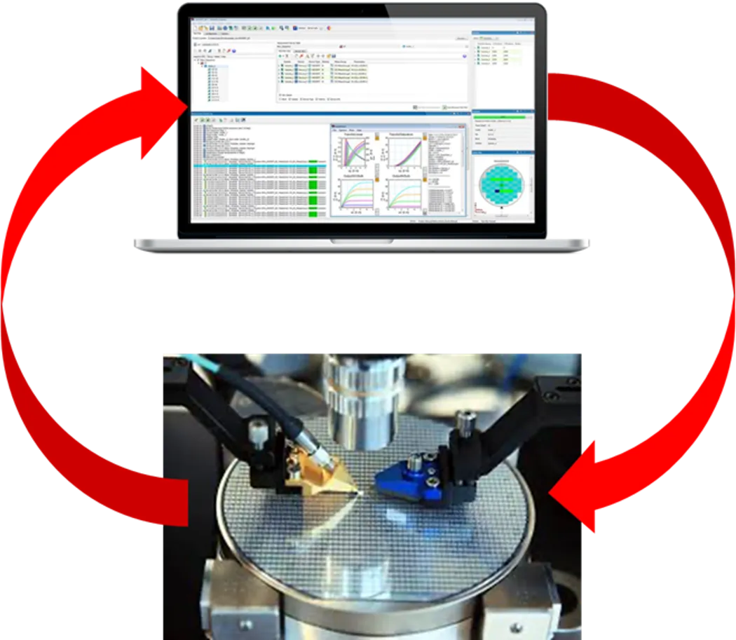
The SEMICON West 2025 design program “The Convergence of Semiconductor Manufacturing and Design,” organized by the ESD Alliance (ESDA), a SEMI Technology Community, featured presentations about successful collaborations between the design and manufacturing markets. The three-hour program in a packed conference room included plenty of great material that we’re using as the basis for a blog series that you will see over the next several months. I’m working on them now based on my conversations with four of the speakers where we discuss key drivers behind the need for collaboration and what’s ahead.I’m starting with Dave Kelf, CEO of Breker Verification Systems, a company steeped in front-end chip verification, who describes an actual circular collaboration that effectively leverages AI and other electronic design automation (EDA) advances. We recently talked about collaboration, integrated design and manufacturing flows and AI.Smith: How does Breker define collaboration between design and manufacturing? Kelf: In general, at a technical level, we would define this collaboration as the sharing of data, methodology and/or information that improves both processes. As semiconductors become more complex, this sharing process is increasingly important to effectively manage the overall complexity of today’s chip designs.Smith: What trends are driving the need for this collaboration?Kelf: Apart from the ever-increasing size and density of semiconductors, there are specific trends that require more interaction between design, verification and manufacturing. Obvious developments include the advent of chiplets, given the changes in performance of signal paths, and 3D devices driving complex packaging, power dissipation and other issues. Design issues such as the increased need for SoC coherency testing and complex device structures such as multi-core processors, also play a role. With many of these issues, design and verification (D/V) trade-offs have an impact on manufacturing, and vice versa. For example, differing delays on a Universal Chiplet Interconnect Express (UCIe) interface—an open specification for a die-to-die interconnect and serial bus between chiplets—will have an impact on hazard testing in coherency verification. As another example, thermal hotspots on some parts of a chip package might need additional testing during the verification phase. Smith: What trends and challenges are preventing a fully integrated design and manufacturing design flow?Kelf: Traditionally, the D/V and manufacturing teams have remained separate in most organizations, as well as between the two industries. EDA companies sell primarily to the design teams, although they do interact with the foundries at the back end of the process. Manufacturing companies work directly with different teams at the foundries and not with the D/V teams at all. New relationships need to be built up. The general know-how in these disciplines is different, and methodology approaches tend to be disconnected. The tradition is to separate the processes and use standardized interfaces for communication that leaves little room for improvisation. All this needs to change so that teams can begin to work more closely.Smith: What is circular EDA-manufacturing collaboration and vertical integration?Kelf: In past EDA flows, we have seen disparate tools performing specific functions. As semiconductors got smaller, their physics changed and this led to the design process absorbing new characteristics. For example, abstract designs were run through synthesis to create gates connected by wires. This format was then passed to place and route (P R) tools that would lay out the gates in terms of transistors and interconnects on the silicon wafer. On large devices, the gate level signal delays were larger than the interconnect, allowing design to be separated from layout. As silicon became denser, the interconnect delays became the dominant factor, and the layout of the device impacted the design synthesis process. The two tools required forward integration—synthesis projected layout rules to P R, and a reverse integration where layout characteristics were sent back to synthesis for redesign where required delays could not be handled during P R. The methodology went from a simple flow to a circular design approach as synthesis and P R cooperated. The same is now true of design and manufacturing where solving the problems noted above requires this same circular cooperation. Smith: What will it take to have an integrated design and manufacturing flow?Kelf: A lot of cooperation between different groups. As we reach limits in areas such as signal integrity and thermal management that will squeeze silicon efficiency improvements, these methodology linkages will be required for continued progress and growth. The industry (both design and manufacturing) will be highly motivated to make this happen. Smith: From a personnel perspective, who (on both sides) are the typical touchpoints? Kelf: It will be the engineering staff from both the design side and manufacturing that work closely to develop technical solutions. Executive-level support is, of course, needed to cement the collaboration. Smith: Where does AI fit?Kelf: AI will have a role to play in this. Estimating the factors that drive efficient design to manufacturing to design flows is a critical step in speeding interaction and providing sensible estimated starting points. AI can process the large amounts of data necessary to provide these estimates as we now see complex chips that contain billions of transistors. AI will be needed to accelerate the interactions for different tools through the development process.As design and manufacturing collaboration becomes a critically important industry strategy, companies are turning to SEMI and its Technical Communities such as the ESDA and their wide-ranging initiatives. For details and to get involved, visit the ESDA website at https://www.semi.org/en/communities/esda. To learn more about Breker and its solutions that provide test content portability and reuse to solve complex semiconductor challenges across the functional verification process, go to: https://brekersystems.com.About Dave KelfDave Kelf holds the position of CEO of Breker Verification after serving as its Chief Marketing Officer responsible for all aspects of Breker’s marketing activities, strategic programs and channel management.Earlier, he served as vice president of worldwide marketing solutions at formal verification provider OneSpin Solutions, was president and CEO of Sigmatix, Inc., and held senior positions at Cadence, Synopsys and Springsoft. Kelf holds a Bachelor of Science degree in Electronic Computer Systems from the University of Salford and a Master of Science degree in Microelectronics from Brunel University, both in the U.K., and an MBA from Boston University.Robert (Bob) Smith is executive director of the ESD Alliance, a SEMI Technology Community. 
Read More
The semiconductor industry is on track to expand and launch 97 new high-volume fabs online worldwide from 2023 through 2025, a major milestone that highlights the massive investment in chip production capacity. This rapid expansion is expected to drive a sharp increase in the deployment of pendulum valves. These valves, found in tens of thousands of semiconductor tools, are critical to the wafer manufacturing process.  Though hidden inside complex etch and deposition chambers, pendulum valves play a vital role in semiconductor manufacturing. They regulate gas flow and maintain the vacuum conditions required for precise wafer processing, ensuring efficient etching or deposition by controlling gases, managing exhaust flows, and maintaining chamber integrity. But what happens if a pendulum valve fails? It disrupts the vacuum necessary for wafer processing, causing chamber contamination and potentially ruining wafers. This leads to costly material scrapping, unplanned downtime, and production delays. Persistent failures can damage the turbo molecular pump or the entire tool, significantly increasing repair costs. Clearly, pendulum valves are essential for the reliability and performance of semiconductor equipment, particularly in etching and deposition chambers. Here are four critical reasons why:Consistent Vacuum Control: Maintaining a consistent vacuum environment is crucial for uniform layer deposition and etching, directly impacting the yield and performance of semiconductor chips. These valves regulate pressure and gas flow to ensure consistent and precise wafer fabrication processes. Contamination Prevention: Contaminants are a semiconductor manufacturer’s worst nightmare. Even microscopic impurities can destroy a wafer. Pendulum valves mitigate this risk with high-quality sealing mechanisms that create airtight environments, leading to high quality wafers and reducing waste.  Enhanced Yield: Pendulum valves are vital to achieving the highest possible yield in wafer manufacturing. Their ability to maintain operational stability and enhance process efficiency leads to fewer defects and higher productivity. By precisely controlling gas flows and preventing contamination, these valves reduce the likelihood of wafer defects and improve overall throughput. Minimal Footprint: Semiconductor fabs are high-tech, high-density environments where every square inch counts. Pendulum valves are designed with compact dimensions, allowing engineers to maximize production capacity without compromising performance or reliability.  Seal Performance Defines Valves’ Longevity  One of the core components of pendulum valves is its seals, directly impacting its durability, reliability, and maintenance. High-performance seals minimize downtime, reduce maintenance costs, and ensure a long operating life. However, achieving this performance requires attention to the challenges in semiconductor processes that impact performance and lifespan. Exposure to aggressive chemicals and plasma environments can degrade seals, causing erosion, sticking, and cracking. Continuous dynamic motion, including compression, decompression, and rotational movements, leads to friction and wear, shortening seal longevity. Errors, such as improper installation of static seals, can disrupt valve operation and cause delays. Extreme heat in wafer fabrication further tests the durability of valve components, while poor maintenance increases the risk of failures, resulting in costly downtime and repairs.  To keep valves operating at their peak efficiency, manufacturers need to prioritize five types of seals, identifying potential risks and tackling them effectively. The Pendulum Plate Face Seal, a dynamic component, must endure repeated compression and decompression during use. This constant motion, coupled with exposure to harsh chemicals, makes the seal vulnerable to issues like sticking and cracking. Without proper installation and attention, extreme failures, such as the seal dislodging entirely, can occur, disrupting operations.  Similarly, the Pendulum Plate Radial Seal performs a vital role, moving vertically within a piston bore. This component faces threats such as rolling, twisting, and chemical degradation, often leading to cracks or even fragmenting under severe torsional stress.   The Bonnet Seal, though static, is not exempt from potential difficulties. Improper installation or material cracking can severely compromise its functionality.  For dynamic applications like the Rotating Paddle Shaft Seal, friction is a constant adversary, compounded by chemical exposure that accelerates wear and tear.  Lastly, the Actuating Pins Seal, pivotal for enabling precise up-and-down movement within a piston bore, is particularly sensitive to installation errors.  When Failure is Not an Option  Addressing these challenges is essential to maintain the reliability and longevity of pendulum valves in semiconductor manufacturing. Greene Tweed uses a structured framework ‘Right Seal Pyramid’ to select the most suitable seal for every application. This process considers key factors like material compatibility, seal geometry, and operating conditions to develop solutions tailored to the specific needs of semiconductor manufacturing. By aligning seal types with precise engineering criteria, the Right Seal Pyramid methodology addresses key challenges like chemical resistance, mechanical stress, and installation accuracy, ensuring reliable performance in the harshest semiconductor manufacturing environments.  Explore MoreWant to learn how to prevent premature pendulum failure? Catch our full webinar replay or download our Semiconductor Playbook for expert insights, innovative solutions, and best practices tailored to your most critical applications. Carmen Quartapella is a Senior Engineer of Design Analysis at Greene Tweed. Quartapella has developed deep technical expertise over a three-decade career that spans multiple facets of the semiconductor industry. Throughout his career, he has gained expertise in Semiconductor Engineering, Engineering Management, Sales, Business Management, and Emerging Technologies. He graduated from Drexel University with a degree in Mechanical Engineering
Read More
As we move through Q2 of 2021, it seems that the world is finally approaching normalcy. But I don’t believe our lives and businesses will ever be the same. Travel is unlikely to return to the same level as pre-COVID-19 for many years. I’m sure many companies will establish tighter travel policies and budgets as virtual conferencing has proven to be beneficial and cost-effective. Patients and doctors who were skeptical of telemedicine are embracing it, and although it’s not perfect, it has filled a needed gap. Online learning essentially happened over a weekend and will now be part of many curriculums and programs. All of these elements have spurred our semiconductor industry into a super cycle. Demand for chips is leading to an increased demand for semiconductor equipment. Semiconductor capital equipment expenditures in 2020 surpassed $63 billion and are forecast to top $70 billion in 2021. The secondary equipment market typically makes up about 5% to 10% of that. Our inquiries have definitely increased this year. With this in mind, I’d like to share some thoughts for the remainder of the year. Storage of Chipmaking Equipment Not New The semiconductor industry has been experiencing an equipment shortage for some time. It is difficult for original equipment manufacturers (OEMs) to support such a large variety of products and technologies. Some companies use equipment for manufacturing 150mm, 200mm and 300mm wafers. Fabs still run 30-year-old technology on 150mm wafers while the latest technology is manufactured on 300mm wafers. We’ve also seen new technologies like silicon carbide (SiC) being developed on these smaller wafer sizes. Unfortunately, some OEMs stopped making 150mm and 200mm some time ago and have only recently jumped back into the market. These OEMs have had to balance technological advances, pricing, and manufacturing capacity to meet this demand since their primary focus is on 300mm equipment. Third-party refurbished equipment suppliers have also experienced an increase in demand over the last several years. We see it increasing at all technology levels over the next three to five years. This translates to increased equipment pricing for both new and used equipment, as well as increased lead times. Growing Demand for Legacy Tools Many electronic products we use and are familiar with don't require state-of-the-art technology. For instance, cellphones, electric vehicles, wearables, monitors and industrial products still contain many chips manufactured on 200mm wafers using 200mm equipment. There are still approximately 200 200mm fabs worldwide and this makes up about 25% of all wafer capacity regardless of wafer size. These fabs manufacture analog devices, MEMS products, power management ICs, RF devices, discrete devices and sensors. We have also seen an increase in lead times for 200mm equipment. Typical lead times of three to six months have increased in some cases to one year or more. This situation has created a dramatic increase in chip making equipment prices and we do not expect much relief there. Many OEMs transitioned to 300mm equipment prior to 2010. Revenue and profit margins are much higher for them on 300mm equipment. 200mm manufacturing was supported by many third parties for a while. However, in 2016 we saw a resurgence in 200mm equipment, and at that time many OEMs began jump-starting their supply chains. It took some time for them to develop new supply chains, upgrade technology and in some cases hire newly trained engineers to support these new tool sets. All this costs money, which is why we will continue to see an increase in new legacy equipment pricing. Because manufacturers and products may not be able to support these prices, we expect the robust third-party ecosystem to continue. SurplusGLOBAL's Response to this Demand One of the advantages we bring to the secondary equipment market is our ability to recycle technology. We continuously search for opportunities to purchase large packages of tools from companies that are transitioning technology nodes, moving from 200mm to 300mm wafer size or changing product lines. We spend approximately $65 million to $100 million each year on purchasing equipment and in some cases storing it for the right customer. For instance, a memory company may be changing technology nodes and no longer needs its equipment. This use to happen on a predictable schedule. Instead of scrapping that equipment, SurplusGLOBAL purchases and stores it. Sometimes we only need to store it for one month before relocating it. However, in many cases, we store it for one year or more. We may power it on at a later date if it is in good condition. In some cases, we work with an OEM or third party to have it refurbished and ready for a new customer. In response to the need for more secondary market equipment, we have opened up additional offices in Japan and Singapore to stay close to and better support our customers in those regions. Finally, our biggest and most recent endeavor is building our Semiconductor Equipment Cluster, which opens in July 2021. Learn more about the SurplusGLOBAL Semiconductor Equipment Cluster. Emerald Greig is executive vice president Americas at SurplusGLOBAL.
Read More
The evolution of industrial and non-industrial automation, smart manufacturing, and Industry 4.0 technologies have increased demand for vision systems that support robust, reliable imaging industrial applications. What factors are driving growth in the machine vision market today?SEMI spoke with Frederic Laune, Business Manager, European Technology, Corning, about how Corning® Varioptic® Lenses are vital to advancing the speed, efficiency, and integration of products using computer imaging. Laune shared his views ahead of his presentation at SEMI MEMS Imaging Sensors Summit, 25-27 September, 2019, at the WTC in Grenoble, France. Join us at the event to meet Corning and many other key industry influencing players. Registration is open.SEMI: Corning's markets include optical communications, mobile consumer electronics, display technology, automotive, and life sciences vessels. Back in June 2019, Corning Incorporated announced that it had delivered its 2 millionth Corning® Varioptic® Lens for industrial applications. What drove this great milestone?Laune: This milestone was met thanks to the fact that Corning Varioptic’s solution solves several problems generated by classical motorized solutions used in industrial applications: limited number of actuation cycles, poor vibration and shock resistance, size (meaning bulky), and high-power consumption. Before Varioptic, there was no variable focus solution that worked well.In addition, the explosion of the CMOS sensor technology helped drive down the cost of imaging solutions for industrial devices, increasing the number of applications and shipping volumes.SEMI: What inspired Corning Varioptic Lenses?Laune: Varioptic was started in 2002 by Dr. Bruno Berge, a French physicist turned entrepreneur. Inspired by the work of Gabriel Lippmann, the 1908 Nobel Prize winner for the invention of color photography, Dr. Berge explored the shape-altering effects of an electric charge when applied to two liquids, a phenomenon referred to as electrowetting. His research ultimately led to the creation of liquid lenses.Fast forward to 2017, when Varioptic became a part of Corning through an acquisition that included Varioptic and Invenios technologies. We believe the synergies from this acquisition will lead to exciting new liquid lens application opportunities that align with Corning’s growth strategy and core capabilities. Corning is one of the world’s leading innovators in materials science. For more than 165 years, Corning has applied its unparalleled expertise in glass science, ceramic science, and optical physics to develop products that transform industries and enhance people’s lives.SEMI: What differentiates traditional camera systems from adjustable lens solutions?Laune: Traditional industrial cameras are usually fixed focus, meaning that the image is sharp only in a limited distance range. Unlike consumer camera applications, there were no good solutions for variable or auto focus cameras in the industrial space. This is due to the intrinsic limitations of motorized technologies.Therefore, customers were using, for example, several cameras to focus at several distances. This compromises the optical quality by closing the objective in order to increase the depth of field, therefore limiting resolution and leading to a need for more light.The cameras using Corning Varioptic’s technology offer more functionality with their ability to focus, whatever the distance, in a fast, reliable, and accurate fashion, and with lower power consumption than traditional mechanical solutions. The upshot is that the product that can withstand heat, vibration, mechanical shocks, and high numbers of focus cycles in tough industrial environments. SEMI: And how is electrowetting enabling industrial devices to capture images and process information quickly and clearly? Laune: In two words: fast and accurate.Electrowetting has unique features – with our two-liquid solution, we combine fast focus with high vibration and shock resistance, and the added benefit of low power consumption.What’s more, our programmable lens can be reconfigured on demand. The lens adapts rapidly and continuously from diverging to converging and can be modeled to support demanding variable focus applications. Our lenses can change their focus in milliseconds, similar to the human eye, and capture fast-moving objects at varying distances. The use of liquid, over mechanical solutions, allows us to create a small form factor, saving precious space and reducing power consumption.SEMI: What industrial applications are taking advantage of this technology? Can you name one example?Laune: 2D barcode readers and industrial vision are our main markets. There is also a strong adoption of our technology in medical applications.SEMI: What does the rise of machine vision mean for manufacturers? Give us one prediction about the opportunities offered by advanced imaging applications.Laune: A great example is the use of 2D barcode readers and liquid lenses to track your ecommerce order, point to point. Another example is full product traceability by implementing a 2D barcode on every component of a given product globally to improve product quality. The varying and adjustable focus abilities of our liquid lens technology make it possible for barcode scanners to track products of different heights, allowing manufactures to improve their processes and logistics.Beyond these examples, tracking and analyzing are booming, thanks to the combination of low-cost CMOS sensor technology, increasing processing power, innovative algorithms (deep learning, AI, neuromorphic processors, etc.), and better image quality due to the progress of lens technology, Varioptic being one.We see an opportunity to improve people’s lives, such as enabling better analysis of medical images and improving the use of cameras in biomedical technologies.SEMI: Quality inspection and automation, adoption of Industrial 4.0 technologies, government initiatives. If you were to choose one, what main factor will drive growth in the machine vision market?Laune: It is difficult to pick just one. I believe that full traceability (monitoring individual parts throughout the production process) has interesting implications as compliance and regulatory efforts ramp up and stronger security of goods becomes more important, particularly as consumers become engaged in food safety and tracing products throughout the supply chain.SEMI: What are your expectations for the SEMI MEMS Imaging Sensors Summit and why would you invite your peers to attend? Laune: I strongly believe in the power of human interactions in technology and science! Ideas come from discussions and physical interactions. The SEMI MEMS Imaging Sensors Summit is a great place to network, meet people, and think about the future! Frederic Laune is the business manager leading the Corning® Varioptic® Lenses business. Laune joined Varioptic as an R D engineer in 2003 after spending the first eight years of his career developing novel active components for the optical telecom industry. At the time, Varioptic was a newly created start-up aiming to develop liquid lens technology for industrial applications. After designing the first two Varioptic commercial products, the Arctic 320 and Artic 416, Laune stepped up as head of Varioptic’s R D department to focus on product and performance improvements. In 2010, he was appointed sales and marketing lead for the company. Varioptic was acquired by Corning Incorporated in early 2017. Laune received a master’s degree in physics and optics from University Pierre and Marie Curie (Paris) in 1995.Serena Brischetto is a marketing and communications manager at SEMI Europe.
Read More
This article is the fourth in a series highlighting the vital importance of SEMI Standards to commemorate the publication of the 1000th SEMI Standard in July 2019. Find the entire series here.Computer prices have plunged over the years even as desktop and laptop PC performance has skyrocketed thanks to the semiconductor industry, giving users much more bang for their buck. The chip industry stands in a stark contrast to healthcare and education with their exponentially rising costs.What distinguishes the semiconductor industry from healthcare and education in the capacity to deliver so much for so much less over time? After all, even in other parts of the technology sector that are heavily regulated, such as cable television, we have not witnessed the same price decreases as in microelectronics.Some pundits claim that the difference among sectors is tied to their degree of regulation. Does greater regulation somehow degrade product value? The reality is far more nuanced. But one thing is clear: Smart self-regulation (i.e. standards) in the semiconductor industry has contributed mightily to its success.The recipe for success has been simple. Standards have been rocket fuel for competition, which in turn has sparked innovation, driving down device prices while boosting performance. Computer prices fell dramatically between 1997-2015 while the cost of cable TV and internet services rose. Myth of unregulated competitionA semiconductor fab might actually be the most regulated place on earth. Fabs hew to a much higher standard of air quality and cleanliness than even uber-sterile hospital operating rooms. Manufacturing processes are voluntarily regulated not to millimeters, but to nanometers. While some standards are proprietary with limited reach, others span the supply chain. Regulation has worked so well in this sector that the semiconductor industry isn’t moving toward less standardization. It’s moving toward more. Secret is smart standards The gap between regulation and self-regulation is more like a chasm. We typically view regulation as a series of top-down directives that more often focus on the interests of the producer than the consumer. Healthcare regulation, for example, may improve quality of care, but it’s often insurers, big pharma and hospitals that benefit most from regulation, rather than consumers.The semiconductor industry, on the other hand, uses self-regulation to improve business operations and make better products for consumers. Falling prices and rising performance are natural byproducts.Semiconductor industry self-regulation is an ecosystem-wide effort, where input isn’t just top-down, but also bottom-up or even side-to-side. The first SEMI Standard, which specified wafer sizes, exemplifies this approach.The SEMI Standards Committee formed in 1973 to address silicon wafer dimensional specifications. At the time, wafer specifications proliferated. Numbering more than 2,000, the various specifications led to major inefficiencies just when the industry was just getting underway. Wafer suppliers banded together under SEMI to solve this problem and rapidly developed consensus specifications for 2- and 3-inch wafers. By the mid-1970s, over 80% of wafers conformed to these new standards.Standardized wafer sizes freed equipment companies to focus on innovations that reduced cost and increased performance. It also allowed manufacturers to focus on product differentiation without having to worry about device fabrication process and cost. Since that first SEMI Standard made possible the modern semiconductor equipment industry, original equipment manufacturers (OEMs) have competed to deliver amazing innovations. For example, lithography systems routinely use light to design chips with feature sizes smaller than the wavelength of light.SEMI’s 1000th standard on energetic materials demonstrates how smart standards are also pragmatic. This standard is not about banning materials or assigning blame when things go awry. It is about creating practical guidelines that companies will follow, enabling them to realize greater innovation. Guidelines that reduce accidents and risks will spur more, not less, energetic materials’ exploration. Industry suppliers will be the big winners.The 1st to the 1000th SEMI standard all represent examples of cooperation making more sense than competition.Standards for the real worldCreating a business-friendly standard that still gets the job done is a process. As SEMI Standards Task Force and Committee members, materials, equipment and manufacturing companies take part in defining best practice guidelines that support safe and practical use of materials and equipment. Task force and committee members assign particular responsibilities and associated costs to the most logical segments of the supply chain. They also develop information-sharing practices around competitive process recipes and purity standards.Andy McIntyre, CIH, a member of the energetic materials task force and an executive vice president and managing principal at BSI EHS Services and Solutions, summarized what makes SEMI standards smart.“SEMI standards are pragmatic,” said McIntyre. “They take into account the need for implementation in a real-world business environment. They embrace an engineering approach to problem-solving to create practical solutions, and they define specifications and performance goals in ways that allow engineers — in collaboration with EHS professionals — to identify practical solutions for reducing risk in R D, pilot line and manufacturing operations.“SEMI standards employ a holistic process that considers all the important points of view throughout the supply chain, from materials selection, installation, use, recycling and/or disposal,” said McIntyre. “The breadth of SEMI EHS Guidelines, for example, is also very comprehensive as the SEMI EHS Committee and task forces work to ensure that standards keep pace with dynamic technology developments. Energetic materials is a prime example where the industry recognized the need for a new safety guideline to document safe usage of pyrophoric, water-reactive and unstable reactive materials, which have become increasingly important in semiconductor and advanced materials R D and manufacturing.”This is the real secret to the success of the semiconductor industry. Smart self-regulation allows industry players to cooperate in the development and implementation of standards that are pragmatic, comprehensive and dynamic. Participants in SEMI Standards have a voice in the semiconductor industry because they are the voice of the semiconductor industry.While innovation in semiconductors may not always keep pace with Moore’s Law, we can depend on one truth: As long as collaboration and cooperation are the rule and not the exception, we will continue to advance technology in amazing and unprecedented ways. You, me and all other consumers will continue to reap the rewards of innovation. Use your voice to affect standardization in and around the semiconductor industry. Learn about SEMI Standards – and become part of the solution.Heidi Hoffman is senior director of technology communities marketing at SEMI. Hoffman and her team shine a spotlight on the work of the more than 20 technology communities under the SEMI electronics manufacturing supply chain collaboration platform. Actively engaging community members in marketing programs that showcase their unique value, Hoffman’s team helps companies to grow and prosper through the power of connection, collaboration and innovation.
Read More
This article is the third in a series highlighting the vital importance of SEMI Standards to commemorate the publication of the 1000th SEMI Standard in July 2019. Find the entire series here.SEMI Standards are the bedrock of the modern microelectronics industry. Without standards for wafer dimensions – which SEMI Standards first defined through a collaborative process involving semiconductor manufacturers and wafer suppliers in 1972 – the semiconductor equipment industry as we know it would not exist today. The late Robert Noyce of Intel noted in this 1992 video “being good at producing semiconductors will mean we have better, more consistent, better controlled equipment than we have in the past. Standards are going to play a vital role in that. Standards saves money and time for everyone.” Noyce also called standards a bellwether to surges of innovation in critical process technology. This is still true today as, for example, important standards-setting activity is afoot in panel-level packaging, electron microscopy and energetic materials. Will a surge of innovation follow?Panel-level packaging: a chicken-egg scenarioFrom advanced materials to more efficient production tools, one hallmark of the microelectronics industry is our fearless exploration of new technologies that will spawn change across the industry by improving performance and reducing cost. Advanced packaging techniques, such as panel-level packaging (PLP) – which moves semiconductor packaging to a larger-panel format – is one of those critical catalysts. Citing PLP’s potential to shrink costs by improving efficiency and economies of scale, research firm Yole Développement predicts a remarkable 63% CAGR for PLP from 2017-2023.[i]It’s no stretch to say that we are close to realizing a burst of innovation in packaging. With a just-published SEMI Standard (SEMI 3D20) specifying panel sizes, equipment companies will find it economically viable to invest more in developing the much-needed production tools that enable PLP. “It is really important to create standards so we come together and work much more efficiently. Creating those fundamentals allows you to be more productive in the long term,” said Christina Chu, ASM Semiconductors, and co-leader of the Panel Level Packaging Task Force, and one of five industry leaders recognized for their outstanding accomplishments in developing SEMI Standards for the electronics and related industries at the recent 1000 SEMI Standards reception during SEMICON West 2019. “This effort came up from the trenches,” said Richard Allen, NIST Quantum Measurement Division, and a co-leader of both SEMI’s 3D Packaging and Integration Committee and its Panel Level Packaging Task Force. “Equipment vendors told us that they wanted to serve the market, but they couldn’t do so without some standards. To respond to their request, our committee surveyed the market and discovered at least 15 different panel sizes in development.”“As no vendor is going to make over a dozen unique tools for the same process, we worked with the manufacturers and tool companies to write a specification that standardizes on two of the most widely accepted sizes,” Allen said. “For the first time, the industry will have a real market for panel-level packaging tools, and that will spur commercialization of new technologies that never would have seen the light of the day without standardization.”Allen pointed out that evolution of standards in microelectronics reflects the dynamism of the microelectronics industry itself. “Given the rate of technology advancement in microelectronics, SEMI Standards committee and task force members know that a newly-published standard is often just a starting point, and change will likely follow,” he said. “The Panel Level Packaging Task Force, for example, is currently determining how to best support this packaging technology, whether through possible enhancements to 3D20 or by creating new PLP standards.”Process automation is key for TEMTransmission electron microscopy (TEM) is another area where industry cooperation will fuel progress.“People throw around the phrase ‘exponential growth,’” said James Amano, senior director, International Standards at SEMI. “It’s usually a gross exaggeration, but not when it comes to TEM data. That’s because demand for more TEM data, which uniquely enables innovations around smaller feature sizes, has exploded. At the same time, TEM data is a bottleneck in the fab. Operators literally use tweezers to carry around electron microscope samples by hand, and that is untenable.” TEM sampling standards are currently being formulated under the SEMI Standards development process. “Applying a model that we have employed successfully time and time again through SEMI Standards, we are gearing up for process automation in TEM,” Amano said. “We’ll start by establishing a grid carrier standard for electron microscopy. Through ongoing standards efforts, we may realize a fully automated TEM process within just a few years. That achievement will enable exponential growth in shrinking design geometries.”Energetic materials gain safety standardAlong with wafer-level packaging and design shrinks, the push for safety in materials’ usage is a hotbed of innovation. This is especially true with energetic materials, the potentially hazardous process chemicals used increasingly in semiconductor manufacturing to spur advances in materials purity, integrity and quality.“When you’re working with energetic materials, if you don’t get it right, you may face serious yield and cost issues, and most important of all, safety risks,” said Paul Trio, senior manager of strategic initiatives at SEMI. “This isn’t a theoretical concern. Real problems occurring in fabs have made an energetic-materials standard a high priority for the industry.”“After years of collaborating with companies across the supply chain to address this significant challenge, we recently published our 1000th SEMI Standard around safe usage of energetic materials,” Trio said. “Now manufacturers can turn to a new standard – which will evolve dynamically in response to industry changes – as they employ energetic materials in their quest to achieve higher yields while controlling costs and managing safety risks.” Whether it’s packaging, design shrinks, materials or other key innovations, standards are essential to progress in microelectronics. From equipment and materials suppliers that provide the most advanced, efficient and safest tools, materials, and processes to device manufacturers that get products to market, all stakeholders in the microelectronics ecosystem benefit from SEMI Standards. Are you curious about the areas of process technology where innovations are likely to occur? Would you like to get involved in standards efforts that could have an impact on your business? Take a look at the activity of SEMI Standards Committees and Task Forces. Because that’s where innovation, pragmatism and a commitment to harness industry resources come together.Use your voice to affect standardization in and around the microelectronics industry. Learn about SEMI Standards – and become part of the solution. Heidi Hoffman is senior director of technology communities marketing at SEMI. Hoffman and her team shine a spotlight on the work of the more than 20 technology communities under the SEMI electronics manufacturing supply chain collaboration platform. Actively engaging community members in marketing programs that showcase their unique value, Hoffman’s team helps companies to grow and prosper through the power of connection, collaboration and innovation. [i] Status of Panel Level Packaging report, Yole Développement, 2018
Read More