downloadGroupGroupnoun_press release_995423_000000 copyGroupnoun_Feed_96767_000000Group 19noun_pictures_1817522_000000Member company iconResource item iconStore item iconGroup 19Group 19noun_Photo_2085192_000000 Copynoun_presentation_2096081_000000Group 19Group Copy 7noun_webinar_692730_000000Path
Skip to main content
Default Banner Image

IBM

Adnan Hamid, CEO, founder and visionary of Breker Verification Systems, an ESD Alliance member based in San Jose, Calif., once described his job in chip design verification at AMD as “breaking things.” When it came to naming his startup, Breaker was a natural choice. After some consideration, the “a” was dropped and the company became Breker. Now Hamid is breaking the most complex semiconductor designs and Breker, moving from a startup to a scale-up company, is a noted part of the functional verification space. Smith: Why does verification continue to take the most amount of time in a project cycle? Hamid: The project cycle for semiconductor design has changed. Design abstraction has been raised to a much higher level than the days when developers were connecting logic gates. Today’s developers are typing functions that don’t include lower-level implementation details. Designs incorporate more blocks of reusable IP. Both reduce design time. Meanwhile, designs are getting bigger with more blocks of IP stitched together, all in need of testing. As design complexity grows, the amount of testing and verification increases as a square of design effort. One block requires one functional verification effort. Four blocks of IP mean up to 16 functional interactions require verification. While design is moving up the abstraction level, that’s not the case for verification, where plenty of detail must be reimplemented. Verification has certainly evolved, but engineers still think at the level of independent stimulus, response and coverage, driving the need to allocate so much time for verification. Smith: Are chips targeting artificial intelligence and machine learning applications more difficult to verify? If so, why? Hamid: Yes, absolutely and it’s an interesting challenge, especially given that machine learning is based on massively connected processing element arrays. Attempting to verify the individual processing elements and the critical interconnects is complex. AI device arrays and, interestingly, verification test content operation may both be thought of as a mathematical graph of processing elements and interconnect. Their operation involves walking through the graph form to generate a result. Finding the optimum path through these arrays is key. To understand how these systems may be effectively verified, it is worth investigating planning algorithms. Originally proposed by IBM, these hold the key to this type of verification process. The AI- style algorithm starts backward at the end of the processing element array and tracks down the most optimal and likely paths through it. At Breker, we have used these planning algorithms extensively to drive our graph-based test content synthesis process. Smith: Does system integration require verification? Hamid: Yes, it does. In the past, most functional verification has been performed at the block level. However, with the increase in more specialized SoCs, functionality is spread across multiple blocks, as well as the software running on the processors, driving full system-on-chip (SoC) functional verification. In addition, new requirements such as security and safety must be validated. A system-level infrastructure such as cache coherency and power domain execution has become more complex and these must also be tested. The new frontier in verification is ensuring a fully operational SoC. Of course, given the size of these SoCs, hardware-assisted verification such as emulation is essential, and porting tests from block simulations to SoC emulations has become a requirement. This porting process is problematic and this in turn has driven portable tests, giving rise to the idea behind Accellera’s Portable Stimulus Standard (PSS), of which Breker was a major participant. Indeed, some companies are taking this to the next level by composing their system-level testbench at the same time as they commence SoC architectural design, and then developing the hardware design, software design and test content all in parallel, in the so-called “shift-left” manner. Smith: Is “shift-left” a growing trend that are you seeing in verification? Hamid: Yes. Shift-left is taking hold in hardware and software design, giving way to an increase in early test content composition. Then as individual blocks are finished and connected, their verification is driven from this same test content, saving a significant amount of time and effort. This is a huge verification and test generation change that was inevitable given the increased time-to-market constraints and SoC complexity. Figure 1: Shift-left is ushering in the next generation of SoC verification. Source: Breker Smith: As an entrepreneur, what advice would you give someone founding a startup or thinking about starting one? Hamid: Do not take the attitude “Build it and they will come.” My best advice for an entrepreneur or fledgling entrepreneur is to solve a specific customer problem, however narrow it might seem. Including services as part of a product offering and developing partnerships with other vendors helps with this and turns your company into a solution provider not a product developer. This is essential for getting the right products to market on time and within budget, and then ultimately scaling them across the market. The ESD Alliance and Accellera are hosting a two-part webcast series on the work-from-home experience titled Remote Work, Remote Chip Design: Building Chips During a Pandemic. The first panel, Wednesday, June 9, at 9:00am PDT, will feature a discussion led by Tom Fitzpatrick, strategic verification architect from Siemens EDA verification engineers through their experiences converting their home offices into verification test labs. The second panel in July will explore how executives managed a remote workforce and explain how they plan to bring employees back to physical offices. About Bob Smith Robert (Bob) Smith is executive director of the ESD Alliance, a SEMI Technology Community. He is responsible for the management and operations of the ESD Alliance, an international association of companies providing goods and services throughout the semiconductor design ecosystem.
Read More
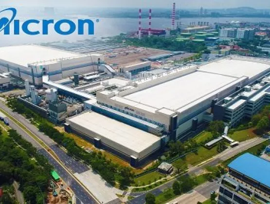
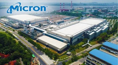
Making Strides TogetherKnowledge is power – especially when it is shared. This principle formed the foundation for Micron’s Go and See virtual visit of its Singapore manufacturing plant on 26 August 2020 as 27 companies including GLOBALFOUNDRIES, ST Microelectronics, Infineon, TEL, ViTrox , IBM, HP and UTAC joined the first-of-a-kind virtual factory visit. The chip industry powerhouses gathered to see how Micron’s Lighthouse frontend wafer fabrication facility leverages Fourth Industrial Revolution technologies to drive new production and cost efficiencies.They saw clear markers of a transformed organisation and spoke with working-level staff, managers and front-line employees. Company representatives also met virtually with Micron management teams from organisations that led its digital transformation – from pilot programs to integration at scale – to realise significant financial and operational benefits. The mix of technologies they deployed to make it all happen included artificial intelligence (AI), big data analytics and the Industrial Internet-of-Things (IIoT).Micron’s Singapore-based fab facility earned Lighthouse certification earlier this year from the World Economic Forum’s Global Lighthouse Network. The Go and See tour was co-sponsored by SEMI Southeast Asia and McKinsey Company.Transformation is CrucialBy embracing Lighthouse principles, semiconductor sectors and companies can accelerate their digital transformation to boost operational and financial efficiency while helping increase productivity across the electronics supply chain. It will take time for Southeast Asia semiconductor manufacturers to transform to digital operations, though we’re seeing growing interest in Industry 4.0 practices as they begin to understand that the deployment of new technologies and applications will help them better understand real-world benefits of smart manufacturing use cases and solutions. SEMI believes shining the spotlight on companies like Micron can illuminate the way forward for other companies to help drive the industry’s digital transformation. We look forward to seeing companies build on this momentum as they start to leverage leading-edge technologies to improve efficiencies and promote sustainability.Bee Bee Ng is president of SEMI Southeast Asia.
Read More
No, that wasn’t a fancy chandelier on the periphery of ES Design West’s exhibit area, the co-located event at SEMICON West. It was IBM’s Q quantum computer, a striking bit of industrial design that looks like a chandelier from a stately ballroom.While it resembled an ornate lighting fixture, IBM Q does much more than illuminate a room. The Q contains 20-quantum bits (20 qubits), equivalent to 2**20 or two to the 20th power classic bits. Impressively, IBM is currently readying (or may already have) a 50-qubit computer.During ES Design West, IBM demonstrated the Q Experience quantum cloud services platform and Qiskit, an open source quantum software framework. IBM’s booth staff showed how Q can solve problems beyond the practical reach of even today’s conventional supercomputers. Examples include the Traveling Salesman Problem (TSP) of finding the shortest route to enable the salesman to visit every city once and return to the starting point. Other examples are chemistry, drug and medicine discovery, weather and climate modeling, and security and advanced cryptography.The demos did even more, highlighting just how far semiconductor design and manufacturing advances have come to make quantum computing architecture possible.We have Dr. Jeffrey Welser, vice president of IBM Research–Almaden, to thank for bringing Q to SEMICON West and ES Design. During his keynote, The Future of Computing: Bits + Neurons + Qbits, he noted that Quantum computing holds the potential to solve problems even the most powerful classical computers cannot and challenges our community to drive innovation from materials to devices to systems. Both he and the booth staffers made the point out that Q will not replace conventional computing but augment it to solve complex problems beyond computational limits and/or the storage capacity of conventional computers.Challenges of Quantum Computing are not insignificant, however, and start with coherence time or the time interval over which the qbit is in a quantum state. The 20-qbit Q shown at ES Design West has a coherence time of 90 microseconds. Noise and variance are other challenges. The IBM booth staff said that a typical program must be run at least 1,000 times. Results are filtered with the extremes removed to get the most consistent result.Fault tolerance is high on the list of challenges as well because a solution for fault tolerance in quantum computing has yet to be discovered. Users like us take fault tolerance for granted in modern classical computers, addressed in hardware and firmware. Programmers don’t need to be concerned about it because the computer takes care of it through error correction.Finally, Q and most other quantum computers require near 0 Kelvin temperatures to operate. The refrigeration systems are large, expensive and not easily portable. Research is ongoing to find materials, such as carbon nanospheres, that will allow quantum computing at room temperature.Most experts agree that we are years away from practical deployment of large quantum computer systems. IBM’s open system for users around the world to access a Q computer to run programs is helping drive the way forward.Robert (Bob) Smith is Executive Director of the ESD Alliance, a SEMI Strategic Association Partner. He is responsible for the management and operations of the ESD Alliance, an international association of companies providing goods and services throughout the semiconductor design ecosystem.
Read More
Would you buy your next hotdog in parts, from un-coordinated suppliers? For example: Get the bun from a baker, the sausage from a butcher, mustard and/or ketchup and veggies from the nearest supermarket? If yes, you may find the sausage being too small, the veggies too big for the bun, and, when you finally finished adding mustard/ketchup and start eating, you may “enjoy” a cold sausage on a soggy bun!This “hotdog example” is just a very simple way to highlight the advantages of a well-coordinated semiconductor supply chain. What may be a few dollars and cents wasted in this hotdog purchase, can become millions of dollars lost to delays and inefficiencies during the roll-out of a new electronic system.Complexity is Increasing the ChallengeThe very innovative semiconductor industry is continuing to develop more complete and complex building blocks for electronic system solutions, with the intent of making our customers’ lives easier. However, every new technology takes increasingly more time for technical and business interfaces to mature before all the semiconductor supply chain members can serve customers in a smooth, efficient and cost-effective manner. In particular, coordination between design and manufacturing has always turned out to be in the critical path.SEMI, the manufacturers’ trade organization, and the Electronic System Design (ESD) Alliance, representing electronic design automation (EDA) tools vendors, developers of intellectual property (IP = ready-made building blocks for ICs) and IC design service providers, both recognized these challenges. Late in 2018, these two industry organizations decided to jointly address this painful, costly and often a very frustrating, yet critical path and became Strategic Association Partners, The goal is to establish a well-coordinated semiconductor supply chain.To make the value propositions of this partnership highly visible and demonstrate the first joint accomplishments, SEMI’s well-known SEMICON West conference and, in its first year, ES Design West, will be conveniently co-located in San Francisco’s Moscone Center from July 9 to 11, 2019. The synchronized schedules and geographic proximity of these events not only outlines the multi-faceted interdependence of manufacturing and design but encourages and enables conference attendees to do, what previously would have been viewed as “forming cross-border relationships.” It’s a new word now — please join the path to success and expand your network!Navigating SEMICON West and ES Design WestJust in case you are not yet planning to come to San Francisco early July, please check the Agendas-at-a-Glance for SEMICON West and ES Design West, to see how broad and valuable these parallel conferences are for your business. In addition, every customer, partner and semiconductor industry supplier can, from July 9 –11, walk from one conference section to the other, arrange face-to-face meetings, in dedicated meeting rooms, with representatives from both camps and discuss, from the first project planning step to the final production ramp-up, the many topics that need to be coordinated across parts or the entire supply chain to minimize delays and/or cost over-runs.Who Will Lead the Discussions?Conference attendees can, in addition to meeting many important supply chain partners face-to-face, hear about the latest technologies and market trends from key executives in our industry. Featured speakers are: David Pellerin, Head of Global Business Development, Amazon Web Services Lisa Su, President, and CEO, AMD Gary Dickerson, President, and CEO, Applied Materials Laurent Le Faucheur, Principal Engineer, Digital Signal Processing and Machine Learning, Arm, Ltd. Renee St. Amant, Ph.D., Research Engineer in Emerging Technologies and US Innovator of the Year, ARM Dean Kamen, President DEKA Research Development, Founder First and First Global Jeffrey Welser, Ph.D., Vice President and Lab Director, IBM Research-Almaden Dean Drako, President and CEO, IC Manage, Inc. Oreste Donzella, Sr. VP Chief Marketing Officer, KLA Corporation Prakash Narain, President, and CEO, Real Intent, Inc. Aart de Geus, Chairman, and Co-CEO, Synopsys, Inc. Manish Pandy, Fellow, Synopsys, Inc. Nate Baxter, General Manager, Development and Production Group, TEL US Like in previous years, SEMICON West and ES Design West offer a range of special features, addressing Smart Manufacturing, Smart Transportation, Smart MedTech and Smart Workforce development in dedicated pavilions as well as an AI Design Forum. Also, the many exhibitors from both camps will give conference attendees convenient opportunities to get to know new supply chain partners and/or refresh long-term business relationships. Search for the exhibitors you want to meet early July here. Questions to Ask for a Well-Coordinated Semiconductor Supply ChainIf I may, I would like to ask my many friends in the manufacturing camp to spend some time in the ES Design West section and ask the exhibitors a few questions, like: What can you do to get me to profit faster? To reduce development and unit cost? To improve yield, product quality, and reliability? When can you visit my team to discuss how your company can contribute to our goals?Vice versa, I would like to encourage my friends in the design camp to spend time in the SEMICON West section and ask exhibitors what their companies offer. When talking to manufacturers of IC, passive components or circuit boards, assembly and test houses, please ask very specific questions like: How can we help you reduce iterations between you and your customers? How can we help to improve IC test programs? How can we increase the throughput of your manufacturing equipment? How can we apply machine learning (ML) and Artificial Intelligence (AI) to minimize equipment downtime, improve yields and/or shorten production ramp-up?I can assure you that you’ll not only win great friends “across the border” but will be very impressed by the expertise you’ll find in the other camp and the willingness for and benefits of cross-border cooperation.I look forward to meeting you at SEMICON West and ES Design West. Also, if your schedule allows, mark your calendars for the June 12 MEPTEC Luncheon at SEMI in Milpitas, June 18 for the GSA’s Silicon Summit in Santa Clara and June 25 to 27 for the IMAPS SiP Conference in Monterey, CA. Hope to see you at one or all of these important events!Article originally published in 3D InCites. Herb Reiter is president of eda 2 asic Consulting.
Read More