downloadGroupGroupnoun_press release_995423_000000 copyGroupnoun_Feed_96767_000000Group 19noun_pictures_1817522_000000Member company iconResource item iconStore item iconGroup 19Group 19noun_Photo_2085192_000000 Copynoun_presentation_2096081_000000Group 19Group Copy 7noun_webinar_692730_000000Path
Skip to main content
Default Banner Image

high-volume manufacturing

SEMI spoke with Eyal Shekel, senior vice president of Service Strategy and Excellence at Tokyo Electron Limited, about the impact of artificial intelligence (AI) on smart manufacturing and how other fab solutions for smarter process tools are advancing semiconductor manufacturing.Eyal shared his views ahead of his presentation at the SEMI Fab Management Forum, 17 February, as part of the SEMI Technology Unites Global Summit, 15-19 February 2021, an online event. Join us to meet experts from Tokyo Electron and other key industry influencers. Registration is open. SEMI: AI technology is considered a key enabler for smart manufacturing. What are the latest trends? Shekel: The advent of advanced nodes and extreme complex 3D semiconductor geometry has lengthened time to market and increased costs in areas ranging from equipment development and large-scale metrology usage to monitoring yield inhibitors.AI is becoming a critical tool in the area of material informatics to determine suitable materials and processing techniques in order to meet the needs of future devices. Together with new materials and processes, the development and implementation of virtual metrology will enable accurate and almost absolute real-time monitoring of our customers’ device wafers at each stage of the manufacturing process.SEMI: What are the benefits of data analysis in the process from R D and Ramp-Up to High-Volume Manufacturing? Shekel: The new research field of materials informatics enabled by AI provides tools to guide the highly efficient discovery and optimization of production processes. For example, TEL has developed methodologies for co-optimizing processes and materials for etch rates.To monitor and manage the yield of semiconductor fabrication processes, direct metrology measurements are important. However, it is difficult to monitor all production wafers due to the time and cost involved. With deep learning AI, it is now becoming possible to predict every wafer’s metrology measurements based on production equipment data and previously processed wafer metrology variables. This enables total quality management and run-to-run control, while simultaneously reducing production costs and cycle time.SEMI: Can you tell us more about TEL Service Advantage?Shekel: TEL Service Advantage is a TEL global support organization that allows customers to select a service plan that fits their needs. Through TEL Service Advantage, we can quickly respond to customer requests and technical advancements. TEL Service Advantage provides various plans to maximize equipment maintenance efficiency for customers and productivity from equipment manufactured by TEL. TEL Service Advantage plans can be combined to meet customer needs and achieve maximum results.A key enabling element of TEL Service Advantage is TELeMetrics™. TEL analyzes equipment data from various sensors using a remote connection and, based on that analysis, provides solutions to customer-specific problems around equipment throughput and predictive maintenance.SEMI: How is AI helping during the pandemic? Can you share a success story? Shekel: The pandemic forced severe travel restrictions worldwide, making it very difficult or even impossible in many cases to visit our customers, as it is still the case today. Standard communication devices like smartphones and email helped at the beginning when TEL intensified the remote support by our Total Support Centre (TSC).TEL continued to develop its Service Advantage program quickly, and started using additional advanced tools and methodologies such as the following: Deployed AR (Augmented Reality) to remotely assist our customer and TEL engineers Secured remote connections into TEL tools to investigate parameters and logs, or to change set-up Used remote training courses that connects trainers via video conferencing systems and training tools in the factories to skill up engineers located in a different parts of the world Used AR glasses for tool start-up and troubleshooting Expanded TEL database global technology with multi-tool on languages search capabilities A key project at a customer site in Europe offers an excellent success story. Using all the approaches above, we collaborated with the local team to put a tool into production with no major delays. This was highly appreciated by the customer and very important for us.SEMI: What do you predict for the future? Shekel: Global technology infrastructure continues to develop and expand rapidly. Elements like 5G networks, IoT and advanced sensing capabilities will lead to what we call General AI, which will be based on neuro-like infrastructure. The auto learning will spread across domains and rely on internal logic and reasoning to automate many tasks that are manual today. In our industry in particular, General AI will enable workers to focus more on data analytics and future advanced R D rather than ongoing operations.SEMI: How can technology unite us? What do you expect from your participation at SEMI Technology Unites Global Summit?Shekel: Technology united us in the last 150 years. The connectivity started with telegraph and telephone and was used to exchange information over wider distances. Nowadays, video conference capabilities, AR and improving communications technology makes it much easier to unite people who are geographically dispersed. This becomes obvious and valuable especially during this pandemic period. As a fact, we are able to continue to perform all our key activities – our tool support, training and customer relationships – even if we cannot be present in person.The SEMI Technology Unites Global Summit is a great chance to stay connected to people and customers that I would normally meet at the SEMICON exhibitions.It also offers the opportunity to network with many more people who I would not be able to meet otherwise. Moreover, I can watch speeches and presentations at any time! Normally I would miss some programs since exhibitions and events took place at the same time.Eyal Shekel, senior vice president of Service Strategy and Excellence at Tokyo Electron Europe Limited, is a 27-year semiconductor industry veteran. Upon his graduation as a Mechanical Engineer from the Technion (Israel leading technical institute), he joined Applied Materials. In 1997 he moved on to Tokyo Electron (TEL) in Europe, served as the Regional Service Manager of Israel and, soon after, was appointed the company’s General Manager. Since 2005 Eyal has been part of TEL Europe senior management. He oversaw the Service and Support Operations for TEL Europe as a senior vice president until 2019. In his current role, he co-leads TEL’s Global Service Committee in Japan.The SEMI SMART Manufacturing Initiative is a global effort to promote awareness of and interest in smart manufacturing with a focus on delivering industry-recognized best-in-class programs and services to enable members to maximize product quality and productivity while reducing costs. Activities are focused on building out core capabilities to enable smart manufacturing across the microelectronics supply chain. MADEin4 is a consortium of 47 partners from 10 countries connecting the full range of supply chain – from semiconductor equipment manufacturers and system-integrating metrology companies to RTOS and key applications such as the automotive industry. The MADEin4 Project develops next generation metrology tools, machine learning methods and applications in support of Industry 4.0 high-volume manufacturing in the semiconductor manufacturing industry. Serena Brischetto is senior manager of Marketing and Communications at SEMI Europe.
Read More
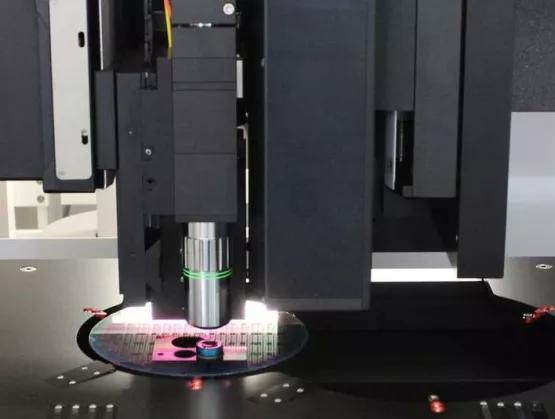
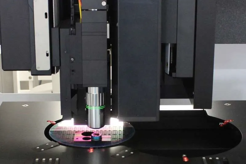
SEMI spoke with Thomas Fries, founder and CEO of FRT GmbH, about how hybrid metrology is shaping multi-sensor metrology tools to enhance measurement precision as the industry moves away from a single-sensor approach.Fries offered his views ahead of the SEMI MEMS Imaging Sensors Summit, 25 to 27 September 2019 in Grenoble, France. Join us at the event to meet experts from FRT Metrology and many other MEMS, imaging and sensors companies. Registration is open. SEMI: Metrology in front-end used to be straightforward. But then, as the number of tasks to be implemented increased, we moved to a multi-sensors approach. What drove this transition?Fries: I believe it´s more about software than about sensors. But of course the basis is the hardware. So, most metrology tools were designed around a specific sensor, e.g. a white light interferometer.A rigid frame, wafer fixtures, scanning tables etc. were then added to develop a complete system. In manufacturing more machinery was added, like handling systems, cleanroom equipment and more sensors, mainly for additive functions such as reading IDs or measuring temperature. The center was still the one and only sensor, being pimped more and more by some hardware features and a lot of software.SEMI: How are sensors and software shaping the way metrology is applied today?Fries: Today a huge number of optical sensors are available to provide various measurement options. But sometimes there are only very slight differences from one sensor to the other. A tiny variation may determine whether we solve a problem or end up fishing in troubled waters.And of course using different machines with those sensors requires high budgets for capital investment, used floor space, measuring time, etc. A multi-sensor platform solves all these problems. But again, it is the software that makes the real difference.SEMI: What lead to those advancements in metrology? What problems did they set out to solve?Fries: Metrology has been evolving ever since the measurement standards were established. The first challenge was to create a flexible mechanical platform that was also reliable and stable. All components were designed to be integrated into one system, mechanically, electrically and of course in the software.This level of integration requires not only an appropriate user interface, but also data formats and evaluation algorithms that leverage multi-sensor hardware. Today every metrology tool in the fab is justified by the application, not by specific sensors or specs. Of course the application leads to a set of specs, but the solution for the metrology task is realized within the software.New developments in metrology combine expertise in system design, physical knowledge in metrology and materials, mechanical engineering and also mathematical and software skills.The last step was the implementation of hybrid metrology functionality into a multi-sensor system that opens totally new doors in metrology. Before multi-sensors development, quite a few hitches could not be properly solved. SEMI: This is especially true when we consider applications in advanced packaging and MEMS manufacturing. What is in your opinion the main challenge?Fries: Specifically, in MEMS and advanced packaging we face multiple metrology challenges, as various processes run in one step and conditions on the wafer may vary quite often. In this case, a high degree of flexibility, up to the option to upgrade the metrology tool at any time or place, is a priceless advantage. Besides, cost effects for footprint, throughput and investment play a key role.A central task for nearly every customer application is to combine global measurements (complete wafer) and local measurements (per die) within one recipe. This is a perfect case for a multi-sensor platform. Measuring step heights and film thickness in one take is also an everyday routine. Combining those characteristics to measure hidden structures (hybrid metrology) is unique.SEMI: How will hybrid metrology enhance measurement precision and where do you expect the multi-sensor approach to be more applicable?Fries: The first advantage is the ability to measure properties that you cannot access directly. On top of that, all the previously mentioned features such as facing multiple metrology tasks, the combination of complete wafer and per die measurement are playing key roles. The precision of specific measuring tasks can be optimized by calibrating sensors against each other or combining results to get rid of noise or artefacts.MEMS and advanced packaging are natural playgrounds for hybrid metrology. But already today we see applications in high volume manufacturing in the 300mm fabs. As structures on wafers shrink, wafers are getting thinner and the whole process is becoming more and more complex. The classic one-sensor metrology tool is running out of gas. SEMI: What are your expectations regarding the summit in Grenoble, and for the future of the MEMS Sensors technology?Fries: FRT has always been very strong in MEMS and sensors and we have attended and exhibited at the SEMI MEMS Imaging Sensors Summit from the very beginning. The summit is always a very good meeting point for the community, and a perfect training session that gives participants extended updates in all fields. And of course, it grows our network and gives us the opportunity to show our latest products and applications.If you really want to know how the future of MEMS and sensors will look like, join the summit and don´t miss the chance to pass by the exhibition to meet FRT and many other industry leaders.Dr. Thomas Fries lives with his family close to Cologne. He is engaged in a variety of activities: as technical advisor to various ministries, supervisory board of PlanOptik AG, board and advisory board of IVAM, board member of COPT.NRW e. V., just to name a few. FRT supports many social projects as well as kindergartens and schools. Motorcycles and cars are still a great passion alongside his family.Serena Brischetto is senior marketing and communications manager at SEMI Europe.
Read More
SEMI met with Jay Zhang, business development director at Corning Incorporated, to discuss recent innovations at Corning that allow fine granularity CTE engineering as well as high Young’s modulus. We also talked about the impact of this work on in-process warp control, as well as the associated production methodology that provides rapid prototyping and high-volume manufacturing. We spoke ahead of his presentation at the 3D Systems Summit, 28-30 January, 2019, in Dresden, Germany. To register for the event, please click here.SEMI: What is Corning’s mission and vision and your role within the company?Zhang: Corning is one of the world’s leading innovators in materials science with a track record of 165+ years of life-changing innovations. We excel in glass science, ceramics science, and optical physics and succeed through sustained investment in RD E. Our products include Corning® Gorilla® glass, a durable material used on more than six billion mobile devices worldwide, and industry-leading LCD glass for display applications. We have recently dedicated a unit of the company called Precision Glass Solutions to address the emerging need for glass in the semiconductor industry. Here we apply Corning’s long history of glass science expertise and deep customer relationships in consumer electronics to support cutting-edge applications like wafer-level optics for precise 3D sensing and carrier solutions for temporary bonding applications in semiconductor manufacturing. It’s our most recent work in the Carrier Solutions product line that I’m excited to present: a new carrier glass product optimized for fan-out, called Corning Advanced Packaging Carriers.SEMI: What projects are you currently working on that you think will make a difference in 2019?Zhang: My team is excited to introduce Corning Advanced Packaging Carriers this year. This is a new line of product within our portfolio of Carrier Solutions. These ultra-flat glass carriers are specially developed to reduce customers’ challenge of in-process warp by up to 40 percent, which in turn helps advanced packaging customers achieve better yield.Corning Advanced Packaging Carriers feature high-stiffness properties and are available in a wide range of coefficients of thermal expansion (CTE) in fine granularity. These attributes help customers select an ideal glass carrier that will minimize in-process warp for their package. Furthermore, we make sample quantities of these carriers available in just four to six weeks to help maximize efficiency during customers’ R D process.My team is excited about the potential of this new product, but also encouraged by our results. We have already supplied this product and have heard from one of the largest semiconductor companies in Taiwan that it has reduced in-process warp by as much as 150μm.SEMI: Your presentation at the 3D Systems Summit will focus on Agile Manufacturing of Glass Carriers for Advanced Packaging. What exactly will you be sharing?Zhang: There is a lot of interest right now in using glass as a carrier substrate in temporary bonding applications in advanced semiconductor packaging – especially in fan-out processes. We also know that in-process warp is a significant challenge to companies pursuing advanced packaging because different CTE materials are added during the process. My team has done a lot of work to understand the impact that an ideal CTE glass carrier substrate can have on minimizing in-process warp. We have studied the available levers – both theoretical and in real-life fab environments – that can help address this challenge. I will present our findings on how it is possible to select a glass carrier with the ideal CTE and Young’s modulus to reduce in-process warp by up to 40 percent, and how Corning has developed an agile manufacturing platform to support customers with these ideal carriers from their R D stage through mass production.SEMI: What do you think will be a hot topic in the next few years?Zhang: We expect high-end fanout technology to address more applications beyond just mobile APs. There is also an interesting dynamic playing out between wafer-level and panel-level fan-out technologies. Corning is active in both areas. In developing and offering high performance glass carriers, we hope to help enable our customers to expand the fan-out applications space.SEMI: What are your expectations regarding the summit in Dresden, and why do you recommend your members and other industry leaders to attend the 2019 3D Systems Summit?Zhang: Europe is where some of the most advanced packaging technologies are born. Fan-out also saw early commercialization there. I hope to meet many scientists and technologists at 3D Systems Summit and exchange technical and business ideas. We also hope to get early feedback from other attendees about the value of our new product offering. Serena Brischetto is a marketing and communications manager at SEMI Europe.

Read More