downloadGroupGroupnoun_press release_995423_000000 copyGroupnoun_Feed_96767_000000Group 19noun_pictures_1817522_000000Member company iconResource item iconStore item iconGroup 19Group 19noun_Photo_2085192_000000 Copynoun_presentation_2096081_000000Group 19Group Copy 7noun_webinar_692730_000000Path
Skip to main content
Default Banner Image

electronics industry

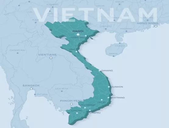
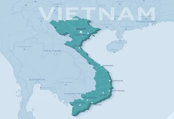
If you look at your clothes or shoes, there is a growing chance you will see the words Made in Vietnam printed on the tag. Since the United States lifted its trade embargo against Vietnam in 1994, the country has become the second largest exporter of apparel and shoes to the U.S. What may be less evident is the source of that new electronic gadget you received for Christmas, with its numerous parts, chips, and intricate supply chain. While light manufacturing has dominated Vietnam’s economic growth since the Đổi Mới economic reforms implemented in the 1980s, over the last decade the country has been repositioning itself to become a dominant player in the global microelectronics industry, a trend that has gained momentum in the wake of the U.S.-China trade war. In 2019, Vietnam ranked as the fourth largest exporter of electrical goods and components to the U.S. With exports doubling over the last four years and now exceeding $19 billion, surpassing Taiwan, Japan, and Korea (based on goods exported under chapter 85 of the Harmonized Tariff Schedule). Vietnam’s global electronics industry now accounts for about 40% of its exports, and the country seems to be just getting started. Early Entrants Though Vietnam owes its growing success in attracting foreign direct investment (FDI) in the semiconductor and microelectronics industries to the advent of China plus one – the business strategy to diversify business investments geographically – it was the few early entrants that gambled on this emerging market a decade ago that put Vietnam on the global stage. Of these early players, no other firm comes close to having the impact that Samsung has. It’s initial $670 million mobile phone manufacturing plant in the northern province of Bac Ninh in 2008 grew to a country-wide investment of $17.3 billion within a decade. Samsung is now Vietnam’s largest FDI contributor and accounts for more than 25 percent of its exports. Because of Samsung, Vietnam has become the second largest exporter of smartphones in the world. Around the same time, Intel opened its $1 billion semiconductor assembly and testing facility in Ho Chi Minh City, putting Vietnam firmly on the global technology map. More investors, like LG, Panasonic and Foxconn soon followed. Within a few years of these initial investments the industry was taking notice, illustrated by SEMI’s role in co-organizing the Vietnam Semiconductor Strategy Summits in 2013 and 2014. With SEMI SEA’s increased efforts to promote Vietnam as an important ecosystem in the electronics supply chain, more will be done to positively influence the growth and prosperity of its member companies in Vietnam. These early investors found Vietnam attractive for several reasons. Key among these are the country’s low wage rates combined with its favorable demographic structure – what the UN refers to as the golden population structure, which provides “Vietnam with a unique socio-economic development opportunity.” Companies are also attracted to the growing number of Free Trade Agreements (FTAs) that Vietnam belongs to, including the ASEAN Free Trade Area, CPTPP, the EU-Vietnam FTA, and, most recently, RCEP. Though the U.S. has yet to ink a trade agreement, the Singapore AmCham’s annual regional survey has consistently identified Vietnam as the most attractive country in ASEAN for a potential bilateral FTA partner with the U.S. Leveraging the Trade War If the plus one strategy was the catalyst that started this wave of electronics manufacturing in Vietnam, then the U.S.-China trade war was the enzyme that supercharged it. A common quip in Southeast Asia is that the U.S.-China trade war is over and Vietnam is the winner, and this is apparent in both trade and investment trends. According to the Asia Development Bank (ADB), the riff between the U.S. and China has caused a redirection in trade, as U.S. imports from the PRC fell by 12% in the first six months of 2019 while U.S. imports from Vietnam increased by 33%, with electronics and machinery accounting for the bulk of this jump. The ADB further reported that in a prolonged and intensified trade conflict, the worse-case scenario would result in Vietnam, Malaysia, and Thailand being the biggest winners, “in that order.” On the investment side, a March 2020 Gartner, Inc. survey of global supply chain leaders revealed that 33% had “moved sourcing and manufacturing activities out of China or plan to do so in the next two to three years.” While this survey did not mention specific winners, the ADB reported that “newly registered FDI in Vietnam from the PRC and Hong Kong rose by 200% year on year in the first seven months of 2019,” indicating the move of Chinese suppliers to Vietnam. Additionally, a review of recent press reports indicate firms like Apple, Nintendo and Dell are encouraging suppliers to move parts of their supply chains to Vietnam. These suppliers are complying, with Compal Electronics, GoerTek, HZO, Inventec, Luxshare Precision Industry, Pegatron, USI and Wistron all reportedly announcing plans for new investments in Vietnam. Manufacturing Hubs Within Vietnam, microelectronic facilities have concentrated in a few geographic hubs. In the south, the Saigon High Tech Park in Ho Chi Minh City attracted early entrants Intel and Samsung, with firms like Nidec and Jabil soon following. The largest investment capital, however, developed in the northern provinces that ring Hanoi. Bắc Ninh, an hour’s drive from Hanoi, was the site of Samsung’s first investment and has since attracted Foxconn and Canon. More recently, firms have been drawn to the port city of Hải Phòng, the country’s third largest city, which is already home to Samsung and LG. The city’s close proximity to other manufacturing clusters, its new deep-water port, and its expressway that provides a 12-hour trucking route to China’s electronics epicenter in Shenzhen are helping make the city Vietnam’s new high-tech production center. In 2019, LG Electronics moved its entire smartphone production line from South Korea to Hải Phòng, and in 2020 Pegatron reportedly chose the city for its $1 billion investment plan. Local phone manufacturer VinSmart is also producing the country’s first 5G smartphones in Hải Phòng. In November, USI, a subsidiary of Taiwan-based ASE Holding, broke ground on its first production base in Southeast Asia, a $200 million phase-one investment in the production and assembly of chips for wearable electronic devices. USI’s investment, which is moving into the internationally managed DEEP C Industrial Zones in Hải Phòng, is “intended to move us closer to our overseas customers and accommodate their ever-increasing demand,” according to Mr. Kuei Chun Chi, the firm’s Manufacturing Service Director. “North Vietnam, with its strategic geographical position and an extended infrastructure in place, offers USI an optimal way to facilitate fast and flexible response to customers' orders.” Though the Covid-19 pandemic has dampened the pace of new investments in Vietnam’s microelectronics industry, it has also amplified the country’s attractiveness to investors. Vietnam was successful in containing the outbreak through aggressive quarantine and contact tracing measures, and as a result its economy has the brightest outlook in the region. The ADB forecasts the country will be one of the fastest-growing economies in SEA in 2021, with GDP estimated at 6.8%. The Ministry of Industry and Trade is also reporting that several of the world's largest technology corporations plan to shift their production chains to Vietnam post-Covid-19, an indication that technology firms will accelerate relocation plans in 2021. Vietnam’s successful response to the pandemic, combined with its strategic location, low wage rates and foreign trade agreements, will ensure that the region continues to benefit from the shift in supply chains in Asia, making it the new destination for electronics manufacturing. About the Author Stuart Schaag is Principal at E-Ward Trade Consulting LLC, which assists firms that are expanding their presence in the global marketplace by creating strategies combining market analysis, business development, commercial diplomacy, and relationship building. He previously spent 25 years in various domestic and overseas positions in the U.S. Department of Commerce’s International Trade Administration. Stuart served as the Commercial Counselor at the U.S. Embassy in Hanoi from 2014-2018 and resided in Vietnam until 2020.
Read More
A lot has happened in fifty years, particularly when it comes to the microelectronics industry. Founded in 1970 by a group of semiconductor industry pioneers who believed that co-opetition — instead of traditional competition—would produce a more vibrant emerging industry, SEMI was born as an industry association.It's fitting during this week’s 50th annual SEMICON West (July 20-23, 2020) — a virtual event for the first time — that SEMI Chief of Staff Bettina Weiss offers her perspectives on the evolution of SEMI from one of the best seats in the house: the 24 years that she has spent helping the association change and grow.Vetrano: You’ve enjoyed a long rich history with SEMI, and now serve as the association’s first chief of staff. What roles have you played at SEMI up to this point?Weiss: I cut my teeth at SEMI by joining SEMI Standards, first serving as standards coordinator at SEMI Europe from ’96-’97. Over the next 11 years, I held a variety of positions at SEMI Standards, culminating with director of international standards from 2003-2008. Given that experience, I have to admit that SEMI Standards are still near and dear to my heart.I moved on to several leadership positions in our former global photovoltaics/solar business through 2014, and toward the end of that stint, I assumed additional responsibilities, becoming vice president of business development. That’s where I dove headfirst into expanding SEMI into emerging regions, including Vietnam, India and Latin America. SEMI goes where members see (or want to better understand) new opportunities, especially in places that had ambitious plans for fabs for microelectronics, including semiconductors and MEMS.In 2018, I became SEMI chief of staff, reporting directly to our president and CEO Ajit Manocha.Vetrano: Now I hardly know where to start! Since I have to decide, what does it mean to be SEMI chief of staff?Weiss: As the first chief of staff, I’ve been able to shape the position, combining the support of critical efforts driven by Ajit with additional project management responsibilities like our Smart Mobility initiative.Working with experienced leaders in our industry, such as the Board of Industry Leaders (BIL), is one of the more rewarding parts of my role at SEMI. The BIL is a group of global executives tasked with advising SEMI on strategic planning, especially when it comes to future-looking initiatives like Smart Mobility, Smart MedTech, Smart Manufacturing, and Smart Data/AI.A lot of the other things I do are meant to support the whole SEMI organization, in partnership with other senior leaders such as Michael Ciesinski, vice president of technology communities, as we create business plans and examine new revenue models that will keep SEMI sustainable and viable for the future. This includes issues as varied as workforce development and diversity and inclusion, and the new digital platforms we use to engage with our members.Vetrano: How does SEMI Smart Mobility initiative exemplify the model of engaging end customers in vertical markets that are important to members?Weiss: When you look at the rapidly increasing number of chips and sensors in and around vehicles, Smart Mobility at its core brings together both the semiconductor/sensor and automotive/mobility supply chains for a more transparent dialogue about needs and wants along the entire supply chain. We are thrilled to count automotive OEMs Volkswagen and Audi as SEMI members. We also work with Tier 1 suppliers such as Continental and many others to promote the open exchange of ideas and foster collaboration among all stakeholders.Smart Mobility is a good example of how SEMI connects two worlds that are now interdependent for the mutual benefit of all players. Automotive companies and component suppliers want to better understand new technology capabilities that enable tomorrow’s infotainment, safety, security and communication protocols. And semiconductor, sensor and component companies see huge upside in supplying the equipment, materials, devices and subsystems that enable the future of mobility. Smart Mobility is a win-win, and the founding concept of our Global Automotive Advisory Council (GAAC).Vetrano: As we look to COVID-19, the single most important event to influence the microelectronics industry — and every other industry — why is SEMI membership more important now than ever?Weiss: Our industry is facing a triple whammy of challenges: a global pandemic, ongoing global trade tensions that impact interdependent supply chains, and a global economic crisis. All these challenges will require our members’ ingenuity, innovation and collective action to overcome them. But inherent in those challenges are tremendous opportunities, and I have no doubt that our members and the entire global electronics ecosystems will find ways to help everyone prosper and advance.COVID-19 has had a huge impact on our members. From the onset of the pandemic, we’ve provided our members with resources including best business practices, insights and data from industry experts to help them respond to a virus that has already changed so many things we took for granted before March. Additionally, SEMI has also advocated with governments around the world on behalf of the industry for essential business status and essential travel to sustain operations. Visit SEMI COVID-19 Resource page for information on industry best practices and much more.Vetrano: Before we look forward, what has changed dramatically in microelectronics since you started at SEMI?Weiss: Through my work with SEMI, I’ve witnessed dynamic, dramatic and sustained change in the microelectronics supply chain. Into the late 1990s, SEMI represented primarily semiconductor equipment and materials suppliers, and we worked with chipmakers – our members’ customers. That’s where a lot of important Standards work happened, for example, and the supplier-device maker relationship was pretty much our world. Over the years, we saw significant change in how companies partner and do business with one another. The digital transformation we’ve been witnessing for the past few years was the impetus for expanding our reach to bring companies in the extended electronics manufacturing and design supply chain together, from sand to system, so to speak. That was also when we invited associations representing flexible hybrid and printed electronics (FlexTech), MEMS and sensors (MSIG), and electronic system design (ESD Alliance) companies to join SEMI and our other technology communities for maximum cross-pollination. That’s because everything needs microelectronic devices and systems. Vetrano: Looking ahead now, what is can the microelectronics industry do to benefit humanity?Weiss: Semiconductors and sensors are often the unsung heroes of progress. Microelectronics can help bring prosperity to the billions of people now struggling on our planet. It can improve access to education for people through e-learning, it can advance agricultural production and streamline the food supply chain to help feed the world’s hungry, it can monitor the quality of the water we drink and the air we breathe, and it can get you in front of a doctor even in the most remote village in India.The beauty of microelectronics is that we are not gated by innovation. As the brilliant visionary Arthur C. Clarke once said, “The only way of discovering the limits of the possible is to venture a little way past them into the impossible.”As an industry association that helps technologists to venture beyond “the limits of the possible,” I invite like-minded technology adventurers to engage with SEMI, starting with registration to this week’s SEMICON West – our first virtual show.As chief of staff, Bettina Weiss reports to SEMI President and CEO Ajit Manocha and manages a broad portfolio of responsibilities. Major focus areas include advancing specific global strategic initiatives such as thought leadership (Think Tanks) and SEMI Smart Transportation vertical application platform, improving organizational efficiency, alignment and financial sustainability, acting as senior liaison to SEMI Board of Industry Leaders, leading strategic partnerships and M A activity, and supporting Manocha in creating a highly effective, agile global association.Maria Vetrano is a PR consultant at SEMI.
Read More
Sapphire is a precious gemstone, consisting of aluminum oxide (α-Al2O3) with occasional traces of other elements such as iron, titanium, chromium, vanadium or magnesium. While sapphire stones found in nature mostly go to jewelry applications, the lab-grown sapphire – produced in a scale of up to several hundred tons per year – is widely used by the electronic industry. Now one can hardly find a branch of technology where this crystal is not used.Sapphires are mainly applied in infrared optical components, high-durability windows, wristwatch crystals, and the very thin electronic wafers used as the insulating substrates of solid-state electronics. High thermal conductivity, low reactivity, and appropriate unit cell size make sapphire an ideal material for a wide range of such electronic substrates for manufacturing of components such as LEDs and CMOS chips.SEMI spoke with Ivan Orlov, CEO of Scientific Visual, after his presentation at SEMI Strategic Materials Conference at SEMICON Europa, 12-15 November, 2019 in Munich, Germany, to learn more about the future of sapphire.SEMI: Why is sapphire an ideal material for a wide range of electronic substrates? Orlov: Sapphire undoubted advantages are its chemical inertness and ability to withstand high temperature, radiation and mechanical loads. In addition, it exhibits low dielectric loss and very good electrical insulation that makes sapphire a good candidate for substrates for LEDs and laser diodes or wafers for epitaxial growth. However, the most important advantage is that sapphire crystal lattice does very well matching semiconductor materials deposited to its surface, in particular nitrides of group III elements. To plainly benefit from these features, the grown sapphire must have as few macro- and micro-defects as possible, as substrate defects are inherited by semiconductors layers grown on the substrate surface. Hence the importance to detect defects in the raw sapphire material. This is the area where our team at Scientific Visual contributes. SEMI: Flaws are usually identified only after costly wafering and polishing steps, because rough surface of raw crystals prevents detection of the defects. What can be done to prevent defects?Orlov: Today, major players are investing in growing larger crystals without mastering in depth the growth process. Let’s face it, the semiconductor substrate industry, which is primarily based in Asia, is using empirical research methods. The raw sapphire boules are still inspected manually, and this qualitative assessment is exploited in two folds. The first step is to further process the boule. Furnace operators then adjust the growing parameters depending on the results of the manual inspection.Due to the lack of visibility into internal crystal defects, the crystal growth and its downstream processing remain an art rather than a science. The primary reasons are the difficulty to measure, locate and quantify precisely the defects in the full crystal volume. Scientific Visual equipment enables defects in raw boules to be fully quantified and categorized. With such objective measurements and knowing the full set of growth parameters, the Process Engineering (PE) team can, with the assistance of deep learning algorithms, considerably improve the growing process. Our quality control tools give Process Engineering team the “eyes” to see complete defect distribution in raw crystals, enabling it to make minor modifications in the growth process to improve yields, reduce costs and shorten the time to market for products.SEMI: What lead to those advancements and what problems did your team set out to solve? Orlov: Breakthroughs in immersion tomography, machine vision and parallel computing drove advancements in automated quality control technology. Previously crystal inspection accuracy was limited by the acuity of the operator’s eye and subjective bias. Light distortion and the diffusion of crystals made it impossible to accurately identify internal defects.Scientific Visual equipment give operators an undistorted 3D view of all defects in a crystal boule or ingot. However, only deep learning technology can correlate a hundred thousand growth data points to identify a final defect pattern.Defect pattern in non-processed item cored from EFG sapphire plate. Well visible is a typical wavy pattern of surface layers and sandwich structure in the volume. Color code marks sapphire defect density: from deep blue (non-defective material) to deep red (highest defectiveness.) SEMI: What challenges are addressed by your approach? Orlov: Increasing the yield of semiconductor substrates like Sapphire, Gallium Nitride and Silicon Carbide is paramount to reducing the price of wafers while increasing their quality. The upstream growth and downstream wafering processes are not deterministic. So far, most of the producers can only determine the quality during the late stages of the process. This condition creates huge constraints for teams in charge of production and processing. Automated Quality Control (QC) at the early stage of the production chain relieves all the unknowns, ultimately reduce the cost of material.SEMI: And what are the main opportunities?Orlov: There are massive opportunities to increase the yield and to ease the full processing chain from growth to the wafering process. Objective Quality Control (OQC) paves the way to industry-wide standards that categorize crystal quality at each step of growth to enable full certification of the defectiveness of the material and facilitate its trade and exchange.SEMI: What’s one of your predictions for the future of new materials?Orlov: The explosion of e-mobility and electric vehicles and the development of other green technologies will drive rising demand for low-defect sapphire, silicon carbide and gallium nitride substrates thanks to the streamlining of the full processing chain. Manual quality control will soon give way to full automation as quality control in sapphire and other raw crystals production is the only missing link in a fully automated semiconductor production chain. I believe that in five years, automated raw crystal inspection will become standard in the industry. Our mission is to empower every crystal grower to achieve this important milestone.Dr. Ivan Orlov obtained a Ph.D. in Crystallography from the Federal University of Technology in Switzerland EPFL and an MSc in Solid-State Physics in Moscow, Russia. Ivan co-founded Scientific Visual in 2010 to answer the challenge of the synthetic crystals industry struggling with high defect yield. Prior to this he worked in a company specialized in diamond optics. He has more than 10 years of experience in R D with focus on optical materials, industrial crystals and non-destructive quality control technologies. Dr. Orlov was a SEMI Task Force member for sapphire standard development in China and collaborates with ISO committee in Switzerland to establish industry-wide sapphire quality standards.Serena Brischetto is senior marketing and communications manager at SEMI Europe.
Read More
With one of the oldest and largest public education systems in the developed world, how well does the US public education system serve the global electronics industry? Public education in the US has had time on its side. In 1635 the Boston Latin School became the first public school in the US. Boston Latin was originally a boys-only secondary school that taught Greek, Latin and the humanities. It wasn’t until 1918, however, that the US government required all children to obtain at least an elementary-school education – available to them through free public schools. As public education increasingly served the masses rather than just the elite, a balance of humanities, mathematics and science began to replace the classics.While free public education in the US got a comparatively early start, most American students score lower in science and math than students in many other developed nations. According to a 2017 Pew Research Study, 15-year-old American students ranked 24th in the world in international standardized age-group science testing and 38th in the world in standardized mathematics testing. While test scores are just one measure of proficiency, do they in some way reflect a lack of motivation to study science and math because of students’ unfamiliarity with STEM careers? Source: Pew Research. See article. Make STEM RelevantIf we want the US to remain a leader in the global electronics industry, we need to pay attention to the disconnects between academics and workforce development. We must help show students at an early age that STEM careers can be exciting, creative and fulfilling, and that math and science are essential to STEM.Ways to Get InvolvedWhether you work for a large publicly traded electronics manufacturer, an equipment or materials supplier, a foundry or a startup, you can take action to support student engagement in STEM. Here are a few ways to get involved:Participate in Community Programs One fun way to inspire budding technologists is to sponsor one of the FIRST programs for students. These age-segmented competitive programs range from FIRST LEGO League, Jr. Challenge for six-ten year-olds to FIRST Robotics Challenges for high school and college students, giving you the opportunity to sponsor a team or even to coach.Our company sponsors Team TNT, a Southern Oregon-based team that placed among the world’s top high school robotics teams at the spring 2018 world championships. We also brought two members of Team TNT to SEMICON West 2018, where they attended SEMI’s three-day High Tech U and presented their insights on building their FIRST Challenge robot at the Smart Workforce Pavilion. Margaux Quady (L) and Matthew Mills (R), Team TNT members, presented at SEMI’s Smart Workforce Pavilion at SEMICON West (Rogue Valley Microdevices) Concerned about the dearth of girls interested in STEM — and the small numbers of women in engineering careers? Look for your local equivalent of the Advocates for Women in Science, Engineering, and Math (AWSEM) Symposium, a day-long program for middle school girls. One of our engineers, Jennifer Devin, gave a hands-on workshop on deconstructing smartphones to showcase the silicon chips inside them. If you cannot find something like AWSEM, check out national programs such as the Society for Women Engineers (SWE)’s SWENext program for girls ages 13-18 as well as Girl Powered.Partner with Local SchoolsYou would be surprised at the opportunities to present what you do in the classrooms of school-age children. Take after Allyson Hartzell, managing engineer at Veryst Engineering in Needham, MA. Allyson speaks with students in her local elementary schools of Somerville and Cambridge, Massachusetts because she thinks that we must reach younger children to get them excited about STEM learning. “Waiting until middle school or high school to help students visualize the real-world appeal of STEM careers is just too late,” said Hartzell. “I’ve had amazing experiences working with local elementary-school students. Students become engaged when you show them real-world examples such as electron micrographs of MEMS.”Many middle schools and high schools also look to their communities to provide tutors in STEM subjects. Check with the community liaison at your local school to get started.Engage in Internship ProgramsInvolvement doesn’t stop in the K-12 grades. Seek out a local university’s internship program and hire some interns in that program to work at your company. The interns will gain valuable applied experience in your environment, and you might find young engineers who would love to join your company after they graduate. Oregon’s MECOP, an engineering-specific internship program founded on close industry-university collaboration, has been amazing for our recruitment. Some of our finest engineers were once in the MECOP program, including our engineering manager.Anything you do to get involved in inspiring coming generations of students to explore STEM — no matter how small your action — will make a positive difference in helping US students become better prepared to enter a technology-focused workforce. Through collaboration and creativity, we can help US companies keep the global electronics industry moving toward greater innovation. Jessica Gomez, CEO and co-founder of Rogue Valley Microdevices, entered the semiconductor manufacturing field in 1998 at Standard Microsystems Corporation of Hauppauge, New York where she acquired valuable knowledge in both semiconductor processing and production management. Jessica also held positions at Integrated Micromachines and Xponent Photonics prior to co-founding Rogue Valley Microdevices in 2003. As head of a technology company, Jessica recognizes the criticality of workforce development – and has become an advocate of STEM education. Rogue Valley Microdevices supports STEM initiatives for middle-school girls, a competitive robotics team for high school students, and a college internship program specifically for engineers.Expanding her energies beyond the company she co-founded, Jessica is also applying her passion for change to politics. She is currently campaigning for the Oregon State Senate.For more information, visit Rogue Valley Microdevices.
Read More