downloadGroupGroupnoun_press release_995423_000000 copyGroupnoun_Feed_96767_000000Group 19noun_pictures_1817522_000000Member company iconResource item iconStore item iconGroup 19Group 19noun_Photo_2085192_000000 Copynoun_presentation_2096081_000000Group 19Group Copy 7noun_webinar_692730_000000Path
Skip to main content
Default Banner Image

chip design

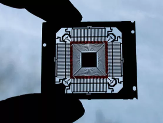
The semiconductor industry is undergoing a rapid transformation. Artificial intelligence (AI) applications, such as agentic and physical AI, push compute demands to unprecedented heights, prompting the semiconductor industry to push the boundaries of 2nm technology and beyond. Yet, as we move to these advanced semiconductor technology nodes, it has become increasingly challenging for academic research to remain closely connected with the fast-evolving industrial developments, limiting academic researchers in driving innovation. Europe’s NanoIC pilot line, a pioneering European initiative, hosted by imec, is addressing this challenge by offering pathfinding process design kits (P-PDKs). To cover the potential of these P-PDKs and their impact on Europe’s semiconductor ecosystem, we sat together with Professor Mehdi Tahoori (professor at Karlsruhe Institute of Technology) and Anita Farokhnejad (DTCO Program Manager at imec).SEMI: What exactly is a P-PDK, and how does it differ from traditional PDKs?Farokhnejad: At its core, a process design kit (PDK) is a software environment that enables circuit designers to simulate, validate, and optimize chip designs using realistic models of chip technology. Consider it a blueprint or a simulation toolkit allowing chip designers to explore performance, power, and manufacturability of a new chip architecture in a virtual sandbox. What sets P-PDKs apart is that they anticipate future technologies. Unlike traditional PDKs, which are based on existing technologies, P-PDKs are built on predictive models of future nodes and architectures. This allows researchers to explore system-level trade-offs, assess architectural implications, and prepare design flows before a technology reaches maturity. SEMI: Why are they so crucial for academia?Tahoori: For decades, academic researchers could contribute to semiconductor innovation using abstraction layers that allowed them to design and test new architectures without direct access to the latest technologies. This approach worked well until the industry reached the 20-nanometer node. At that point, the complexity of semiconductor design increased, with the introduction of advanced device architectures like FinFETs, nanosheets, Forksheets, CFETs, and novel integration solutions such as 3D stacking and chiplet integration.Transistor scaling in the AI eraTraditional abstraction models could no longer keep up with these advances, and the gap between academic research and industrial practice began to widen. This growing gap started to limit academia’s ability to participate in semiconductor paradigm shifts, such as CMOS 2.0 and new computing architectures. P-PDKs, enabled by the NanoIC pilot line, aim to bridge this gap, restoring the connection between academic thinking and industrial progress.SEMI: How does this support semiconductor innovation in Europe?Tahoori: Universities are ideally positioned to drive out-of-the-box innovation and invent new paradigms for computing. This is where universities truly excel. But to do that, they need access to the latest technologies and tools. We see for example a strong focus on the AI revolution and how the microelectronics industry is enabling that transformation. To meet the demands of AI applications and the computing power they require, we need to design new computing architectures based on advanced technology nodes. This is precisely the academic area of expertise. To design these new AI computing architectures, however, we need the most advanced technologies available. The P-PDKs for advanced nodes provided by the NanoIC pilot line now make this kind of research possible at universities. Something that was not feasible before.Additionally, the P-PDKs also provide an important reference technology and platform to benchmark and validate these innovations within a next-generation design roadmap. This means researchers can test their novel architectures against realistic process and performance metrics.SEMI: Are they only available for academia?Farokhnejad: The NanoIC P-PDKs are meant to be accessible to foster innovation across Europe’s semiconductor ecosystem. These advanced PDKs are therefore also available to European research organizations, startups, and industry partners. Access is facilitated through Europractice, where eligible users can apply by signing a Design Kit License Agreement (DKLA). Once approved, they gain access to the PDKs.SEMI: What other technology nodes are NanoIC’s PDKs addressing?Farokhnejad: The first P-PDK was released in June (first version of the N2) and supports frontside and backside routing with TSVM, standard cell libraries, and multiple VT flavors for early-stage design exploration. Upcoming releases include new versions of the N2 P-PDK, as well as A14 and A7 PDKs, eDRAM and SOT memory PDKs, and advanced interconnect solutions such as redistribution layers (RDL), hybrid bonding, and interposers.Those interested in learning more about the NanoIC ecosystem and the research enabled by the P-PDKs can meet representatives and partners of the NanoIC pilot line during SEMICON Europa, November 18-21 at booth C2417 in Messe Munchen. More information about the initiative is also available on the NanoIC website.BiosMehdi Tahoori, Professor Chair of Dependable Nano-Computing - Karlsruhe Institute of Technology Mehdi B. Tahoori is Professor and Chair of Dependable Nano-Computing at the Karlsruhe Institute of Technology (KIT), Germany, and guest professor at imec, focusing on CMOS 2.0 and future chip technologies. He previously worked at Xilinx (USA), Fujitsu Labs (USA), and served as a junior professor at Boston Northeastern University (USA) and as a visiting professor at the University of Tokyo (Japan). He earned his B.S. from Sharif University (Iran) and M.S./Ph.D. from Stanford (USA). Prof. Tahoori is Deputy Editor-in-Chief of IEEE Design and Test Magazine, is a former Editor-in-Chief of Elsevier Microelectronic Reliability and has chaired major IEEE symposia. His honors include multiple best paper nominations and conference awards, the US National Science Foundation Early Faculty Development (CAREER) Award (2008), an ERC Advanced Grant (2022), and an IEEE fellowship.Anita Farokhnejad, DTCO Program Manager - imec Anita Farokhnejad earned her PhD from Universitat Rovira i Virgili (Spain), specializing in FEOL and device modelling. She joined imec in 2021 as an R D Engineer, focusing on BEOL optimization and future roadmap development. Collaborating closely with integration and physical design teams, she develops models for PnR data analysis and BEOL optimization. Her recent work on the enhanced Ring Oscillator (eRO) model aids in the early assessment of new materials and BEOL boosters. In August 2023, she advanced to team lead for PDK Enablement, translating advanced semiconductor nodes into Pathfinding-PDKs. Farokhnejad is also dedicated to education, conducting courses that make sophisticated technological concepts accessible to both industry veterans and aspiring engineers. Currently, she serves as Program Manager of DTCO at imec, where her contributions continue to drive innovation in the semiconductor industry.AcknowledgementThis work was enabled by the NanoIC pilot line. The acquisition and operation are jointly funded by the Chips Joint Undertaking, through the European Union’s Digital Europe (101183266) and Horizon Europe programs (101183277), as well as by the participating states Belgium (Flanders), France, Germany, Finland, Ireland and Romania. For more information, visit https://www.nanoic-project.eu.DisclaimerFunded by the European Union. Views and opinions expressed are however those of the author(s) only and do not necessarily reflect those of the European Union or Chips Joint Undertaking. Neither the European Union nor the granting authority can be held responsible for them. SEMI ContactJames Lam, Business Development ManagerEmail: [email protected]
Read More
In the early 1990s, engineers of varying degrees of skill with a powerful PC set up shop designing and selling blocks or libraries of reusable components with a defined interface and behavior. These blocks, known as intellectual property, or IP, were then (and still are) integrated into a larger design. While the new market segment created excitement and new opportunities, it also was untested and created uncertainty. Many fledgling companies failed. It’s a different story today. Arm, as well as Cadence and Synopsys, are silicon IP suppliers and the segment’s yearly revenue tops $4 billion, a long way from those early garage startup days. ESD Alliance member CAST, a silicon IP provider since 1993, participated in the remarkable growth and impact on the semiconductor industry. Nikos Zervas, CAST’s CEO, and I discuss those early days of the IP business and what’s ahead. Smith: What were the early days of silicon IP like? Zervas: In those early Wild West days of IP, vendors and customers both wanted to benefit from IP, but nothing was standardized, and people just tried things to see if they worked. The perceived barrier to entry was low: hundreds of IP companies sprang up thinking they only needed RTL coding skills and tools, an FPGA to prototype, and a few thousand dollars to invest. IP deliverables, quality standards, and business practices varied from vendor to vendor and over time. Risk was high, and there are many horror stories of re-spins or market failures due to faulty IP cores. Smith: How has the silicon IP market changed from its early days? Zervas: Firms delivering high-quality IP and providing outstanding customer support survived. Others disappeared. Eventually the industry centered around a reasonably common sense of IP requirements and quality and a consistent set of business practices. IP product complexity has driven upwards as SoCs have grown. The largest ASICs used to approach a few million gates; today they’re hundreds of millions, and the granularity of IP has evolved from small functions to pre-integrated subsystems. Early on, a designer doing image processing might license individual functions like a Finite Impulse Response (FIR) filter or a Discrete Cosine Transfer (DCT) block. Today, instead they would license a complete JPEG compression core containing those functions and more, or even a complete black box subsystem streaming processed, stabilized, compressed video over Ethernet. IP selection criteria have also changed. Early IP was handcrafted to eliminate every extra gate, as being a few thousand gates smaller was a killer advantage in the era of 180nm ASIC processes. Today, at 7nm or 5nm process, tens of thousands gate differences are just noise, and it’s usually the reliability, functionality, and performance of an IP core that matter most. Smith: When did the silicon IP market start to take off? What was the driving force? Zervas: By the early to mid 2000s, uncertainty about what IP was and how best to use it – and the early wave of less-than-great providers – were being replaced by increasing acceptance and emerging best practices. The introduction of smartphones, the wild growth of Internet of Things applications, growing automotive system sophistication, and other advances fueled the explosion of the IP market in the late 2000s. In fact, according to the ESD Alliance Electronic Design Market Data Report, revenue from IP licensing today has surpassed the license revenue from front-end EDA tools. This would have been unimaginable in the late 1990s. Smith: How has silicon IP changed chip design? Zervas: Designers today must develop massive, complex systems with an even tighter time to market. Only the higher level of design abstraction and the distributed expertise that silicon IP provides make this possible. But IP also increases the challenge of differentiation: With the same IP available to everyone, how do you design a product that stands out in its market? The answer to differentiation today lies mainly in clever SoC architecture. Delivering better features with superior performance, lower power consumption, or other winning characteristics now depends not so much on perfecting each separate IP block but rather from selecting the best IP for the system’s requirements, integrating those IP cores for clean communication and efficient resource sharing, and other smart system-level decisions. It’s similar to modern building design: Every firm has access to the same materials and tools – concrete, glass, etc. – but only a few produce exceptional buildings. Smith: It seems that are several different business models for IP licensing, such as up-front license fees, subscriptions, royalties, or a combination of these. Do you think the IP market will gradually align around one basic model, or will it continue as is with a variety? Zervas: Different models serve different needs. For example, commodity IP like a SPI interface can’t demand royalties, but unique, leading-edge IP – like a 112Gbps SERDES – still can. I believe the market will continue with different business models, though the number of different models may shrink and their terms begin to align. About Nikos Zervas Dr. Nikos Zervas is the chief executive officer of CAST, Inc. He co-founded image and video compression IP developer Alma Technologies in 2001, and led the bootstrapped firm as chairman and CEO for nine years before joining CAST. He was a founding member of the Hellenic Semiconductor Industry Association and served on its board for several years with responsibility for strategic planning. He is a senior IEEE member and member of the Technical Chambers of Greece, had contributed to the GSIA's IP Working Group, and has published multiple technical papers on data compression design and related topics. Robert (Bob) Smith is executive director of the ESD Alliance, a SEMI Technology Community.
Read More
Alameda, Calif.-based Verific Design Automation, a member of the ESD Alliance, made its name in the electronic system design and semiconductor industry supporting companies ranging from startups to billion-dollar industry leaders such as Synopsys, Cadence, Siemens EDA, Xilinx, Microchip, NVidia, Infineon, Qualcomm, Renesas and Samsung. Its software is used as the front end to design automation tools such as synthesis, simulation, debug, and formal verification. I spoke with Verific president and COO Michiel Ligthart about homegrown and open-source EDA tools and other recent trends in chip design. Smith: What trends are you seeing in chip design? Ligthart: Semiconductor companies are starting to build a portfolio of intellectual property, including homegrown electronic design automation (EDA) tools, that they want to keep secure and differentiated from their competitors. The increased interest in internally developed and supported EDA tools is a trend we started to see about two years ago. It’s not simulation, synthesis or place and route (P R). Instead, it’s pieces of a chip design flow optimized for a company’s specific needs. In the past, a semiconductor company would either standardize on one EDA company’s chip design flow or mix and match best-in-class tools from different vendors. The common denominator was that they used off-the-shelf products. If they had a specific requirement, they went to the EDA provider for assistance. In today’s competitive landscape, semiconductor companies are figuring out ways to diversify themselves and their design flow became a way to do so. They may not build their own P R tool, but they will look at building their own power domain approach, for example. Is this a widespread trend? It could be. We hear about it within end-user applications ranging from 5G and AI to data center processors and there are probably others we don’t hear about. Power optimization is an example of the kind of specific internal need being addressed. Smith: What are your thoughts about open-source EDA tools? Ligthart: Our industry supports open source already with language reference manuals (LRMs) for VHDL, SystemVerilog, Unified Power Format (UPF) and the RISC-V Instruction Set. The LRMs and the instruction set are free. Moving to the development of actual tools becomes a question of who will implement, support and maintain the tools. Implementation is expensive. The Big Three (Cadence, Siemens EDA and Synopsys) invest about 35 to 40% of top-line revenue into R D. For smaller EDA companies, this number is even higher. The industry may come up with a business model that will have open-source components as well as a way to fairly reimburse companies that make these tools freely available. I have not seen it yet. Smith: Business Insider reports that Verilog HDL is among the top 10 tech skills that companies are desperate for their employees to learn right. Does Verific get asked about Verilog training? Ligthart: No. Our customers are experienced users. Nonetheless, it was great to read that article and it suggests the semiconductor industry is healthy, growing and hiring talented engineers. Smith: If an entrepreneur asked you for advice about starting an EDA or IP company, what advice would you provide? Ligthart: I would tell the entrepreneur to focus on the problem the startup is solving. Stick to the company’s core competency and try not to build in-house what can be purchased from a reputable supplier. In the end, it will save time and jump-start the development effort, and the engineering budget can be allocated to the startup’s core competency. The external supplier presumably has years of product validation, which brings a major QA gain. About Michiel Ligthart Michiel Ligthart, president and COO of Verific Design Automation, has an extensive background in engineering, product marketing and general management. Prior to joining Verific, Ligthart was vice president and general manager of West Coast operations for Theseus Logic, a startup in asynchronous logic. Before that, he spent eight years with Exemplar Logic in engineering and marketing roles. Ligthart started his career with Philips Research Labs in California and was a visiting scholar at the Center for Integrated Systems at Stanford University. He has a Master of Science degree in Electrical Engineering from Delft University of Technology, the Netherlands. Robert (Bob) Smith is executive director of the ESD Alliance, a SEMI Technology Community.
Read More
In the span of a few short months earlier this year, Mentor Graphics became Siemens EDA and introduced a suite of integrated hardware-assisted verification tools, the first product launch under the new Siemens EDA brand. Jean-Marie Brunet, senior director of marketing, product management and product engineering at Siemens EDA, orchestrated the launch and connected with me for a discussion about the chip design verification space. As he pointed out, verification and validation of systems is a fast-growing and important market segment to the electronic system design ecosystem. Smith: What trends do you see in chip design? What is driving these trends? Brunet: Chip verification costs continue to grow faster than design costs because of factors such as increasing design complexity, rising computing power, surging I/O traffic activity, increasing energy consumption and the widespread use of peripherals. These dynamics are being driven by new data center networking, communications/5G, autonomous driving, artificial intelligence (AI) and machine learning (ML), and storage applications. These trends also indicate the need for more powerful verification tools and expanded verification objectives that include power and performance analysis. Hardware-assisted verification tools are perfect for meeting these demands. Smith: Chip design verification consumes the most time in a project cycle. Why is this so? Brunet: The verification of designs reaching multi-billion gates and supported by voluminous software stacks is fraught with challenges. To exhaustively check every possible state in a billion-gate design with simulation alone would require up to trillions of verification cycles. That’s why hardware-assisted verification is one of the fastest-growing technologies in EDA. Given the complexity of today’s SoC design, it’s no surprise that verification is the largest undertaking in the entire project design cycle, consuming more than 50% of it. It also has the greatest impact on quality, cost and schedule because it prevents designs from failing at first silicon. While a respin of a large design taped out at a node below 10 nanometers could cost more than $10 million, delaying delivery of a new product for a few months in a highly competitive market may cost hundreds of millions of dollars. Smith: What other challenges do engineers face trying to verify a chip design will work as intended? Brunet: Verifying an SoC design is a massive undertaking and, in parallel, verification teams are trying to streamline and optimize verification cycles. SoC design groups are tasked with completing full system-level verification prior to creating production masks by thoroughly vetting all hardware blocks, interactions between those blocks, and the software developed for the end application before the chip is built. To alleviate this enormous pressure, they are starting to adopt a shift-left methodology for early functional verification as soon as individual blocks of a SoC design become available. It helps jump-start embedded software validation before full system validation is completed to save time and allow engineers to work in parallel, not serially. While it is an effective approach, it creates the need for a complete and integrated suite of hardware-assisted verification tools to verify and validate a design’s hardware and software components. Smith: How do you define hardware-assisted verification and how does it help solve these challenges? Brunet: A typical definition of hardware-assisted verification is special purpose hardware to accelerate verification. In other words, hardware emulation and FPGA prototyping. Hardware-assisted verification is a mandatory investment as single-die or multi-die chips get larger with more complexity and more interfaces, making hardware and software code integration critical early in the design cycle. Because software performance defines a chip’s success, the need to perform software workload-based analysis is acute, not just analysis of chip functionality, but also accurate performance and power consumption in the context of real-world applications. Hardware-assisted verification is the only option when hardware and software meet. By combining emulation, desktop FPGA prototyping boards and enterprise FPGA prototyping platforms to work on the same SoC design, a verification group can assemble a complete hardware-assisted verification system for thorough and exhaustive verification and validation. Smith: Where are the big opportunities for hardware-assisted verification? Brunet: New end-user applications are coming from computing and storage, AI/ML, 5G, networking and automotive. Recently released market data from the ESD Alliance shows that in 2020, hardware-assisted verification revenues exceeded $700 million. It is reasonable to assume that revenues of $1 billion will be within reach in the next few years given the amount of chip design activity at advanced nodes below 10nm. Smith: With the design/verification and manufacturing phases of the semiconductor supply chain more closely aligning, what role does hardware-assisted verification play? Brunet: Semiconductor manufacturing and the supply chain that supports it benefits greatly from the continued innovation in verification and validation tools and methodologies. With this innovation, designs are delivered to the manufacturing flow with a much greater chance of passing first silicon with success. This reduces friction in the semiconductor supply chain since IP and chips are available when anticipated. Hardware-assisted verification is a quick-moving, highly leveraged resource that helps a design and verification team to ensure chips are manufacturable and meet the functionality, power and performance requirements for the end-product application. Jean-Marie Brunet is the senior director of product management and engineering for the Scalable Verification Solutions Division at Siemens EDA. He has served for over 20 years in application engineering, marketing, and management roles in the EDA industry, and has held IC design and design management positions at STMicroelectronics, Cadence, and Micron, among other companies. Jean-Marie holds a Master's degree in Electrical Engineering from I.S.E.N Electronic Engineering School in Lille, France. Jean-Marie Brunet can be reached at [email protected]. About Bob Smith Robert (Bob) Smith is executive director of the ESD Alliance, a SEMI Technology Community. He is responsible for the management and operations of the ESD Alliance, an international association of companies providing goods and services throughout the semiconductor design ecosystem.
Read More