downloadGroupGroupnoun_press release_995423_000000 copyGroupnoun_Feed_96767_000000Group 19noun_pictures_1817522_000000Member company iconResource item iconStore item iconGroup 19Group 19noun_Photo_2085192_000000 Copynoun_presentation_2096081_000000Group 19Group Copy 7noun_webinar_692730_000000Path
Skip to main content
Default Banner Image

CEA-Leti

The SEMI Smart Manufacturing Americas Chapter, a key driver of the Global Smart Manufacturing Initiative, accelerates awareness of digital and data-driven strategies and implementations to help speed adoption of smart manufacturing. In 2021, the Chapter will focus on expanding its work across the industry to include academic and research initiatives. The semiconductor industry saw an unprecedented focus on improving digital monitoring of manufacturing activity in 2020, partially due to COVID-19. The Americas Chapter shared case studies on new tools and techniques for social distancing in fabs, aides for remote maintenance, and tips for remote workers. The Chapter also introduced its three pillars of Sensing, Connecting and Predicting and offered related programs. The Global Smart Manufacturing Conference (GSMC) highlighted the significance of universities and research institutions in the development of smart manufacturing with their focus on joint research for broad dissemination. To help drive smart manufacturing advances, at GSMC several offered non-proprietary tutorials on topic including the following: Integrating sensors for acquisition – CEA-Leti Applying new AI and ML tools and strategies to manufacturing – Binghamton University Digital tools for planning, qualifying and management and scheduling in fabs – MINES Saint-Étienne. Adding AI tools to robot work in a smart factory – KAIST Institutes By continuously highlighting the activities of these and other institutions through presentations, interviews, articles and blog posts, we will draw more attention to what is on the horizon for smart manufacturing in 2021. The SEMI Smart Manufacturing Americas Chapter also plans to elevate activities important to the Outsourced Semiconductor Assembly and Test (OSAT), Surface-Mount Technology (SMT) and Printed Circuit Board Assembly (PCBA) segments of the industry including programs on inspection, traceability and the SEMI SMT-ELS Standard for SMT automation. Thurston Taylor, marketing expert at Tokyo Electron and Vice Chair of the Americas Chapter, notes that “With increasingly more demanding requirements for bump, assembly and test, smart manufacturing and applied data science are necessary to achieve back-end goals now and in the future.” Also, many companies are implementing smart manufacturing applications and assessing various strategies to increase their smart manufacturing capabilities. Members of the Americas Chapter plan to review and develop self-assessment documents and maturity models that apply to front-end wafer fabs all the way through packaging and assembly facilities. “Moving forward it is imperative for all of us to up the intensity on specific ROI vectors such as quality, cost, productivity, sustainability and safety leveraging our smart manufacturing SEMI framework of Sensing, Connecting and Predicting,” said noted Bobby Mitra, worldwide director of Smart Manufacturing at Texas Instruments and Americas Chapter Chair. “By offering special flagship events, invited talks, ROI case-studies and ROI criteria in maturity models, we’ll bring high value to the smart manufacturing industry.” Chapter members also will begin mapping the skills needed to implement and support increasingly digital manufacturing capabilities, including any new skill sets, to help companies develop their hiring, training and management strategies. The mapping effort aims to support companies in building a strong pipeline of employees who can efficiently manage and operate smart manufacturing facilities. For its part, the Americas Chapter’s Go Green Subcommittee will focus on applying smart manufacturing technology to reducing the electronic industry’s carbon footprint by accurately tracking energy waste improving overall fab efficiency. Stay tuned for details on activities planned for our chapters in Europe, China, Japan, Korea, Southeast Asia and Taiwan. To learn more about each chapter and how to get involved, please visit the SEMI Smart Manufacturing Hub and sign up for our newsletter. Ayo Kajopaiye is senior project coordinator, Collaborative Technology Platforms, at SEMI.
Read More
Air pollution is one of the grand challenges facing the entire planet — from the wealthiest nations to the least developed. The World Health Organization reports that nine out of 10 people breathe air containing high levels of pollutants, and that polluted air takes over seven million lives annually through stroke, heart disease and respiratory ailments.As a result, the world is thirsty for reliable, high-performing chemical and environmental sensors that can provide previously unavailable real-time awareness of environmental conditions. On one level, this seems like a relatively simple step, given that smartphones are already equipped with miniaturized sensing technologies that can monitor our living environment and activities.While highly desirable, embedding air pollution sensors in common mobile and wearable devices has not been feasible previously because the necessary trade-offs between high performance and miniaturization have made it impossible.This situation drove a CEA-Leti team to develop a novel generation of fully integrated optical chemical sensors that leverage MEMS technologies. The team successfully merged multiple functionalities on the same chip, using integrated optics and photonics, fluidics, acoustics and electromechanical transduction. How did the team overcome significant technical obstacles to design a proof-of-concept device that senses multiple environmental pollutants — housed in a minimal hardware footprint?Advancing Chemical Sensor Capabilities with Silicon Featuring high selectivity, real-time performance, and fully reversible capabilities, optical chemical sensors are perfect candidates for industrial, environmental and biomedical applications. Consequently, in recent years, worldwide R D initiatives have invested substantial effort to improve them.R D programs have focused particularly on the mid-infrared (Mid-IR) wavelength range (2.5 - 12 µm) — also known as the molecule fingerprint region, which provides a unique combination of fundamental absorption order-of-magnitude bands and unambiguous identification of specific chemicals. A multitude of molecules generate strong and distinct absorption lines in the Mid-IR, providing a foundation for accurate spectroscopic detection. Traditionally, however, these sensors have required large and expensive lenses for infrared (IR) light, making them too big and costly for resource-constrained wearables and mobile devices.Fortunately, recent advances in integrated silicon photonics and quantum cascade laser (QCL) technologies have spurred investigation of new chemical sensor architectures. Richard Soref, a research professor at the University of Massachusetts Boston’s department of engineering, introduced the extension of Near-IR technology into the longer-wave Mid-IR infrared region in 2006. Soref’s concept showed that highly sensitive and selective gas sensors could be fabricated on planar substrates at low cost by co-integrating silicon MEMS, group IV photonics, and specifically designed III-V hetero-structures.While this approach showed promise, it preceded the widespread availability of most mobile devices and wearables. Foreseeing today’s proliferation of those devices, CEA-Leti developed the different building blocks required to implement these concepts in real devices.A New Concept of Integrated OpticsLeveraging these interesting findings, the institute developed a new combination of integrated optics and multiple sensor functions on a single chip: QCL sources, a photo-acoustic (PA) cell, and a mid-IR photonic integrated circuit (PIC) combiner. Their integration on a planar substrate (Figure 1) helped to achieve higher performance, new capabilities, and higher reliability at lower cost, all in a smaller package (less than a 1 cm3 or smaller than a 1-cent coin) with reduced weight and power consumption (less than 100 mJ per measurement). Figure 1: Fully integrated optical sensor (Courtesy: CEA Leti) This configuration represents a multi-gas-detection enabler. The PIC replaces costly, fragile discrete optics while the PA detector uses a MEMS microphone to replace bulky multi-pass cells.PA spectroscopy is among the most sensitive techniques available for monitoring chemical emissions or detecting gas traces. It relies on excitation of the chemical with a pulsed light source emitting at the absorption wavelengths of such molecules. The relaxation process creates local periodic variations of the temperature, resulting in stationary pressure waves, which high-performance microphones can detect.This new generation of devices, fully fabricated on silicon, shows performance comparable with state-of-the-art systems, with the huge bonus of small size and power efficiency that work well for mobile and wearable electronics. By supporting integration onto common technological platforms, such as on-chip photoacoustic sensors, researchers have successfully realized these miniaturized and cost-effective Mid-IR photonic devices in silicon. Mobile device and wearables manufacturers can now take advantage of manufacturable integrated devices for applications that are highly sensitive to size, performance and cost. Adding gas sensing to mobile devices and wearables is now very feasible.For more information on chemical sensing at CEA-Leti, please visit or contact: http://www.leti-cea.com/cea-tech/leti/englishCEA-Leti is an active member of SEMI-MEMS Sensors Industry Group. The technology research institute, along with Fraunhofer and imec, recently joined SEMI’s family as a Strategic Association Partner under a memorandum of understanding (MOU). Under this agreement, CEA-Leti will work with SEMI to advance technology roadmaps, industry standards and cutting-edge technologies including Internet of Things (IoT), artificial intelligence (AI) and machine learning that enable new capabilities across healthcare, automotive and other electronics manufacturing ecosystems. Sergio Nicoletti has more than 20 years of experience in micro and nanofabrication, including magnetic, superconducting and chemical sensing devices and technologies. Having joined CEA-Leti in 2006 as project manager for optical sensing devices used in chemical detection, Nicoletti is currently business development manager at the institute.Previous positions include research and project management at CNR-IMM (Bologna, Italy) and at Hitachi Global Storage Technologies. Nicoletti was also a visiting scientist at HGST (San Jose, Calif.), where he worked on magnetic recording-head devices.Nicoletti holds more than 20 patents and has more than 70 publications in peer-reviewed journals. In 2016, he was appointed coordinator of the European H2020 project MIRPHAB and is director of the project’s pilot line.Nicoletti received his Ph.D. in physics, with a focus on HTc superconducting devices, from Université Joseph Fourier (Grenoble, France). References“Photoacoustic cell on silicon for mid-infrared QCL-based spectroscopic analysis,” JG Coutard, A Glière, JM Fedeli, O Lartigue, J Skubich, G Aoust, A Teulle, T Strahl, S Nicoletti, M Carras, L Duraffourg. Proceedings Volume 10931, MOEMS and Miniaturized Systems XVIII; 109310V (2019) https://doi.org/10.1117/12.2506514“Miniaturization of mid-IR sensors on Si: challenges and perspectives,” S Nicoletti, JM Fédéli, M Fournier, P Labeye, P Barritault, A Marchant, A Glière, A Teulle, J Coutard, L Duraffourg - Silicon Proceedings Volume 10923, Silicon Photonics XIV; 109230H (2019) https://doi.org/10.1117/12.2506759
Read More
A short trip to Monterey, California provided an exciting glimpse into what is in store for the future. Along with 550 attendees and 60 exhibitors, I took a quick visit through the aisles and conference venue to find several exciting developments this year!So many exciting new products are on the horizon. Dr. Peter G. Hartwell, CTO of InvenSense, A TDK Group Company, provided a view future of the way sensors including optical, audio, balance, direction, location, and chemical will provide improvements over human capabilities. A glimpse into our future experiences with a 360-view winter wonderland experience of riding a snow mobile using two 180°C fisheye lens cameras with his presentation “Sensors: Where Reality Meets Virtual.” The only warning was that with so many cameras and social media privacy is lost!Dr. Hans Stork, CTO, ON Semiconductor discussed some of the recent investigations his company has made on the many LiDAR sensors. He enlightened listeners with more details of the optical/LiDAR Fusion with FUSE ONE that was unveiled at CES 2019. Future cars will have a combination of cameras, LiDAR, radar, and ultrasonics. No one sensor has it all. There are many companies offering LiDAR for automotive applications, but the products are still too expensive and the market will shake out over the next few years. Douglas Hackler, CEO, American Semiconductor presented the company’s achievement in flip chip on flex circuit assembly for a variety of applications, including pharmaceuticals, wearable wristbands, and IoT communications. Interconnects supported include ACA, ACF, advanced z-axis materials, and low temperature solder. He also described flexible hybrid electronics using printed electronics and a wafer CSP assembly for sensors. With this operation located in Idaho, products can be assembled in the U.S. Jean-Charles Souriau from CEA-Leti described the organization’s detailed research in developing in flip chip assembly on a flexible label with a thin die. A gold stud bump flip chip and thermo-compression bonding with glue is used to attach the die to a flex substrate. A polymer fabricated on thin glass was also demonstrated. Clearly, much progress has been made in flexible printed electronics in the last year with many presentations describing progress. Results of a benchmark study conducted at Cal Poly examined some of the key developments in bump materials and interconnect methods. Key areas such as antennas, batteries, PV and energy harvesting, a variety of sensors, and audio technology were investigated. Dr. Pradeep Lall presented work examining developments in conductive inks for 3D printed electronics.Dr. Subu Iyer and his student, Arsalan Alam, of UCLA presented some exciting research on heterogeneously integrated foldable display on elastomeric substrate, FlexTrate™, using vertically corrugated interconnects. This can be considered fan-out wafer level packaging. The work holds much promise for applications including foldable displays, wireless powered systems and surface electromyography systems. Fine pitch ≤40 micron interconnects bendable to 1 mm bending radius passed more than 6,000 bending cycles. Dr. Mark Poliks of Binghamton University described their work on the development of a wearable flexible hybrid electronics ECG monitor. While the work is in the early stages, human trials will soon begin and the results look promising. New materials will be key in the future products. Reliability test data was also presented on aerosol-jet printed traces on Upilex-S, including tensile, peel and bend testing, as well as “healing” of the damage. New product introductions included U.K’s Peratech’s EDGE force-sensing solution targeted form smartphones, wearables, and tablets. In this HMI solution, Peratech’s thin sensors are mechanically integrated into key areas of the smartphone to capture a user’s natural single-handed grip, ergonomic finger movements, intuitive pressure sand squeezes to control key functions. It even works with the users has wet hands or is wearing gloves! This eliminates the need for physical button openings and allows the implementation of a thinner, more contoured device with a rigid-metal chassis. Next year’s event will be in San Jose during the last week of February. Stay tuned to SEMI’s website for more details.Jan Vardaman is president and founder of TechSearch International, Inc., which has provided market research and technology trend analysis in semiconductor packaging since 1987. She is the co-author of How to Make IC Packages (by Nikkan Kogyo Shinbunsha), a columnist with Printed Circuit Design Fab/Circuits Assembly, and the author of numerous publications on emerging trends in semiconductor packaging and assembly. She is a senior member of IEEE EPS and is an IEEE EPS Distinguished Lecturer as well as a member of SEMI, SMTA, IMAPS, and MEPTEC.
Read More
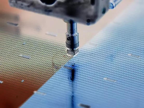
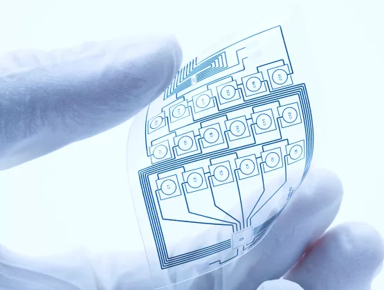
SEMI’s annual FLEX Conference Exhibition returns to Monterey, California, February 18-21, 2019, bringing together nearly 100 speakers on the major developments at the leading edge of printed/flexible/hybrid sensors and electronics technology.The maturing technology for smarter sensors, in a wider range of flexible formats, is enabling new opportunities across a wide range of applications, from healthcare to agriculture. And that means sensor suppliers need to connect with a broader range of users to build the next generation of innovative outside-the-box solutions. SEMI gathers the flexible/hybrid integration supply chain, leading researchers and potential customers at this annual event to help advance the sector.Collaborative efforts for sensors emerging markets: global health, faster crop development, military monitoringThere’s huge potential for smarter, more accessible sensor systems to detect infectious diseases and aid decision-making for community health workers around the globe, but new technologies and manufacturing methods alone will not be enough to meet the needs of these resource-constrained environments, argues Arunan Skandarajah, program officer at the Bill and Melinda Gates Foundation. He’ll introduce the foundation’s funding and partnering priorities for sensing and imaging for diagnostics and decision support and discuss potential paths forward for development.Recent advances in plant genomics and high-throughput phenotyping have big potential to enable faster development of crop varieties that better withstand adverse conditions – but that will depend on getting fast feedback from sensor data from the field. There’s immediate need for robust, high-efficiency, low-cost sensor technologies to collect on-the-ground microclimate and resource-use data from tractor-based sensors to field scanners, says Nadia Shakoor, Danforth Plant Science Center. She’ll discuss the sensors researchers need to develop high-yielding, energy- efficient crops that are resilient to variable climates.Military interest in biosensor patches to monitor human physiology and performance, and other sensor solutions for flexible imaging and point-of-care diagnostics, are also drivers of collaborative research between industry and universities. The Nano-Bio Materials Consortium (NBMC), a SEMI strategic association partnership with the Air Force Research Lab, will offer a workshop to discuss its potential needs, and how to get involved in its development program to create an integrated suite of nano-bio materials and production technology. Progress in scaling printed/hybrid flexible electronics manufacturing technologyThe maturing manufacturing supply chain continues to make progress towards scaling volume manufacturing of higher performance products, with recent innovations in materials and assembly technologies.Cal Poly researchers will report results from the recent FlexTech benchmark study of the flexible hybrid electronic industry. The study looks at the current state of maturity of the technology, its manufacturing processes, and its main applications while projecting the roadmap for future development. The study covers passives, sensors, batteries, antennas, speakers, PV and energy harvesting, and flexible hybrid integration.Catch up on new process development capabilities and recent work at the NextFlex Flexible Hybrid Electronics Manufacturing Institute’s San Jose Technology Hub for prototyping and pilot manufacturing. The institute has been adding engineers and projects as it looks towards the next generation of technology for sector growth. Innovations in scalable assembly of thin die on flexible substratesSeveral companies will update on recent progress developing solutions for the industrial-scale, high-yield assembly of fragile thinned die on to flexing substrates. American Semiconductor reports new automated assembly capacity for flip chip die attach and interconnect for devices with up to 100 I/Os and 100um pitch pads. The company also notes that it now has flexible Bluetooth ICs from two major suppliers available in semiconductor-on-polymer chip-scale packages, finally enabling improved wireless capacity for flexible hybrid systems.CEA-Leti will present its latest developments in flip chip bonding of thin bare die on flex. It uses gold stud bumps on the die, with 150°C thermocompression bonding to PEN Film. The researchers have also developed a wafer-level die process that thins and encapsulates die before removing them from the carrier wafer. systeMECH will also present its results for direct die placement of 300nm die on flexible polyester. Innovations in materials for easier processing, higher performanceDevelopments in substrates and processing may now enable use of photonics for laser patterning and flash curing on flexible substrates. Brewer Science will report developments on new polymers that can be quickly and cleanly etched with the mid-UV wavelengths commonly used for laser drilling and etching on printed circuit boards, bringing this improved performance to printed electronics as well. The polymers can be processed at less than 200°C with desirable qualities for substrates, adhesives, protective layers and the like for many electronics applications.Novacentrix will update on improvements in photonic curing equipment for fast heating to enable the use of high-temperature solders without damaging low-temperature substrates. Atotech will report results from its multiyear initiative to develop lower temperature solder pastes for better performance than SAC-based materials on a variety of substrates. Printed graphene and carbon nanotubes find applications in sensors and RF devicesBonbouton will introduce its commercial smart insole using a printed graphene sensor to monitor skin temperature to detect early signs of foot ulcers in diabetic patients. The company inkjet-prints graphene oxide followed by thermal reduction to fabricate graphene supercapacitor electrodes for temperature and pressure sensing.C2Sense will update on its development of carbon nanotube gas sensors to monitor food condition to prevent waste. The sensitized carbon nanotubes selectively detect ethylene from fruit or ammonia from chicken to accurately track the condition of the foods as they pass through the supply chain. Georgia Tech will report results of printing not only sensors from carbon nanotube ink but even RF and mm-wave diodes and transistors for high-frequency, long-range, low-cost RFIDs. Innovations in display materialsMaterials for flexible displays continue to see innovations – from solutions for foldable displays to plenty of new options for improved transparent conductive films and force-sensitive films. Solotech will introduce a cross-inked polymer that it says offers both high hardness and excellent foldability as a reliable covering for foldable/bendable displays. Atotech will describe its development of selective electroless copper deposition for metal mesh and TFT electrode patterns for touch screens to eliminate the need for costly mask and etching steps after deposition. Chasm Advanced Materials suggests hybrids of the conductive metals and carbon nanotubes offer a promising alternative for flexible transparent conductive films.C3Nano reports on nanowire ink, fused after printing, for flexible transparent conductors. Peratech will report on its printable pressure touch technology that it describes as high-resolution and low-cost for better localized, force-sensitive touch. Jabil will share the results of its evaluations of five of the available printed force-sensitive sensors. E Ink will introduce new capabilities for its electrophoretic display technology – it’s now possible to write on it with a magnetic stylus, and there’s a variable transmission version for electronic windows. Next generation technologies from universities and startupsResearchers from major research institutions and startups will talk about developments in flexible/printed/hybrid electronics including innovations in biological/electronics interfaces, via skin or neurons, and demonstrations of piezoelectric and better stretchable circuits. Emerging technologies for biosensors and human/machine skin interfaces Georgia Tech researchers will detail their electrical interface with human skin for wireless control of a remote-control car and a wheelchair by electrical signals from the body. They’ve developed a flexible elastomer skin patch patterned with thin film metal/polymer nanostructures made by CMOS processes, and metal pads compatible with conventional reflow soldering. Other Georgia Tech researchers will report their work on better cochlear implants made of encapsulated polymer printed with conductive microcoils for pulsed micro-magnetic stimulation that can focus more tightly on specific areas of auditory neurons. Seoul National University will introduce its flexible organic artificial nerves that can activate an insect’s leg muscle. Researchers there have devised a pressure sensor connected to a ring oscillator that converts the pressure signal into voltage pulses, which are then integrated by a transistor into a signal that replicates a post-synaptic current to communicate with the biological nerves.Epicore Biosystems will report on its advances in manufacturing and packaging technology that enable its skin-interface electronics and microfluidics systems in thin stretchable format to continuously monitor electrical, acoustic and biochemical signals. The technology is now entering commercial development with industrial partners. GE Global Research will update on its field testing of sweat-sensing devices to monitor hydration. Emerging technologies for piezoelectric actuators and improved stretchable sensors and circuits PARC will report on audio speakers made of PVD piezoelectric film on polyimide with inkjet-printed flexible hybrid operating circuits, and Novasentis will talk about its piezoelectric electroactive polymer for different kinds of vibrations for wristband notifications. UTC will share its learnings from deploying large numbers of stretchable flexible hybrid sensors conformably over large areas on aerospace and infrastructure assets to sense temperature, vibration, strain and damage for critical safety.The Air Force Research Lab reports promising results for stretchable circuits made with liquid metals, which maintain their high conductivity even when stretched. Silent Sensors will discuss its printed flexible manufacturing technology for low-cost, stretchable energy storage and piezoelectric energy harvesting for monitoring the condition of automobile tires.By Heidi Hoffman, senior director of technology community marketing, SEMI
Read More