downloadGroupGroupnoun_press release_995423_000000 copyGroupnoun_Feed_96767_000000Group 19noun_pictures_1817522_000000Member company iconResource item iconStore item iconGroup 19Group 19noun_Photo_2085192_000000 Copynoun_presentation_2096081_000000Group 19Group Copy 7noun_webinar_692730_000000Path
Skip to main content
Default Banner Image

Brewer Science

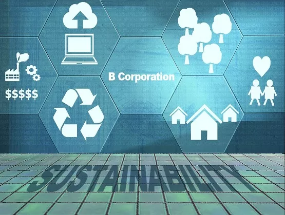
Becoming a Certified B Corporation™ comes with many benefits, most of them extending beyond the walls of the company and into the hands of employees, community members, and industry partners. The designation makes the meticulous and rigorous process to certification well worth the endeavor. In 2021, Brewer Science announced that it’s the first company in the semiconductor industry to become a Certified B Corporation. Our journey to become a Certified B Corporation inspired us to share our top five reasons for meeting the high standards the designation sets for both environmental and social responsibility. 1. Pave a pathway for continuous improvement B Lab™, the certifying organization for B Corps, believes in continuous improvement, and B Corps must create an improvement plan to demonstrate the areas of social and environmental performance they focus on in the coming years. Brewer Science will hold B Corp certification for three years before submitting to a renewal process. In order to be recertified, a company must score higher on recertification than on the previous certification. The assessment evaluates all facets of the company, and it’s a learning process to help the company target and identify ways to improve business practices. Brewer Science has already identified improvement areas for the recertification. We’ve implemented several human resource initiatives that are not written into policy yet, such as flexible and expanded work options. Additionally, we have expanded our use of a cloud-based learning platform to provide employees with more training options and performance conversations held quarterly instead of annually. Brewer Science scored many points for community involvement and charitable giving. However, we are still expanding community engagement by supporting or donating to a new local organization each month. Brewer Science became Certified Employee-Owned in 2020, but since it was the first year of the ESOP and shares were not yet dispersed, B Lab didn’t fully recognize the program. 2. Share the values of your stakeholders In 2006, Brewer Science started externally reporting environmental, safety, and health performance every year through its annual Corporate Sustainability Report in order to be transparent with customers, suppliers, and employees. The impact of this report on all of our stakeholders motivated us to pursue other ways to promote sustainability and inclusion as a shared asset for our customers and suppliers. In 2016, Brewer Science became GreenCircle Certified Zero Waste to Landfill, an annual certification that we have achieved every year since then. Certified B Corporations are businesses that meet the highest standards of verified social and environmental performance, public transparency, and legal accountability to balance profit and purpose. The standard is highly respected standard, in part because of B Lab’s rigor with the questionnaire and certification process. Not only does becoming a B Corp show your stakeholders that you care, and that you are walking the walk, but it also allows you to show how much your company cares through your B Corp Impact Area. Brewer Science pursued the impact area of environmentally innovative manufacturing, a category that required detailed evidence of how Brewer Science manages the manufacturing waste and minimizes its carbon footprint. The B Impact Area Scores reflect the five areas where the business excels. 3. Be competitive in an industry that demands sustainability and social responsibility Sustainability is of growing importance in the semiconductor industry. A company can convey its commitment to sustainability by becoming a Certified B Corp. The B Impact Assessment requires benchmarking to other companies in the industry in areas of social concern, such as sustainability, inclusion, and diversity. While benchmarking was nearly impossible for Brewer Science since we rank high as an innovator in these areas, we were able to not only set the benchmark for ourselves, but other industry partners who pursue B Corp certification in the future through our collaboration with B Lab. 4. Connect with a community that cares Becoming a Certified B Corporation instantly opens companies up to a network of other B Corps across the world. The more than 4,000 B Corps in 150 industries and 74 countries enables makes it easy to network in the areas such as environmental initiatives, attracting top talent, and even just using business as a force for good in the semiconductor industry. Knowing that a business is actively trying to make a positive social change will help attract top talent looking to find meaning in their careers. B Corp certification validates a company’s employee-centric culture, which can help beef up employee retention. What’s more, an exclusive job posting board called B Work, sponsored in part by B Lab, helps connect job seekers with companies that share their values. Employees are connected through an exclusive B Corporation community platform, B Hive, enabling them to collaborate and share ideas with other B Corp employees. There is also a section within the B Hive where other B Corps can share benefits with other B Corp member employees. With such a diverse range of companies that are Certified B Corps, shared benefits can include anything from discounted clothing to travel deals or even free consultations. Additionally, employees of B Corporations can collaborate on local recycling events and community engagement. 5. The bottom line Companies don’t pursue the Certified B Corp designation to drive improvements to their bottom line. Yet by sharpening their focus on environmentally sustainable initiatives and diversity and inclusion, most companies could indirectly see significant return on investment. For example, having a pathway for continuous improvement, sharing the values of your stakeholders, being competitive in the industry, and connecting to clientele and employees that value social responsibility all enable your business to grow. In the long run, becoming certified as a B Corp can save a company money by giving companies access to community data that provides insights into cost-effective ways to be more sustainable. Plus, the certification process helps companies identify wasteful spending. For more information about Certified B Corporations, and to get started on your company's application, visit the Certified B Corporation website. Jessica Albright is a content marketer at Brewer Science, Inc.
Read More
Understanding the significance of a B Corp™ comes down to measuring the success of a company in more than profits and ROI. Can global impact, sustainability, and social justice deliver value to stakeholders too? At Brewer Science, we boldly answered, “yes!” and launched our journey to becoming a Certified B Corporation™. A B Corp is a for-profit, corporate entity that seeks to positively impact society, the community, and the environment, in addition to generating profit. The concept is catching on. Today, there’s a worldwide network of almost 4,000 Certified B Corporations across 150 different industries and 74 countries. In May 2021, Brewer Science announced that we are the first company in the semiconductor industry to become a Certified B Corporation. As a chip industry trailblazer for this certification, Brewer Science wanted to share a little about its journey and answer questions often posed by its suppliers, customers, and competitors: Why would a company go through the exhaustive auditing process, how does it work, who does it involve, and what comes next? Why did Brewer Science seek to become a Certified B Corporation? Certified B Corporations are the forefront of a growing global movement of people using business as a force for good™. Certification demonstrates a spirited commitment to high standards of social and environmental performance, transparency, and accountability. “Certified B Corporation standards align with our mission of being a company of the people, by the technology, for the customer, to achieve fulfillment,” said Dr. Terry Brewer, Founder and CEO of Brewer Science. “Becoming a Certified B Corporation exemplifies our commitment to our mission to continuously evolve our global footprint to the benefit of our employees, community, and customers, adding unexpected value throughout the world.” Certified B Corporations are held accountable for environmentally friendly business practices, being inclusive, and promoting local businesses. Besides providing a social benefit to our suppliers, customers, and employees, the certification also gives Brewer Science extensive opportunities to grow the business in collaboration with other mission-driven companies and people. For example, as Certified B Corporations, companies can attend the B Climate Collective and work synergistically with other B Corp companies to advocate for social change. How did we become a B Corp? Brewer Science completed a meticulous assessment process conducted by B Lab™, which examined over 170 factors in reviewing Brewer Science’s customers and vendors, record of inclusion, community involvement, corporate governance, and environmental impact. B Lab also analyzed average employee tenure, charitable giving, energy savings plan, recycling policies, employee volunteer service, and employee upward mobility. The process of becoming a B Corp begins with a self-assessment that the company’s Board of Directors must certify and ends with a 90-minute review call during which B Lab reviews the company’s responses and the company presents supporting evidence. The entire process is rigorous, with the company winning and losing points based on various criteria. These points are factored into weighing its strength as a candidate, and also in identifying opportunities where the company can improve. B Corp status is granted when the company earns at least 80 out of 200 points. But, this is just the starting point of an ongoing process of growth and improvement to uphold the values of the B Corp into the future. The assessment is more than a scorecard. It’s a thorough inspection of every facet of the company and helps guide it in making changes, since every question in the B Impact Assessment must be supported by an explanation and real-life example. A key part of the certification requires choosing a Business Impact Area, which requires the company to prevent evidence of processes it has implemented to influence that area. This component counts for 29 of the 80 points required to achieve Certified B Corporation status. Brewer Science pursued the impact area of environmentally innovative manufacturing, requiring us to provide detailed evidence of how we manage waste in manufacturing and minimize our carbon footprint. We earned an Overall B Impact Score of 88.7. Brewer Science also addressed other areas in the B Impact Assessment such as our human resource initiatives, community involvement, commitment to helping underserved communities, and seeking minority-owned businesses–just to name a few. The assessment incudes the five B Impact areas where Brewer Science scored the highest. Who was involved in the B Corp process? Brewer Science assembled an internal B Corp task force team of directors from departments across the company to provide a cohesive and complete view of the company – a step that was necessary for us to meet the requirements of B Lab’s extensive auditing of the company. B Lab encourages the use of an outside consultant that serves as a liaison between the company and B Lab. Brewer Science’s internal B Corp task force team held bi-monthly meetings with its consultant for nearly a year to answer the hundreds of questions in the questionnaire and gather evidence to corroborate each claim. “It’s a very extensive, but very rewarding process,” said Karen Brown, Project Manager at Brewer Science, also known as the B Keeper by B Lab since she led the certification process within the company. "B Lab is very thorough with the process. It is detailed with what it means and what the questions stand for. It is firm with its requests to ensure that the certification is taken seriously.” What’s next on Brewer Science’s B Corp Journey? Brewer Science’s B Corp certification is valid for three years, at which we point we will apply for renewal – a process that will require us to score even higher than on the previous certification. B Lab stresses continuous improvement, and B Corps must create an improvement plan that spells out areas they will enhance in the coming years. Brewer Science has already identified improvement areas for the recertification. Several of our new human resources initiatives – such as flexible and expanded work options – have not yet been committed to policy. Additionally, we have expanded our use of a cloud-based learning platform to increase training options for employees and hold performance conversations quarterly instead of annually. As part of the assessment, Brewer Science won points for community involvement and charitable giving. However, we are expanding our community engagement by providing employees with a monthly charity or cause to support. Brewer Science became a Certified Employee-Owned company last year. Since 2020 marked the launch of our employee stock ownership plan (ESOP) and shares had not yet been dispersed, B Lab didn’t fully recognize the program. These are just a few examples of how we plan to earn more points during the recertification. At Brewer Science, we hope we can inspire other industry leaders to apply for certification. For more information about Certified B Corporations, and to get started on your company's application, visit the Certified B Corporation website. Jessica Albright is a content marketer at Brewer Science, Inc.
Read More
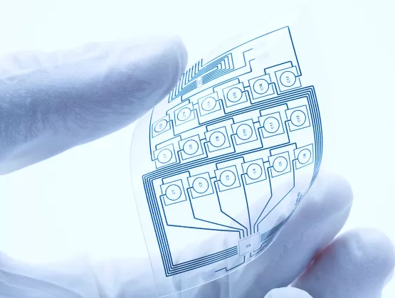
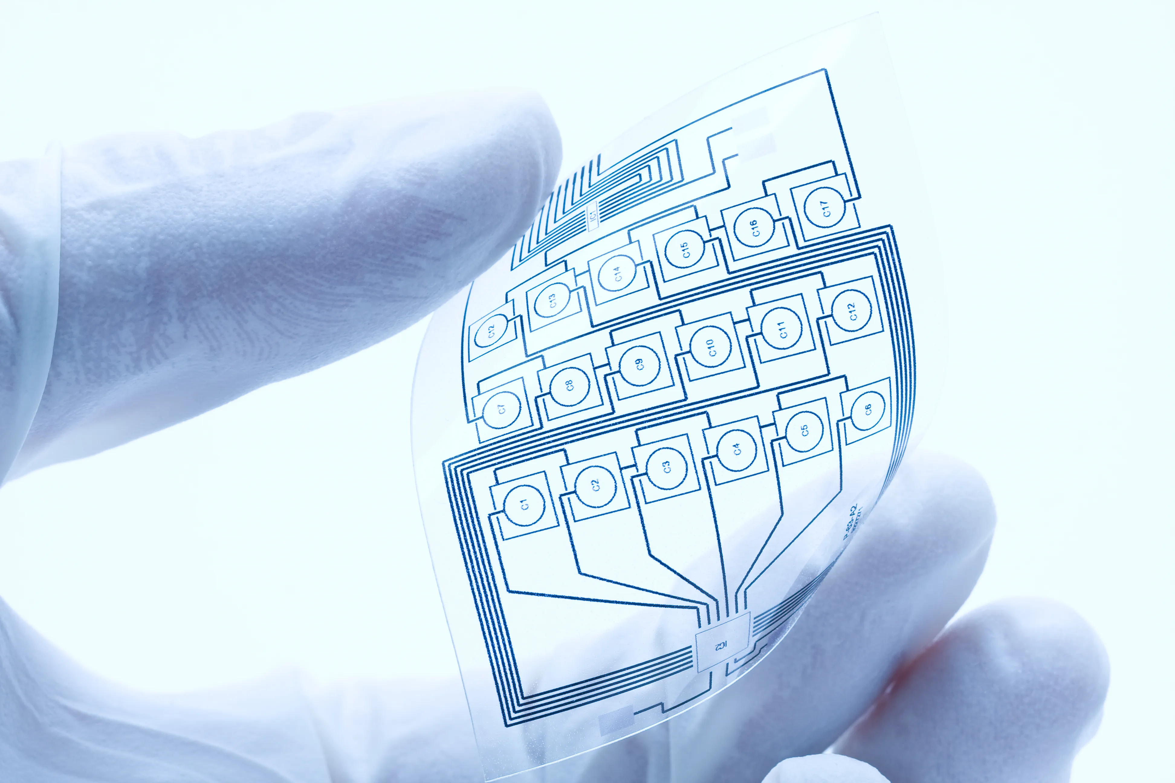
Flexible hybrid electronics (FHE) is innovation and modern technology at their best, giving rise to lighter, more malleable sensors that better conform to the human body while breeding new applications across a number of markets. For the semiconductor industry, FHE technology is enabling the development of a new generation of chips with the high performance, light weight, scalability, softness and flexibility usually seen in printed electronics. The technology is a boon to chipmakers, giving them novel ways to innovate for the Internet of Things (IoT) market.“The global printed electronics market is expected to garner 14.9% GAGR from 2018 to 2023,” said Stanley Wong, Director of Asia Business Development, Brewer Science, said in his presentation at FLEX Taiwan 2019 in late May. Representatives from industry, government, academia and research institutions gathered at the event in Taipei to explore flexible electronics innovation and growth opportunities.One shining star of FHE innovation is the foldable smartphone. So bright is the future of the bendable devices that not even recent trade tensions between the United States and China have dimmed prospects for the fledgling industry.“While the US-China trade war might slow down shipments of Huawei’s phones, the industry remains bullish on foldable phones,” said Stacy Wu, Principal Analyst at IHS Markit. “When the first generation of flexible AMOLED displays was launched in 2016, the rolling radius was 3mm and it could be folded 200,000 times.”For foldable phones, the 200,000 mark was a major milestone – the industry’s consensus standard for foldable phone display reliability. The industry reasoned that phones capable of being folded and unfolded 200,000 times without distorting color or images or the display itself cracking was a safe bet for consumer adoption. Earlier this year, both Samsung and Huawei announced foldable phones using the thin-film-display technology, ushering in the era of mass-market availability of the devices. Steve Chiu, Division Director for Electronics, IC package, Industrial Technology Research Institute (ITRI), believes that breakthroughs in the next generation of flexible AMOLED technology will allow thin films to be folded 100,000 times with a rolling radius up to 30mm and electric resistivity of less than 10 percent. The rolling radius of 30mm, 10 times higher than today’s phones, will give foldables a higher bending radius, while the lower electric resistivity will help maintain the brightness of the AMOLED panel after tens of thousands usages and extend the service life of foldable smartphones.The biggest challenge facing the foldable phone industry remains developing new materials that are flexible yet durable, stressed Francesco Lemmi, Business Development Director, Flexible Display, at DuPont. Today, the prevailing practice is to layer polyimide (PI) and hard coating on the display module. These stacked protective films replace traditional glass panels but present technical challenges related to impact resistance and the durability of the display as it is folded and unfolded over time.Smart clothing market is another hot market, with 33 percent global growth annually and revenue expected to reach US$ 3.26 billion in 2026. Yet for all the promise of smart clothing, reliability and accuracy remain a big challenge chiefly due to a lack of industry standards. Another gap is the unanswered question of whether consumers will embrace light and energy-efficient products.FLEX Taiwan 2019 speaker Satoshi Maeda of Toyobo is confident they will, pointing out that in the future consumers will enjoy a wide selection of comfortable smart clothing products and applications. The industry is still working to better understand how to develop human-machine interfaces, the essential seam between the human body (the outer layer of skin) and electronics, said Dr. Reinhold H. Dauskardt of Stanford University. Still, he sees great promise in an innovative somatosensory communications platform involving human skin. Human-computer interactions have historically been defined by human touch and vision (for example, typing at a computer keyboard and checking our monitor for the accuracy of our inputs). Dauskardt believes that, in the future, electrical impulses from the skin (conductance) will interact with signals from electronic devices to establish a more intimate human-machine interface that could be adapted one day to extend the visual and auditory abilities of humans.David M. Yeung, co-founder and CEO of Lionrock Batteries, pointed to another challenge in wearables: battery size. Today, large and heavy batteries account for 50 percent to 70 percent of the space in wearable devices, making many of the products too cumbersome to wear. Nanofiber lithium-ion batteries now under development can be as small as ultra-thin 2mm with a rolling radius of up to 20mm in radius and support for high electrical currents, significantly lightening their weight and improving comfort.Nardev Ramanathan, Lead Analyst, Digital Health and Wellness at Lux Research, predicts that, of all flexible electronics products, smart watches will win the largest market share and with the fastest rate of adoption. The devices will get a boost when they shrink as flexible batteries are integrated with the bands. The next wave of smart wearables will feature devices for exercise or medical monitoring. Already, FHE materials have led to advances in medical devices. One example is that smaller hearing aids are now possible thanks to flexible electronics and dressings used to promote skin regeneration, reduce wrinkles and remove scars.Gillian Ewers, VP Marketing at PragmatIC, sees fertile ground for FHE applications in IoT solutions. As FHE manufacturing costs drop, she believes IoT technologies will significantly deepen their penetration into a broad range of industries. For example, the number of electronic tags used in convenience stores worldwide will exceed 100 billion in 2025. Thinner than human hair and more durable than traditional wafers, these tags are expected to spawn a host of new business opportunities. FLEX Taiwan attracted more than 270 attendees from more than 30 fields including smart healthcare, e-paper, displays, system integration, automotive electronics, textiles, wearables, and avionics. On the first day of the event, industry, academia and research center representatives from the United States, Japan, China, Singapore and Taiwan gathered to discuss common goals on a range of FHE-related issues and deepen cross-regional cooperation. Like the FHE industry itself, SEMI-FlexTech remains focused on the future by strengthening cross-border cooperation to help manufacturers find killer applications and test profit-making models. For Taiwanese companies, the event will continue to provide insights on market trends, equipment, materials, advanced manufacturing technologies, product applications and new business opportunities, helping the organizations hone their competitive edge in the global market.Emmy Yi is a marketing specialist at SEMI Taiwan.
Read More
SEMI’s annual FLEX Conference Exhibition returns to Monterey, California, February 18-21, 2019, bringing together nearly 100 speakers on the major developments at the leading edge of printed/flexible/hybrid sensors and electronics technology.The maturing technology for smarter sensors, in a wider range of flexible formats, is enabling new opportunities across a wide range of applications, from healthcare to agriculture. And that means sensor suppliers need to connect with a broader range of users to build the next generation of innovative outside-the-box solutions. SEMI gathers the flexible/hybrid integration supply chain, leading researchers and potential customers at this annual event to help advance the sector.Collaborative efforts for sensors emerging markets: global health, faster crop development, military monitoringThere’s huge potential for smarter, more accessible sensor systems to detect infectious diseases and aid decision-making for community health workers around the globe, but new technologies and manufacturing methods alone will not be enough to meet the needs of these resource-constrained environments, argues Arunan Skandarajah, program officer at the Bill and Melinda Gates Foundation. He’ll introduce the foundation’s funding and partnering priorities for sensing and imaging for diagnostics and decision support and discuss potential paths forward for development.Recent advances in plant genomics and high-throughput phenotyping have big potential to enable faster development of crop varieties that better withstand adverse conditions – but that will depend on getting fast feedback from sensor data from the field. There’s immediate need for robust, high-efficiency, low-cost sensor technologies to collect on-the-ground microclimate and resource-use data from tractor-based sensors to field scanners, says Nadia Shakoor, Danforth Plant Science Center. She’ll discuss the sensors researchers need to develop high-yielding, energy- efficient crops that are resilient to variable climates.Military interest in biosensor patches to monitor human physiology and performance, and other sensor solutions for flexible imaging and point-of-care diagnostics, are also drivers of collaborative research between industry and universities. The Nano-Bio Materials Consortium (NBMC), a SEMI strategic association partnership with the Air Force Research Lab, will offer a workshop to discuss its potential needs, and how to get involved in its development program to create an integrated suite of nano-bio materials and production technology. Progress in scaling printed/hybrid flexible electronics manufacturing technologyThe maturing manufacturing supply chain continues to make progress towards scaling volume manufacturing of higher performance products, with recent innovations in materials and assembly technologies.Cal Poly researchers will report results from the recent FlexTech benchmark study of the flexible hybrid electronic industry. The study looks at the current state of maturity of the technology, its manufacturing processes, and its main applications while projecting the roadmap for future development. The study covers passives, sensors, batteries, antennas, speakers, PV and energy harvesting, and flexible hybrid integration.Catch up on new process development capabilities and recent work at the NextFlex Flexible Hybrid Electronics Manufacturing Institute’s San Jose Technology Hub for prototyping and pilot manufacturing. The institute has been adding engineers and projects as it looks towards the next generation of technology for sector growth. Innovations in scalable assembly of thin die on flexible substratesSeveral companies will update on recent progress developing solutions for the industrial-scale, high-yield assembly of fragile thinned die on to flexing substrates. American Semiconductor reports new automated assembly capacity for flip chip die attach and interconnect for devices with up to 100 I/Os and 100um pitch pads. The company also notes that it now has flexible Bluetooth ICs from two major suppliers available in semiconductor-on-polymer chip-scale packages, finally enabling improved wireless capacity for flexible hybrid systems.CEA-Leti will present its latest developments in flip chip bonding of thin bare die on flex. It uses gold stud bumps on the die, with 150°C thermocompression bonding to PEN Film. The researchers have also developed a wafer-level die process that thins and encapsulates die before removing them from the carrier wafer. systeMECH will also present its results for direct die placement of 300nm die on flexible polyester. Innovations in materials for easier processing, higher performanceDevelopments in substrates and processing may now enable use of photonics for laser patterning and flash curing on flexible substrates. Brewer Science will report developments on new polymers that can be quickly and cleanly etched with the mid-UV wavelengths commonly used for laser drilling and etching on printed circuit boards, bringing this improved performance to printed electronics as well. The polymers can be processed at less than 200°C with desirable qualities for substrates, adhesives, protective layers and the like for many electronics applications.Novacentrix will update on improvements in photonic curing equipment for fast heating to enable the use of high-temperature solders without damaging low-temperature substrates. Atotech will report results from its multiyear initiative to develop lower temperature solder pastes for better performance than SAC-based materials on a variety of substrates. Printed graphene and carbon nanotubes find applications in sensors and RF devicesBonbouton will introduce its commercial smart insole using a printed graphene sensor to monitor skin temperature to detect early signs of foot ulcers in diabetic patients. The company inkjet-prints graphene oxide followed by thermal reduction to fabricate graphene supercapacitor electrodes for temperature and pressure sensing.C2Sense will update on its development of carbon nanotube gas sensors to monitor food condition to prevent waste. The sensitized carbon nanotubes selectively detect ethylene from fruit or ammonia from chicken to accurately track the condition of the foods as they pass through the supply chain. Georgia Tech will report results of printing not only sensors from carbon nanotube ink but even RF and mm-wave diodes and transistors for high-frequency, long-range, low-cost RFIDs. Innovations in display materialsMaterials for flexible displays continue to see innovations – from solutions for foldable displays to plenty of new options for improved transparent conductive films and force-sensitive films. Solotech will introduce a cross-inked polymer that it says offers both high hardness and excellent foldability as a reliable covering for foldable/bendable displays. Atotech will describe its development of selective electroless copper deposition for metal mesh and TFT electrode patterns for touch screens to eliminate the need for costly mask and etching steps after deposition. Chasm Advanced Materials suggests hybrids of the conductive metals and carbon nanotubes offer a promising alternative for flexible transparent conductive films.C3Nano reports on nanowire ink, fused after printing, for flexible transparent conductors. Peratech will report on its printable pressure touch technology that it describes as high-resolution and low-cost for better localized, force-sensitive touch. Jabil will share the results of its evaluations of five of the available printed force-sensitive sensors. E Ink will introduce new capabilities for its electrophoretic display technology – it’s now possible to write on it with a magnetic stylus, and there’s a variable transmission version for electronic windows. Next generation technologies from universities and startupsResearchers from major research institutions and startups will talk about developments in flexible/printed/hybrid electronics including innovations in biological/electronics interfaces, via skin or neurons, and demonstrations of piezoelectric and better stretchable circuits. Emerging technologies for biosensors and human/machine skin interfaces Georgia Tech researchers will detail their electrical interface with human skin for wireless control of a remote-control car and a wheelchair by electrical signals from the body. They’ve developed a flexible elastomer skin patch patterned with thin film metal/polymer nanostructures made by CMOS processes, and metal pads compatible with conventional reflow soldering. Other Georgia Tech researchers will report their work on better cochlear implants made of encapsulated polymer printed with conductive microcoils for pulsed micro-magnetic stimulation that can focus more tightly on specific areas of auditory neurons. Seoul National University will introduce its flexible organic artificial nerves that can activate an insect’s leg muscle. Researchers there have devised a pressure sensor connected to a ring oscillator that converts the pressure signal into voltage pulses, which are then integrated by a transistor into a signal that replicates a post-synaptic current to communicate with the biological nerves.Epicore Biosystems will report on its advances in manufacturing and packaging technology that enable its skin-interface electronics and microfluidics systems in thin stretchable format to continuously monitor electrical, acoustic and biochemical signals. The technology is now entering commercial development with industrial partners. GE Global Research will update on its field testing of sweat-sensing devices to monitor hydration. Emerging technologies for piezoelectric actuators and improved stretchable sensors and circuits PARC will report on audio speakers made of PVD piezoelectric film on polyimide with inkjet-printed flexible hybrid operating circuits, and Novasentis will talk about its piezoelectric electroactive polymer for different kinds of vibrations for wristband notifications. UTC will share its learnings from deploying large numbers of stretchable flexible hybrid sensors conformably over large areas on aerospace and infrastructure assets to sense temperature, vibration, strain and damage for critical safety.The Air Force Research Lab reports promising results for stretchable circuits made with liquid metals, which maintain their high conductivity even when stretched. Silent Sensors will discuss its printed flexible manufacturing technology for low-cost, stretchable energy storage and piezoelectric energy harvesting for monitoring the condition of automobile tires.By Heidi Hoffman, senior director of technology community marketing, SEMI
Read More