downloadGroupGroupnoun_press release_995423_000000 copyGroupnoun_Feed_96767_000000Group 19noun_pictures_1817522_000000Member company iconResource item iconStore item iconGroup 19Group 19noun_Photo_2085192_000000 Copynoun_presentation_2096081_000000Group 19Group Copy 7noun_webinar_692730_000000Path
Skip to main content
Default Banner Image

Atomic Layer Deposition

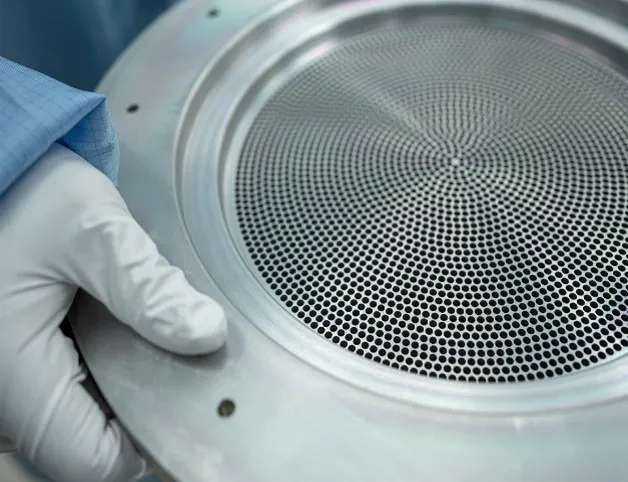
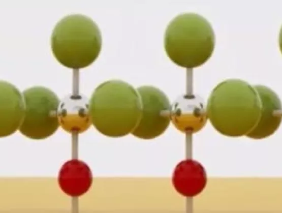
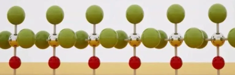
Atomic layer deposition (ALD) and atomic layer etching (ALE) are transforming the way semiconductors are built—layer by layer, atom by atom. These atomic-scale processes are essential to scaling future transistors, improving memory, and enabling next-generation device architectures.SEMI spoke with Sergei Ivanov, Business Technology Director of Metallics R D and Balaji Kannan, Business Technology Director of Dielectrics R D and from Merck KGaA, Darmstadt, Germany to learn about their latest material innovations. At the company’s Electronics business, materials scientists and process engineers are advancing atomic-scale engineering to address some of the semiconductor industry’s toughest challenges. From novel deposition chemistries to next-generation etch techniques, their work is helping to enable future logic, memory, and specialty devices.Pushing the Boundaries of ALD Precursor ChemistryAtomic Layer Deposition (ALD) remains a cornerstone technology for scaling transistors and enabling new architectures. Materials scientists at Merck KGaA, Darmstadt, Germany are exploring novel precursors that enhance film quality, streamline processes, and expand the operational window for complex structures:One area of focus is next-generation hafnium and zirconium precursors. “These advanced high-k dielectrics offer better thermal stability, improved step coverage, and reduced impurities while achieving higher k-values,” Sergei Ivanov explained. “Such attributes are essential for logic and memory devices that demand reliable dielectric performance with minimal defect density.”Another important development is area selective deposition (ASD). Merck KGaA, Darmstadt, Germany’s small-molecule inhibitor solutions reduce the need for advanced patterning in narrow dimensions and 3D geometries, enabling cost-effective and simpler integration for leading-edge nodes. Their selective co-reactants platform leverages digitalization techniques including multivariate analysis, digital twin technology, and machine learning to accelerate process development for critical ASD applications. This approach facilitated industry-first adoption of ASD in high volume manufacturing and enables an ever-expanding toolbox of OEM processes for ASD of high-k, Ti, Mo, Si and other thin films.Merck KGaA, Darmstadt, Germany is also broadening the scope of ALD chemistries across the periodic table. “As our customers encounter new technical challenges, we continue to expand our R D scope across new elements and ligands. Examples include europium, lanthanum, scandium, and cerium dopants with improved electrical properties, niobium and vanadium precursors for deposition of nitride and oxide films with reduced impurities and improved ALD performance, and high-performance nickel MILC solutions are finding their way out of our labs and into customer roadmaps at an ever-accelerating pace,” said Sergei Ivanov.The company’s role in molybdenum chemistry is another example. Merck KGaA, Darmstadt, Germany is a key producer of molybdenum precursors including MoO2Cl2 with industry-leading quality, density, and container utilization. The company offers MoCl5 with advanced trace impurity control paired with innovative container technology. The company’s next-generation organic metallic molybdenum precursors incorporate novel ligands that contribute to critical gains in device performance.Merck KGaA, Darmstadt, Germany’s work with organosilane precursors is also opening new possibilities. “For gate-all-around (GAA) transistor technology, precursors incorporating novel bonding structures enable highly conformal dielectric films with excellent electrical and physical properties, even in complex 3D geometries. At the same time, organosilane chemistries designed to increase silicon incorporation during deposition are supporting high-growth-rate oxides for gapfill applications, delivering the thick films required with greater throughput,” said Balaji Kannan. “Together, these innovations highlight how tailored precursor design can address both scaling challenges and manufacturability in next-generation devices.” Driving Selective and Sustainable Atomic Layer Etching (ALE)“Precision in etching is as critical as deposition. Our innovations in ALE are designed to provide ultra-selective, low-damage material removal, which is increasingly vital as device geometries become finer and more complex,” Sergei Ivanov shared. One example is metal-free ligand exchange ALE for high-k materials, where Merck KGaA, Darmstadt, Germany’s research into etching HfO₂, ZrO₂, and HfZrO₄ showcases a novel metal-free approach. This technique enables accurate and damage-minimized etching of high-k dielectrics, which is essential for integrating advanced transistors and memory stacks.These advancements address industry-wide concerns regarding pattern fidelity, material selectivity, and plasma-induced damage, ensuring greater process control and extending the lifetimes of devices.Looking AheadMerck KGaA, Darmstadt, Germany’s strategic commitment to semiconductor innovation includes ongoing R D efforts that reflect the vision of its Electronics business: providing material-centric solutions to the industry’s most complex integration and performance challenges. Whether advancing front-end device scaling or developing breakthrough materials for emerging applications, the Electronics business of Merck KGaA, Darmstadt, Germany is committed to shaping the materials roadmap for a more connected, intelligent, and efficient world.James Lam is Business Development Manager at SEMI Europe.
Read More
With each transition to a new technology node, fab requirements for metal and particle contamination become more stringent, posing challenges for existing coating methods such as anodization or plasma spray that may not provide complete protection against contamination especially on critical chamber components with complex geometry. SEMI spoke with Beneq business executive Sami Sneck about common metal and particle contamination issues with critical chamber components, coating methods to protect against corrosion, and properties to look for when selecting the optimal protective coating solution. Sneck discussed the unique benefits of atomic layer deposition (ALD)anti-corrosion coatings with Aluminiumoxide (Al2O3) and Yttrium Oxide (Y2O3) and offered recommendations on how to work with original equipment manufacturer (OEM) partners to design, test and implement an ALD coating solution for semiconductor equipment. To learn more, visit Beneq at its digital booth at SEMI Technology Unites Global Summit, available on-demand until March 26, 2021. Registration is open. SEMI: How does ALD compare with other coating methods such as anodization and plasma spray? Sneck: ALD enables conformal dense and pinhole-free coatings on complex shapes. We can deposit various ALD coating materials on parts made of various materials. All other coating techniques have limitations. For instance, anodization is conformal, but porous and is suitable for Al2O3 used for aluminum parts. Plasma Spray is a line-of-sight method and not conformal on complex shapes, such as holes in showerhead parts. SEMI: Which substrate materials work for ALD coatings? Sneck: In general, parts made of common metal materials, such as aluminum, stainless steel or titanium, all work well with ALD coatings. Commonly used ceramic materials work well with ALD too. Plastic materials need to be coated generally at a lower temperature, which limits the coating material selection, but materials such as Al2O3 can be applied as well. SEMI: What is the maximum coating thickness you can reach with ALD? Does this depend on the material? Sneck: Yes, indeed. The maximum coating thickness does depend on the material of the part that we are coating. Polymer materials for example, have a very large coefficient of thermal expansion, which limits the practical coating thickness to the 100-nanometer level. On metal and ceramic parts, coatings of several micrometers are possible too. Typically, ALD coating thickness on chamber components range from a few hundred nanometers to one micrometer. SEMI: Which aspect ratio can you coat with ALD? Sneck: Basically, ALD can coat aspect ratios of 1000:1, but this would be extremely slow. In practice, some of the most complex parts are showerhead parts with small holes. Typically, these have an aspect ratio of around 100:1, which is perfectly commercially feasible for ALD. An extreme example would be gas lines: In this case, the aspect ratio may be also around 100:1, but the physical distance from one end to the middle may be half a meter. In this respect, it is not practical to wait for gas diffusion to reach such a depth level. Instead, the gas lines can be coated by forcing the ALD precursor gas flow into the gas line parts. This works well but needs part-specific manifolds to guide the gases. SEMI: What is the lifetime of ALD coating compared to other coatings? Sneck: ALD coatings differ from other coatings a couple of ways. First of all, ALD coatings generate less particle contamination since they are non-porous. Secondly, and most importantly, ALD coatings can cover areas that other coatings cannot. What is considered the lifetime of a certain part depends on various factors. Ultimately, the lifetime needs to be confirmed by testing parts in actual process chambers by running a lot of wafers through the chamber and monitoring critical parameters such as particle level and yield. SEMI: If you have multiple shelves with parts in the reaction chamber, how does the shelf position affect the coating uniformity? Is center shelf better than top and bottom shelf? Sneck: Uniformity depends on many parameters, including the part geometry, part holder geometry, batch size and coating material. When the shelves supporting the parts are optimally designed and the gas flow is well-distributed to all shelves, all shelves from top to bottom show similar uniformity. SEMI: Is there any risk of cross-contamination? Sneck: Cross-contamination could potentially be caused by the parts themselves or by different coating materials. The batch setup is fixed in production use, which means the parts are the same in every batch. The only variation is that the batch may not be full in some cases, but then we do not fill the empty part of the batch with other parts that could cause contamination in order to prevent contamination from one part type to another. Cross-contamination from one coating material to another is not a usual concern but can be prevented by using dedicated reaction chambers for different coating materials. This is very easy to do with Beneq P800. Sami Sneck manages Beneq’s semiconductor part coating business. He joined Beneq in 2005 and since then has held various professional and management positions including product manager, application manager, director of ALD group, head of sales, and head of Asia. He earned his MSc degree in Chemical Engineering in 2001 from Helsinki University of Technology. Sneck has special expertise in Atomic Layer Deposition technology and business development. He has played a vital role in introducing various ALD production concepts and solutions to several industries ranging from jewelry to photovoltaics, electronics and semiconductors. Access the free webinar recording and discover the latest anti-corrosion coating solutions and the unique benefits of ALD (atomic layer deposition). This webinar is particularly helpful for process engineers, equipment engineers and others responsible for contamination control and equipment yield. Serena Brischetto is senior manager of Marketing and Digital Engagement at SEMI Europe.
Read More
International Women’s Day (IWD) is a global day celebrating the social, economic, cultural and political achievements of women. The day is not only the centerpiece of the movement for women’s rights but a unique opportunity to recognize the contributions of women to the semiconductor industry. The first International Women’s Day took place in 1911 when more than a million people in Austria, Denmark, Germany and Switzerland marched to demand equal rights for women including the right to vote and to protest employment sex discrimination. In 1977, the United Nations General Assembly invited member states to proclaim March 8 the UN Day for women's rights and world peace. In recent years, organizations and companies worldwide have sought to use IWD to celebrate the contributions of women to our homes, families, workplaces and communities. The IWD theme for 2021 is Choose to Challenge – a call to draw attention to women’s inequality. It’s also an excellent opportunity for all SEMI members to choose to challenge deep-rooted thinking and behavior in order to grow diversity and collectively commit to increasing the representation of women and women-owned businesses in the semiconductor industry. The double-edged challenge for the chip industry is to grow the ranks of women while retaining those now in the workforce. One in four women are considering leaving their workplaces or downshifting their careers due to work-life challenges stemming from COVID-19, SEMI noted in a recent blog highlighting the Women in the Workplace 2020 study by McKinsey Company and LeanIn.org. One in four! In 2021 it’s important for us to recognize and work to reverse this trend by taking time to encourage, support and celebrate women in the face of COVID-19. A shining example of the enormous contributions to semiconductor industry by women is Dr. Suvi Haukka, a pioneer of atomic layer deposition (ALD) technology. Thirty years ago, Dr. Haukka spied a small note on a university noticeboard that led to her pursuit of a long and highly distinguished career in our industry. The note was a job opportunity with ASM International to research ALD, a role she landed. Upon joining ASM, Dr. Haukka investigated the use of ALD for catalysis applications to modify porous high-surface area materials used in oil refining and polymerization. What was initially a niche application to modify the surfaces of microporous substances and silicon solar cells evolved over time to become a critical materials technology and manufacturing method for coating semiconductor wafers. Working systematically in the lab, Dr. Haukka and her coworkers made fundamental materials and manufacturing process discoveries that advanced ALD material science and manufacturing technologies. An accomplished inventor and technical contributor, Dr. Suvi Haukka was named ASM’s very first Fellow of the Technical Staff in 2018. “Being named an ASM Fellow was a huge moment that made me very, very proud,” Dr. Haukka said. “I have spent my entire professional career working with ALD, and I have been very fortunate to work with many talented colleagues at ASM. “Together we have dedicated ourselves to introducing ALD as a standard means of manufacturing in the semiconductor industry. I believe the award is in recognition of all the valuable work we’ve done over the years.” Dr. Haukka is ASM’s most prolific inventor with more than 100 patents to her name. Her remarkable contributions to the development of ALD chemistry and semiconductor manufacturing process technologies over her three-decade career have made her a highly respected, internationally recognized researcher in the semiconductor manufacturing industry. Bill Olson is the corporate responsibility and conflict materials lead at ASM International N.V. in Phoenix, Arizona. He graduated from the University of Wisconsin-Madison with a Ph.D. in Inorganic Chemistry. Bill has 23 U.S. patents and has published more than 40 technical articles. He can be reached via LinkedIn at www.linkedin.com/in/williamolson.
Read More
SEMI spoke with Dr. Mikko Söderlund, sales director for Beneq’s semiconductor business, about trends in Atomic Layer Deposition (ALD) applications. Söderlund shared his views ahead of his presentation at SEMI MEMS Imaging Sensors Summit, 25-27 September, 2019, at the WTC in Grenoble, France. Join us at the event to meet Beneq and other key industry influencers. Registration is open.SEMI: The Backside Illuminated (BSI) CMOS Image Sensors (CIS) market continues to experience steady growth. Which applications are currently driving market growth?Söderlund: BSI CMOS Image Sensor market continues to be driven by mobile, security, automotive and Internet of Things (IoT) applications – so there seems to be plenty of opportunities for BSI CIS market to grow further.SEMI: What is critical for advanced thin-film deposition methods to extract best electrical performance?Söderlund: It is critical to control the material properties of the deposited layer (such as charge density, resistivity or barrier property) and of course, film uniformity and conformality. Furthermore, controlling material interfaces is also important, especially for sensitive III-V materials. {% video_player "embed_player" overrideable=False, type='scriptV4', hide_playlist=True, viral_sharing=False, embed_button=False, width='350', height='197', player_id='12721134435', style='margin: 0px auto; display: block; float: right; margin-left: auto; margin-right: auto; width: 350px;' %} Coatings and material features based on existing standard techniques can be very expensive, or not feasible at all. What does Atomic Layer Deposition (ALD), as a thin film coating method, offer in particular?Söderlund: ALD offers dense, highly conformal and pinhole-free best-in-class functional layers for dielectrics, passivation, encapsulation and much more. As a gentle and precise layer-by-layer method, ALD is extremely well-suited for deposition of such performance critical layers over large surface areas such as a cassette of wafers.SEMI: Please describe the Atomic Layer Deposition (ALD) coating process. Söderlund: ALD is based on a self-limiting surface reaction controlled thin film deposition. During coating, two or more chemical vapors or gaseous precursors react sequentially on the substrate surface, producing a solid thin film (see schematic below). Most ALD coating systems use a flow-through traveling wave setup, where an inert carrier gas flows through the system and precursors are injected as very short pulses into this carrier flow. The carrier gas flow takes the precursor pulses as sequential waves through the reaction chamber, followed by a pumping line, filtering systems and, eventually, a vacuum pump.SEMI: What are the two leading edge ALD applications?Söderlund: Today’s leading-edge ALD applications are in logic (high-k/metal gate, multiple patterning) and memory (DRAM capacitor, 3D NAND). Within the More-than-Moore (MtM) markets, CIS and MEMS (actuators and sensors, RF) have been early adopters of ALD, and we also see ALD being introduced in GaN Power and RF, as well as photonics.SEMI: Give us one prediction about the opportunities offered by advanced imaging applications.Söderlund: The large diversity of imaging applications will continue to drive growth and innovation. For example, machine vision is expected to transform the imaging landscape. We see this as a big opportunity for advanced thin-film deposition methods such as ALD, provided that the tools are versatile enough to address the diverse manufacturing requirements.SEMI: What are your expectations for SEMI MEMS Imaging Sensors Summit and why do you invite your peers to attend? Söderlund: The summit brings together all key RF stakeholders in the MEMS and imaging sensors industry, and we are looking forward to a great event. It’s a special event for us as we are officially launching a new ALD cluster tool product specifically engineered for the MtM applications – so this brings great excitement that we want to share with the attendees.Dr. Mikko Söderlund is Sales Director for Beneq’s semiconductor business. He has more than 20 years of experience in product development, product management, technical sales and business development across the photonics, OLED, and semiconductor industries. Mikko received his Ph.D. in Micro- and Nanotechnology from the Helsinki University of Technology. Serena Brischetto is a marketing and communications manager at SEMI Europe.
Read More