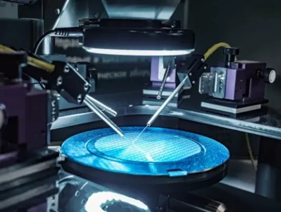
Artificial intelligence (AI) and high-performance computing (HPC) are driving unprecedented demand for data movement. As bandwidth requirements climb and conventional electrical interconnects encounter limitations in power consumption, latency and reach, silicon photonics, near-packaged optics (NPO), and co-packaged optics (CPO) are becoming increasingly important technologies for next-generation data centers.Much of the industry’s attention has focused on photonic device innovation. But demonstrating a high-performance photonic integrated circuit (PIC) is only part of the challenge. Turning these devices into products that can be manufactured reliably and economically at high volume requires a test infrastructure that can keep pace.This represents a significant shift. Semiconductor manufacturing has benefited from decades of refinement in automated electrical test. Silicon photonics adds an optical dimension that brings new requirements for fiber alignment, coupling efficiency, polarization management, and optical instrumentation—while still requiring conventional electrical characterization.As silicon photonics moves from development environments toward high-volume production, test becomes more than a quality gate. It is an integral part of the manufacturing strategy.An HVM-ready test solution requires a full complement of supporting hardware and software.Bringing precision optical alignment to productionOne of the most fundamental challenges is establishing a reliable optical connection to the device under test. Unlike electrical probing, where physical contact provides a relatively straightforward interface, optical testing depends on precisely coupling light into and out of very small structures.That coupling must be repeatable from device to device and wafer to wafer. Even small variations in fiber position or angle can affect insertion loss and measured optical performance, potentially making it difficult to distinguish actual device variation from variation introduced by the test setup.For this reason, high-volume testing requires automated alignment capabilities that can quickly locate the optical interface and optimize coupling. This can involve visual or image-based positioning to bring a fiber array unit close to the grating couplers, followed by area scans and gradient-search techniques to identify the optimal position via feedback loops – a technique typically referred to as “active alignment.” The process may also require optimization across six degrees of freedom—X, Y, and Z positioning plus three rotational axes—to maximize coupling efficiency and minimize channel-to-channel variation.The problem becomes more complex as optical interfaces add channels. Alignment must not simply maximize one channel's performance; it must produce consistent coupling across multiple channels. Rotational alignment, for example, can influence how evenly an optical beam overlaps multiple grating couplers. Other angular adjustments can affect both insertion loss and center wavelength.Polarization presents another variable. Because photonic structures can respond differently depending on the polarization state of incoming light, polarization must be characterized and controlled as part of a repeatable production methodology. Together, these requirements make alignment an active measurement and optimization process rather than a simple mechanical positioning step. The manufacturing challenge is to automate these functions without allowing alignment time to become a throughput bottleneck.Combining electrical and optical test without sacrificing throughputAlignment is only one part of the equation. A PIC may incorporate photodetectors, modulators, and other components requiring combinations of optical and electrical measurements. Typical characterization can include insertion loss, channel-to-channel uniformity, optical attenuation, photodetector responsivity, and wavelength-dependent behavior.Performing these measurements sequentially can add substantial test time. A more scalable approach is to integrate electrical and optical capabilities so that operations can occur concurrently wherever possible. For example, electrical alignment can occur before optical alignment, while continuity and other electrical tests may run during automated optical probe alignment rather than waiting for that process to finish. This type of parallelism becomes increasingly important as device complexity and test coverage grow.The same principle applies to optical instrumentation. Rather than treating each instrument as an isolated resource, high-volume environments benefit from integrated control of lasers, power meters, and other optical equipment, enabling parallel operation of multiple instruments or channels. Automated calibration and compensation are also important for maintaining measurement consistency as the test cell becomes more complex. Advantest’s development work in this area supports multiple optical instruments and parallel power-meter operation within a common test environment.The broader objective is familiar from semiconductor test: maximize useful test coverage while minimizing test cost. What changes with silicon photonics is the number of physical and measurement domains that must be coordinated to achieve it.Collaboration will be essential to ecosystem scalingNo single supplier controls all of the elements required for high-volume PIC test. The complete solution can span automated test equipment, wafer probing, optical positioning, fiber interfaces, optical instrumentation, device design, and manufacturing processes.That makes ecosystem collaboration particularly important. Test equipment providers need to work with probe and positioning specialists, photonic device developers, foundries, and manufacturers so the interfaces among these technologies function as an integrated production system rather than individual laboratory instruments.As an example, Advantest has collaborated closely with FormFactor to develop a wafer-level photonics test environment that combines electrical test instrumentation with wafer handling, optical instruments, and automated fiber alignment capabilities. The significance lies less in individual components than in the integration required to create a repeatable manufacturing workflow.As silicon photonics, NPO and CPO move toward broader adoption, these collaborative efforts will become increasingly important. The industry must develop practical test methodologies that accommodate evolving device architectures while delivering the repeatability, throughput, and economics expected of semiconductor manufacturing.Numerous photonics developments on the horizon will require broad industry effort to bring to fruition.The transition from promising photonic technology to high-volume commercial products will depend on more than advances in the devices themselves. Test must evolve alongside them. By treating optical alignment, electrical and optical measurement, automation, and ecosystem interoperability as parts of a single manufacturing challenge, the industry can build the infrastructure needed to bring silicon photonics fully into the era of high-volume production. About the AuthorDr. Clemens Leichtle is Senior Director and V93000 Photonic Business Lead for Advantest Corp. He has more than 25 years of experience in the semiconductor industry, with companies including Siemens, Agilent and Verigy, specializing in testing and developing respective application solutions for emerging technologies. For more than 15 years, he has been leading the V93000 Center of Expertise at Advantest; more recently, he co-led test solution development for silicon photonics and co-packaged optics targeting data center applications. Dr. Leichtle holds a Ph.D. in physics from the University of Ulm, Germany.