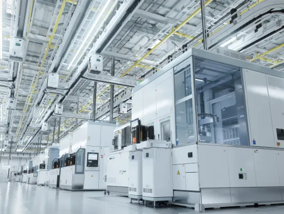
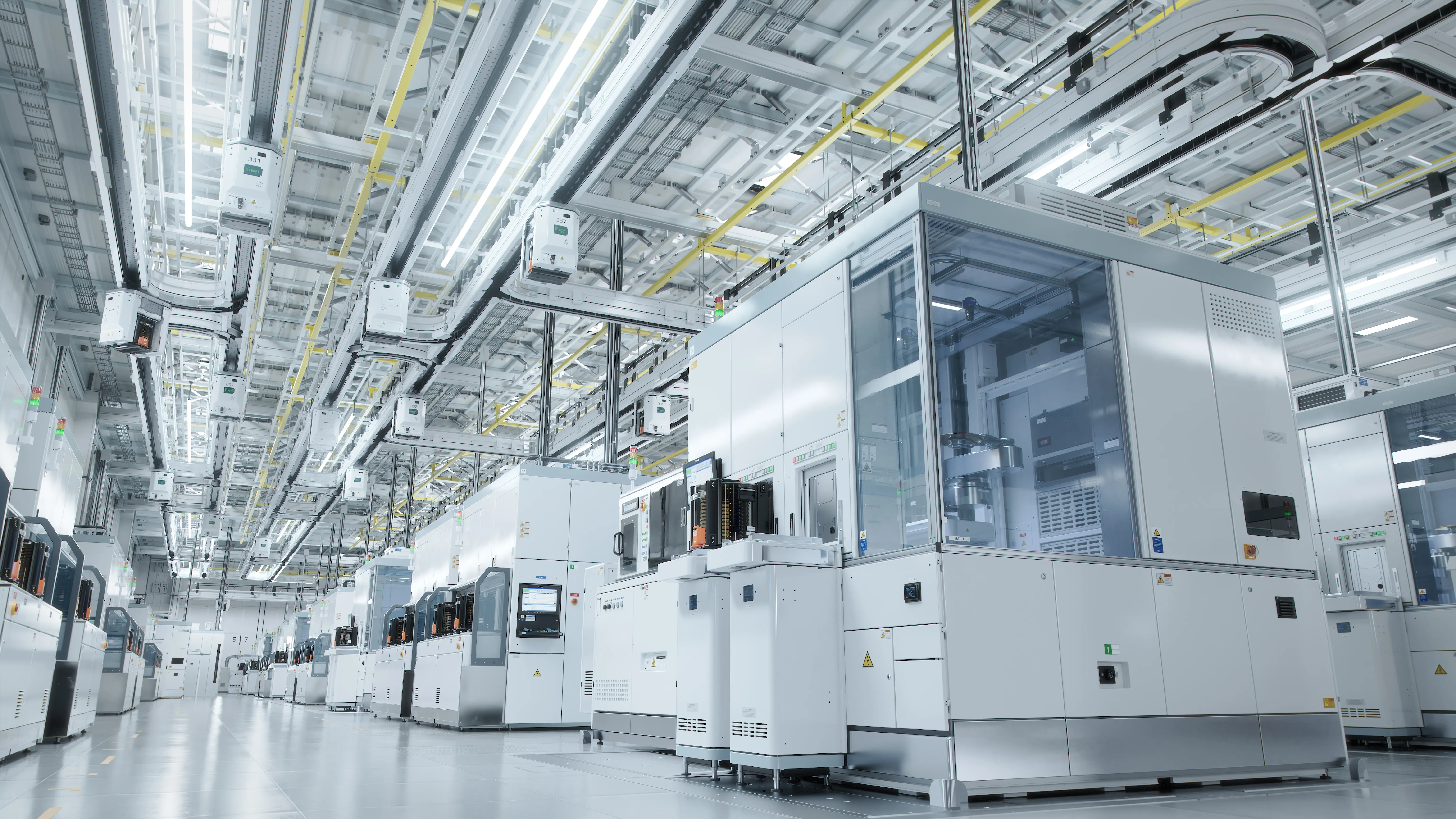
As semiconductor manufacturing advances through technologies such as advanced packaging, hybrid bonding, and increasingly complex process chemistries, the infrastructure supporting the fab is becoming more critical than ever. Yet many engineers and industry professionals remain unfamiliar with the systems collectively known as the “subfab.”In this blog, SEMI’s Mayura Padmanabhan spoke with Ilya Zabelinsky, founder of the International SubFab Research Labs (ISRL), about the growing importance of subfab infrastructure, the industry’s biggest challenges, and opportunities for collaboration, sustainability, and standards development.Padmanabhan: For readers who may be unfamiliar with the term, what is the subfab and why is it a critical part of semiconductor manufacturing?Zabelinsky: Linguistically, the term subfab refers to something underneath the fab. In many modern semiconductor factories, it is literally the floor below the cleanroom. However, the definition is much broader than a location. The subfab can include spaces below, above, or around the fab, and in some cases even systems located within the cleanroom itself.At its core, the subfab encompasses the equipment, technologies, and systems that support manufacturing. These include vacuum pumps, gas abatement systems, chillers, temperature control systems, chemical and gas distribution systems, and waste management infrastructure. While these systems often operate out of sight, they are essential to enabling the manufacturing processes that occur in the fab.“Subfab is a very broad definition of systems, equipment, technologies, and systems of systems that support manufacturing.”Padmanabhan: What are the most important subfab systems and concepts that every semiconductor professional should understand, even if they don’t work directly in facilities or operations?Zabelinsky: I generally group subfab systems into three major categories. The first includes equipment that is effectively part of the manufacturing tool itself but may be too large, noisy, or vibration-sensitive to sit inside the fab. Examples include vacuum pumps, chillers, heaters, RF generators, and electrical systems. Without these components, many semiconductor tools simply cannot operate.The second category includes systems that supply the process. These are the gas and chemical delivery systems that provide materials used in deposition, etch, lithography, CMP, and other manufacturing processes. Delivering materials at the proper purity, pressure, flow rate, and temperature is essential for yield, process control, and safety. The third category includes systems that remove what manufacturing leaves behind, including exhaust systems, waste streams, abatement systems, and cooling infrastructure. I often compare these systems to the human body’s digestive system. People rarely think about it when everything is functioning properly, but when it stops working, nothing else matters. Subfab systems play a similar role in semiconductor manufacturing. Padmanabhan: You recently delivered the Subfab 101 course in partnership with SEMI University, which sold out. What do you think resonated most with participants?Zabelinsky: Interest in subfab technologies has grown dramatically over the last few years. When I launched the ISRL initiative several years ago, there were very few publicly available resources on the topic. Today, there are more articles, videos, images, and technical discussions available, reflecting a growing awareness of how important these systems are to semiconductor manufacturing.Despite that increased awareness, many professionals still only see a small piece of the overall picture. Engineers may work with a pump, an abatement system, or a facility network without fully understanding how everything connects together. The course helped participants understand the broader ecosystem, including fab layouts, system interactions, technology evolution, and the role that subfab infrastructure plays in enabling manufacturing. For many attendees, it was the first time they could see how all of these systems function as a complete integrated environment.Padmanabhan: As fabs become more advanced, what new challenges are emerging in the subfab? Where do you see the greatest opportunity for improvement?Zabelinsky: One of industry’s biggest challenges is that we still do not fully understand what happens after materials leave the process chamber. While we understand many fundamental principles, there are still significant unknowns related to chemical reactions, particle formation, material behavior, and transport phenomena inside the systems that support semiconductor manufacturing.Without deeper scientific understanding, we often compensate by adding more equipment, consuming more energy, and relying on larger volumes of support resources such as purge gases. The opportunity lies in better understanding the underlying physics and chemistry so we can develop more efficient solutions. At the same time, many subfab systems continue to follow design approaches that were established decades ago. As advanced packaging, hybrid bonding, and new manufacturing techniques become more widespread, the industry has an opportunity to challenge long-standing assumptions and develop entirely new approaches to subfab design.“The first challenge is understanding the physics and chemistry of what the subfab deals with. The second is breaking paradigms and going after new concepts.”Padmanabhan: You founded ISRL to address challenges in this space. What inspired you to start ISRL, and what role does the organization play in advancing subfab knowledge, innovation, and industry collaboration?Zabelinsky: Throughout my career, I saw significant investments made in new transistor architectures, process technologies, materials, and manufacturing equipment. However, comparatively little effort was dedicated to understanding what happens to materials after they leave the process chamber or how those materials should be handled, treated, recycled, or neutralized. As semiconductor processes become more complex, these challenges become increasingly important.That realization led to the creation of the International SubFab Research Labs. The vision is to establish a collaborative environment where universities, chipmakers, equipment suppliers, material providers, and researchers can work together to better understand material behavior and develop next-generation subfab technologies. Ultimately, ISRL aims to provide infrastructure capable of replicating high-volume manufacturing conditions so that new concepts can be researched and validated without disrupting production fabs, where the primary focus must always remain on yield, quality, and output.Padmanabhan: Sustainability is becoming a major priority for semiconductor manufacturing. How can improvements in the subfab help reduce environmental impact while supporting manufacturing growth?Zabelinsky: Sustainability, operational excellence, and manufacturing economics are increasingly interconnected. As advanced semiconductor technologies require more deposition, etch, vacuum, and abatement processes, the supporting infrastructure grows in complexity and resource consumption. Every new node introduces additional demands on energy, gases, heating systems, cooling systems, and environmental controls.One example is nitrogen consumption. Modern fabs use tremendous amounts of nitrogen for purging and dilution, particularly within subfab systems. Producing that nitrogen requires energy-intensive air separation processes, which contributes indirectly to a fab’s environmental footprint. Heating requirements create another challenge. Many process byproducts require elevated temperatures throughout exhaust and handling systems to prevent unwanted deposition. This increases both direct energy consumption and the cooling demand needed to remove that heat from the facility. Improvements in subfab technologies have the potential to reduce energy use, lower emissions, improve resource efficiency, and support sustainable manufacturing growth across the industry.Padmanabhan: If the industry could collaborate on one subfab-related standards initiative, what should it be and how can SEMI help bring the industry together to make it happen?Zabelinsky: One area that stands out is helium leak detection. Today there are often different requirements and specifications depending on the equipment supplier, construction contractor, factory owner, commissioning organization, or semiconductor manufacturer involved. The lack of consistency creates unnecessary complexity and can lead to additional cost, longer implementation timelines, and inconsistent results.Developing a common industry approach would help establish a shared technical language across stakeholders. Standardization would improve consistency, reduce inefficiencies, and provide clearer expectations throughout the supply chain. It is a practical opportunity where industry collaboration could deliver immediate benefits, and SEMI is uniquely positioned to bring together the relevant stakeholders to help make that happen.“We need standards so the industry can talk the same language.”Looking AheadThe subfab may operate behind the scenes, but its impact is central to the future of semiconductor manufacturing. From vacuum and abatement to chemical delivery, waste handling, heat removal, safety, and sustainability, subfab infrastructure is directly tied to fab performance and manufacturing growth.For Ilya Zabelinsky, the path forward is clear: the industry needs focused research, independent infrastructure, and stronger collaboration among fabs, equipment suppliers, material suppliers, universities, and standards organizations. A practical starting point could be the standardization of helium leak detection specifications, an area where SEMI could help bring stakeholders together and enable the industry to speak a common technical language. Mayura Padmanabhan is Technical Program Manager at SEMI.