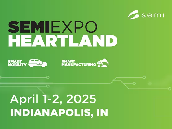
As the global semiconductor industry charges toward a projected $1 trillion market by 2030, regional innovation hubs are stepping into the spotlight. The inaugural SEMIEXPO Heartland—held April 1–2, 2025, at the Indiana Convention Center in Indianapolis—brought together key players from across the ecosystem to explore how advanced packaging, smart manufacturing, smart mobility, AI, and workforce development are fueling the semiconductor revolution.With a special focus on building self-reliance in the U.S. chip supply chain, the event highlighted efforts that are revitalizing the Midwest’s role as a key region driving innovation in the global semiconductor ecosystem. SEMIEXPO Heartland showcased leading-edge strategies and technologies from global giants and regional champions alike—underscoring the deep connections between government, academic, research, and industry leaders.Keynote HighlightsSK hynix: Accelerating the Future with Chiplets and Advanced PackagingDr. Woong Sun Lee, Senior Vice President at SK hynix, kicked off the event with a powerful vision for the future of semiconductor manufacturing. In response to skyrocketing demand fueled by AI, autonomous vehicles, and next-gen mobile applications, SK hynix is pursuing aggressive innovation through heterogeneous integration and chiplet-based design.Using 12-inch wafers, SK hynix’s chiplet strategy compresses product development timelines from 10-20 years to as little as 2-5 years. This leap in design efficiency enables faster time-to-market and greater performance optimization—crucial in an industry where speed and scale are paramount.A major component of this vision is the company’s investment in a state-of-the-art advanced packaging facility in Indiana. Targeting mass production by 2028, the new hub will not only expand SK hynix’s U.S. manufacturing footprint but also support national goals around workforce development and ecosystem growth. It’s a bold move that aligns the company’s R D leadership with America’s strategic reshoring efforts.Robert Bosch Semiconductor: Driving the Future with Silicon Carbide (SiC)Thorsten Scheer, Regional President Mobility Electronics and Plant Manager at Bosch Roseville, presented a deep dive into how Bosch is preparing for the electrified mobility era. Central to Bosch’s strategy is the adoption of silicon carbide (SiC) semiconductors, which are increasingly critical to electric vehicle powertrains.As vehicles become more connected and automated, Bosch projects more than 40 semiconductor chips per car by 2035. To meet this demand, Bosch is developing dual-channel trench MOSFET technology using SiC—a move that enhances power conversion efficiency and reduces heat, two of the biggest challenges in EV design.Bosch’s global expansion includes a new SiC wafer fab in Roseville, California, which is set to begin production in 2026. This facility is not only a technological investment but also a commitment to supply chain resilience, ensuring that the U.S. plays a central role in future automotive innovation.Polar Semiconductor: Reshoring Advanced Foundry CapabilitiesSurya Iyer, President and COO of Polar Semiconductor, shared the company’s mission to reinvigorate America’s semiconductor manufacturing capabilities. Headquartered in the Midwest, Polar is a rare U.S.-owned foundry playing a strategic role in reshoring production and building domestic capacity.Specializing in power semiconductors—including MOSFETs, IGBTs, and wide-bandgap (GaN) devices—Polar focuses on serving critical sectors such as automotive, aerospace and defense, and industrial applications. With advanced automation and a commitment to cost-efficient scale, the company is helping to bring more semiconductor innovation back to U.S. soil.Polar’s flexible business models and emphasis on workforce training position it as a linchpin in the nation’s efforts to build a more secure and agile semiconductor supply chain.Smart Manufacturing and Mobility SessionsUnlocking the Future with AI, Edge, and Digital TwinsThe opening session on April 1 showcased how AI and advanced simulation are transforming the semiconductor manufacturing process. NHanced Semiconductor introduced "Foundry 2.0," a platform delivering chiplet-based solutions tailored for low-volume, high-mix applications—highlighting flexibility and speed.Kulicke Soffa emphasized the use of AI, digital twins, and agentic automation in backend operations, helping to cut costs and boost efficiency. Humatics demonstrated its Milo microlocation system, addressing factory automation and labor challenges with precision positioning technologies.Meanwhile, Purdue University’s research in chip-package co-design and semiconductor education reflected the essential role of academia in building future-ready capabilities.AI, Edge, and Digital Twins in Backend ManufacturingThis session continued to explore the shift toward intelligent, connected manufacturing ecosystems. Allan Lewis of Nordson Electronics Solutions showcased AI-powered inspection systems that reduce downtime and improve yield.Jim Redman from ErgoTech Systems emphasized the importance of scalable, decentralized data platforms using low-code tools. Luis Rivera of Koh Young Technology introduced KSMART Server and CFX standards, enabling real-time optimization and machine-to-machine communication.Josh Mangahas from INFICON detailed how digital twins and AI/ML models are enhancing production scheduling and delivery timelines, while Mahesh Deshpande of Dassault Systèmes illustrated how virtual twins and XR-based tools are supporting agile packaging environments.The Convergence of AI, Robotics, and Digital TwinsSession 3 on April 2 featured cross-disciplinary insights from leaders at Arizona State University (ASU), Fraunhofer IZM, Teradyne, and Purdue. A common theme: AI, robotics, and digital twins are converging to redefine factory dynamics.Dr. Binil Starly (ASU) explained how reinforcement learning and MQTT protocols are enabling adaptive robotic inspections. Erik Jung (Fraunhofer IZM) highlighted how packaging and AI systems evolve in tandem to achieve tighter integration and higher performance.Teradyne’s Mat Najibnia focused on the ROI of robotic material handling systems, while Purdue’s Dr. Martin Jun shared a vision for democratized smart manufacturing—especially for small and medium-sized manufacturers (SMMs).Building Future-Ready Semiconductor EcosystemsThe final session underscored the importance of collaboration, resilience, and cybersecurity. Athinia discussed its work harmonizing raw material and fab data to improve manufacturing insights. IBM presented use cases combining digital twins and generative AI for yield improvement and predictive maintenance.Siemens focused on sustainability and decarbonization through digital twin platforms. The Florida Semiconductor Engine (FSE) illustrated how regional ecosystems can support leadership in packaging innovation and talent development.PEER Group spotlighted the Semiconductor Manufacturing Cybersecurity Consortium (SMCC), advocating for a standardized, collaborative approach to securing manufacturing infrastructure.Workforce Development and Regional ImpactA strong undercurrent throughout SEMIEXPO Heartland was the need for strategic workforce development. The event featured a Workforce Pavilion offering job seekers access to career coaching, resume guidance, and mentorship.Local universities and community colleges were well represented, as were federal and state workforce programs. These partnerships are crucial to ensuring a robust talent pipeline and equipping workers with the skills needed for a rapidly evolving industry.The presence of SK hynix, Polar, and other major players making sizable investments in the Midwest signaled not just a resurgence of regional manufacturing, but a renewed commitment to community growth, equitable opportunity, and long-term sustainability.A Midwest Moment with Global ImplicationsSEMIEXPO Heartland 2025 captured a pivotal moment in the evolution of the semiconductor industry. From chiplets and SiC to AI-driven smart factories and cyber-resilient ecosystems, the event highlighted how innovation, collaboration, and policy alignment are driving progress.As America looks to fortify its semiconductor future, the Midwest is emerging as a powerhouse of talent, technology, and tenacity. With support from industry, government, and academia, the region is well-positioned to lead the charge into a smarter, more secure, and more resilient semiconductor era.For questions about SEMI’s Smart Manufacturing initiative, contact Anshu Bahadur at [email protected]. Read more about SEMIEXPO Heartland in this press release: Inaugural SEMIEXPO Heartland Event Underscores Midwestern U.S. as a Global Hub for Smart Manufacturing and Smart Mobility.Anshu Bahadur is Sr. Program Manager, Technology Communities at SEMIRafael Tudela is Sr. Technical Marketing Manager at SEMI