downloadGroupGroupnoun_press release_995423_000000 copyGroupnoun_Feed_96767_000000Group 19noun_pictures_1817522_000000Member company iconResource item iconStore item iconGroup 19Group 19noun_Photo_2085192_000000 Copynoun_presentation_2096081_000000Group 19Group Copy 7noun_webinar_692730_000000Path
Skip to main content
Default Banner Image

IBM

Let’s celebrate! As of April/May 2020, Advanced Substrate News – or ASN for short, and now aka the SOI Consortium newsletter – has been bringing you news for 15 years. I hope you’ll forgive me if this post has a personal angle, as I have been the Editor-in-Chief since Day 1 back in 2005. One of the things I’ve learned over my career covering technology in general and SOI in particular is that “new” technologies are never really new. They don’t pop out fully formed like Venus Boticelli-style. They take years – decades, even. SOI is no exception. What is exceptional about SOI imho is that the ecosystem – from the substrate providers to the end-product designers – keeps finding new things to do with it. There have always been naysayers – and for a while it took on an quasi-fanatic ferocity. There were those who quipped that SOI was the technology of the future...and always would be. But as it turns out, SOI’s is, has been and will be the right technology at many right moments, and I don’t see any sign of that changing in the years to come. We Need a Newsletter! [caption id="attachment_32012" align="alignright" width="189"] My Design News piece on SOI from June 2000 - it changed my life![/caption] 
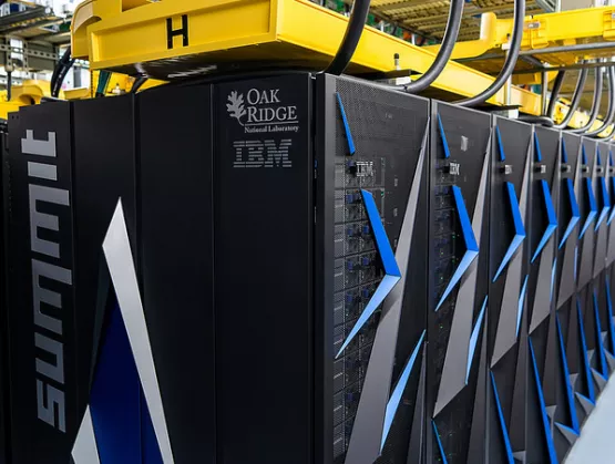
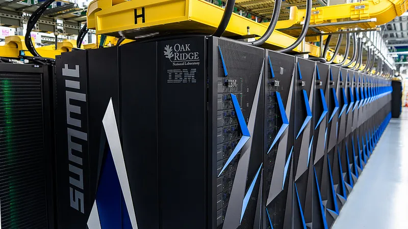
As so much in the SOI story, ASN began with Soitec. I first encountered Soitec when I was working as Contributing Editor in Europe for Semiconductor International in the mid 1990’s. It was a start-up of just a few people that made silicon-on-insulator aka SOI wafers. Most of us at the time had barely a notion of what that was all about, but they had an intriguing story to tell about higher performance and lower power. It so happened a few years later (circa 2000) I was also writing for another publication called Design News – not about chip design, but product design, for folks designing cars and consumer electronics and washing machines and such. I kept hearing a new requirement added to the product-design mantra of faster-smaller-cheaper: lower power. It seemed to me that these SOI wafers could go a long way in solving some of product designers’ challenges. I pitched a story to my editor and it wound up on the cover (those were the days some might remember when trade magazines were on paper…). The big players were IBM for digital (in a current-events aside, DKY that those big iron machines at the US national labs cranking on the solutions for the current pandemic use IBM FinFET-on-SOI chips? Just saying…), Philips (now NXP) for power/analog, and Soitec for wafers – and of course Honeywell for aerospace and the big electronics players in Japan for all sorts of things automotive and ultra-low power. Top management at Soitec read the piece and saw that I “got it”. They brought me on board as a consultant, writing early websites, PR, brochures and such. But also most importantly, they invited me “in” – I sat in on sales reviews and attended the big shin-digs they sponsored on the Riviera and in the Alps. The people I met there – and stayed in touch with – were many of the ones that drive the industry today. (Of course, that was then, this is now: I don’t have that insider status any more, but I’ve kept in touch with and often still rely on the expert advice of people I met during that heady time.) Anyway, one day at the end of 2004, the Soitec folks said to me, “We need a newsletter.” They asked me to come up with a concept they could pitch to the Board. Since Soitec was also doing GaN SiC at the time, I thought it should be called Advanced Substrate News – ASN for short. And we agreed it should involve the entire ecosystem: end users, equipment manufacturers, academics, suppliers of all sorts, and especially: chip designers. But it was not an easy pitch. Who’d want to read about SOI wafers, they asked? Wouldn't we run out of things to say after two or at most three editions? But the idea was a solid one: ASN could be a bully pulpit for the nascent SOI ecosystem. Happily it won the day. 
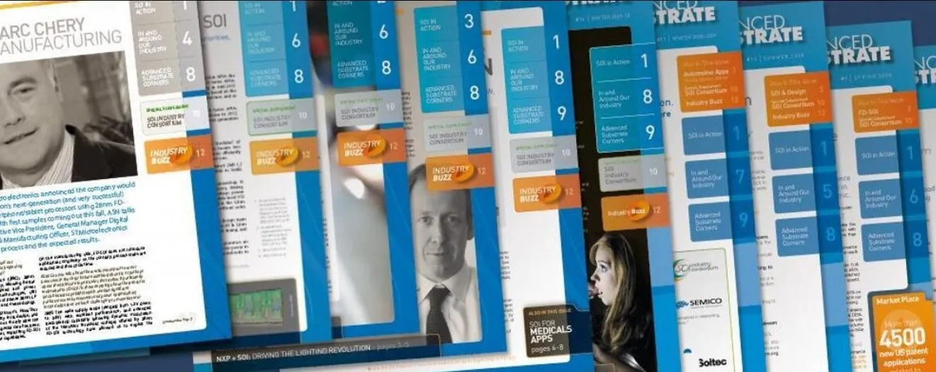
I was named Editor-in-Chief, and have held that title ever since. Our very first edition (we were a print quarterly then) had about a dozen articles on SOI, including automotive with Philips, ultra-low power FD-SOI with Oki for Casio’s G-Shock watches (oh yes – it goes back a long ways!), low-power (by a company that Arm then bought), high-performance, high-resistivity SOI wafers for RF…it was all there. And if you look at what we cover now, it’s still all there – albeit better than ever and growing fast. (I just listened to the most recent Soitec Q4'20 quarterly financial report audiocast – announcing that they’d just had their best quarter ever – largely driven by RF-SOI.) We Need a Consortium! In 2007, the SOI Consortium was created with 19 members (a dozen of whom are still members today). As ASN Editor-in-Chief, I was honored to be part of that effort, participating in the meetings where we hashed out what it was all about and what a consortium would do. It was a great opportunity to meet the movers and shakers across the industry, many of whom I’m still in touch with. 
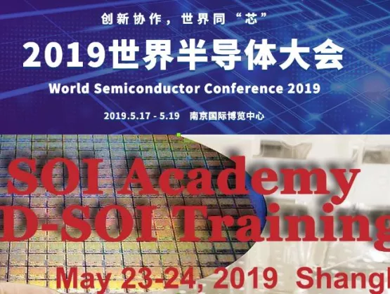
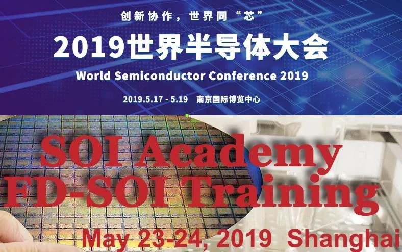
We published steadily, as the years, technologies and applications came and some went, but ASN readership continued to grow worldwide. Then in 2015, I got an email from the head of the Shanghai Academy of Sciences, which had recently spun off an SOI wafer maker called Simgui. He was (and is!) an ASN reader (though now he’s China’s Vice-Minister of Science Technology). Would I come to Shanghai and present some of the SOI-based applications ASN had been covering to his team there? They’d been working on SOI in parallel for many years, and were interested in where it was going in Europe and America. That was exciting! My first trip (of many, now) to China, it coincided with Semicon China 2015 and the announcement of the “Big Fund”. It was hall upon massive hall of stands immense and tiny, and the level of excitement was nothing short of amazing. (I was one of the only Western journalists there, and essentially broke the story in a piece I wrote for Consortium member Applied Materials’ customer magazine). That trip opened a lot of doors for me and ASN. As the SOI Consortium teamed up to with partners in China to host symposia there, we devoted more and more extensive coverage in ASN to those exciting events. [caption id="attachment_32041" align="alignright" width="328"] Here's some of our core players at the SOI Consortium: Executive Co-Directors Carlos Mazure (also of Soitec) and Jon Cheek (also of NXP) on the far left and right, respectively, Event Manager Iris Rith in the middle, me (Adele Hars) next on the right. We're joined here by Lucy Dai (2nd from left) of Simgui.[/caption] Eventually in 2016, ASN moved under the aegis of the SOI Consortium. We’re quite a jolly band that I have the privilege of working with. Granted at the time of this writing, the world is a difficult place, with so much uncertainty. But there are exciting times ahead with new products and technologies enabled by SOI, and you can be sure we’ll be covering them. RF-SOI will continue its juggernaut path in 5G mmWave. FD-SOI is steadily defining the new mainstream at the edge. The huge amounts of data the world is generating is driving photonics (which is all about SOI) to new heights. SOI for power (meaning high-voltage – think smart power) and imagers continues to grow. [caption id="attachment_32045" align="alignleft" width="99"] That's me - Adele Hars, ASN Editor-in-Chief - at the SOI Consortium's 2019 FD-SOI Symposium. (Photo courtesy VeriSilicon)[/caption] I’m honored to have brought you ASN for the last 15 years. Our archives are truly a treasure trove, and our mailing list of over 2500 really is an industry who's who. We’ve published well over a thousand (!) pieces in that time, most of which I’ve written with guidance from many an expert. However, we of course encourage our readers to pitch stories and/or submit SOI articles for publication consideration - so please, don't hesitate! I want to thank you all for your interest and your continued support. And thank you especially to all the SOI experts out there who so generously – and so patiently – share their time and enthusiasm with me and our readers. Stay safe! With warm regards, - Adele P.S. If you're not already on our emailing list and would like to join, just fill in the form at the bottom of this page. Thanks!
Read More
The SOI Consortium and member companies had a significant presence at two important events in China recently: the World Semiconductor Congress (WCS) in Nanjing and the SOI Academy, including an FD-SOI Training Day in Shanghai. Nanjing is especially known as a leading RF chip design hub in China, but WCS went well beyond RF. The three-day 2019 event was held at the Nanjing International Expo Center. It attracted over 30,000 visitors, 5000 of whom attended the various summit forums. Presenting at WCS '19 in Nanjing (clockwise from top left): Wayne Dai, CEO/Founder, VeriSilicon; Carlos Mazure, Executive Director, SOI Consortium; Giorgio Cesana, Director, STMicroelectronics; Christophe Tretz, Design Expert, SOI Consortium. (Photos courtesy: WCS)The SOI Consortium organized the SOI Forum, which was part of an afternoon Innovation Summit. Presentations were given by members of the SOI Consortium team, and by leaders from our membership, including Simgui, NXP, Incize, ST, IBM, Cadence and Xpeedic. Some of those presentations are now available from our website -- click here to get them.Earlier in the day, SOI Consortium member VeriSilicon participated in a morning session on AI and IoT Wireless Communications. They presented their low-power Bluetooth design platform for GlobalFoundries 22FDX, and CEO Wayne Dai moderated a lively round-table discussion.Following hard on the heels of the Nanjing event, the SOI Consortium team and members headed to Shanghai for the SOI Academy 2019, hosted for the second year in a row by member SIMIT (Shanghai Institute of Microsystem and IT under the Chinese Academy of Sciences). The two-day event attracted more than 250 professionals from more than 100 domestic and foreign IC companies and research institutes. Keynotes by SOI Consortium Executive Director Carlos Mazure, SITRI CEO Mark Ding and Jean-Eric Michallet, Head of the Microelectronics Components Department at Leti and bizdev director for the SOI Consortium focused on the SOI ecosystem. The SITRI and Leti talks also gave updates on their research and industrialization alliance. Further talks were given by leaders from Soitec, GlobalFoundries, VeriSilicon, IBM and Xpeedic. These addressed the growing FD-SOI ecosystem, applications in automotive electronics, 22 nm and 10 nm FD-SOI devices, advanced SOI substrate technology, China’s FD-SOI development, the FD-SOI manufacturing process, product design, EDA tools and all aspects of industry’s software and modeling value chain.Several speakers noted that more and more local Chinese customers are actively adopting FD-SOI for low-power, high-performance chips. SOI Academy, Shanghai, 2019, FD-SOI Training Day attendees.(Photo credit: SIMIT)The second day was devoted to hands-on professional training, given by experts from Leti using an actual PDK and punctuated by in-depth discussions. This helped the IC designers to fully understand the advantages and flexibility of FD-SOI in low-power logic, analog/mixed-signal and RF. All in all, “It was a great success,” concluded Jean-Eric MICHALLET, Head of the Microelectronics Components Department at Leti and bizdev director for the SOI Consortium. Plans for the next SOI Academy are already underway, with plans to extend the topics to include more on photonics, RF, power and MEMS.
Read More
Join us! In partnership with our members, the SOI Consortium is co-organizing and participating in two key SOI events coming up in China over the next few weeks. On May 18th, we’ve put together an SOI Forum at the World Semiconductor Congress (WCS) in Nanjing. And on May 23rd 24th, we’ve teamed up with our members SIMIT, Sitri and Leti for another in our series of SOI Academies, including an FD-SOI Training Day. (The last one this past winter was a terrific success – read about that here if you missed our coverage at the time.) QR code for WCS, Nanjing '19At WCS, the SOI Forum (sub-forum #8) is part of the afternoon Innovation Summit. We’ll cover the broader SOI ecosystem, including both RF-SOI and FD-SOI – from wafers to design through manufacturing. Presentations will be given by members of the SOI Consortium team, and by leaders from our membership, including Simgui, NXP, Incize, ST, IBM, Cadence and Xpeedic. Click here or scan the QR code for the full program and registration information. Also at WCS, SOI Consortium member VeriSilicon will be participating in a morning session on AI and IoT Wireless Communications (sub-forum #4). They’ll be giving a presentation on their low-power Bluetooth design platform for GlobalFoundries 22FDX, and their CEO Wayne Dai will be moderating a round-table discussion. You can get more information on that (in Chinese only, tho) here, or follow VeriSilicon on WeChat. QR code for SOI Academy and FD-SOI Training, Shanghaid 2019The SOI Academy in Shanghai is an opportunity for experienced designers to gain solid expertise in FD-SOI. The event begins in the afternoon of May 23rd with a series of informative plenary talks by members of the SOI Consortium team, and by experts from our members Leti, Soitec, VeriSilicon, GlobalFoundries and NXP. The FD-SOI Training starts the next morning, on May 24th.. This is a hands-on event lead by top experts from Leti. The morning is devoted to digital design in FD-SOI, and the afternoon to RF design (including for 5G) in FD-SOI. Attendees will get a comprehensive understanding of design techniques for low-power chips leveraging the multiple benefits and flexibility of FD-SOI technology. Get more information here, or from the WeChat QR code.We've got a busy schedule! To keep up to date with where we and our members will be promoting the SOI ecosystem, be sure to check our Events page regularly.
Read More
The CPUs in Summit, the world's new fastest supercomputer are built on 14nm FinFET-on-SOI technology. Yes, those IBM Power9 CPUs are fabbed by GlobalFoundries (you'll also find them in the z14, the most recent in IBM's z-series of servers – a series that's been on various iterations of SOI since its launch in 2003, btw). Summit's at the U.S. Department of Energy’s Oak Ridge National Laboratory (ORNL) in Tennessee, USA. It is now the top US supercomputer, and it's for science. The IBM-built Summit currently claims the spot in the Top500 as the world's smartest and most powerful supercomputer. “It is capable of performing 200 quadrillion calculations per second — or 200 petaflops — making it the fastest in the world,” says IBM's Dr. John E. Kelly, III, SVP, Cognitive Solutions and IBM Research. “But this system has never been just about speed. Summit is also optimized for AI in a data-intense world. We designed a whole new heterogeneous architecture that integrates the robust data analysis of powerful IBM Power CPUs with the deep learning capabilities of GPUs. The result is unparalleled performance on critical new applications.” And if that's not impressive enough for you, it's also #5 on the Green500 list for the world's most energy-efficient computers, posting Power Efficiency (GFlops/watts) of 13.889. [caption id="attachment_11940" align="alignright" width="300"] Summit supercomputer nodes: The IBM-built Summit supercomputer is the world's smartest and most powerful AI machine. It consists of 4,600 individual nodes. Each node contains two 22-core 3.07GHz IBM POWER9 CPUs, which are built on GlobalFoundries' 14nm HP FinFET-on-SOI technology, as well as six NVIDIA Telsa GPUs. (Photo Credit: ORNL).[/caption] As GF noted when they announced the technology in the fall of 2017 (read the GF press release here), their 14HP is the industry’s only technology to integrate a FinFET transistor architecture on SOI. Featuring a 17-layer metal stack and more than eight billion transistors per chip, the technology leverages embedded DRAM and other innovative features to deliver higher performance, reduced energy, and better area scaling over previous generations to address a wide range of deep computing workloads. These technologies have long, deep histories (and were developed in close collaboration with SOI wafer leader Soitec). Here at ASN we have a fabulous archive of pieces contributed by IBM explaining the genesis of the technology – they're great reads and still entirely pertinent: FinFET on SOI: Potential Becomes Reality (by T.B. (Terry) Hook et al, 2013) – this presents the key technical data. IBM: Why Fin-on-Oxide (FOx/SOI) Is Well-Positioned to Deliver Optimal FinFET Value (by Terry Hook, 2012) – this great piece busts myths and clearly explains why FinFETs on SOI deliver top performance. IBM: FinFET Isolation Considerations and Ramifications – Bulk vs. SOI (by Terry Hook, 2013) – explains why and how SOI increases operating voltage range, simplifies processing, reduces variation, lowers soft error rate, and enables higher circuit density. Embedded Memories in SOI – (by Subramanian S. Iyer, 2006) explains the importance of SOI in the memory part of the chip design equation. [caption id="attachment_11939" align="alignleft" width="300"] The IBM POWER9 processor delivers unprecedented speeds for deep learning and AI workloads. IBM Engineer, Stefanie Chiras tests the IBM Power System server in Austin, Texas. (Photo Credit: Jack Plunkett/Feature Photo Service for IBM).[/caption] As ORNL noted in its press release (you can read it here), the first projects will apply machine learning and AI to astrophysics, materials science, cancer research and systems biology. BTW, Summit also has a slightly smaller sister machine called Sierra, going in at the Lawrence Livermore National Laboratory (part of the Department of Energy's National Nuclear Security Administration). With 4,320 nodes (each also containing two 22-core 3.07GHz IBM POWER9 CPUs, which are built on GlobalFoundries' 14nm HP FinFET-on-SOI technology, but just four NVIDIA Telsa GPUs), Sierra's claimed the #3 spot on the June 2018 Top500 list of the world's most powerful supercomputers. And the Power 9 is now finding it's way into major data centers – like Google's (read about that here). There have been some good pieces in the press about it, including in Forbes and The Motley Fool. So yes, clearly there are exciting markets for FinFETs on SOI!
Read More