downloadGroupGroupnoun_press release_995423_000000 copyGroupnoun_Feed_96767_000000Group 19noun_pictures_1817522_000000Member company iconResource item iconStore item iconGroup 19Group 19noun_Photo_2085192_000000 Copynoun_presentation_2096081_000000Group 19Group Copy 7noun_webinar_692730_000000Path
Skip to main content
Default Banner Image

high-performance

The CPUs in Summit, the world's new fastest supercomputer are built on 14nm FinFET-on-SOI technology. Yes, those IBM Power9 CPUs are fabbed by GlobalFoundries (you'll also find them in the z14, the most recent in IBM's z-series of servers – a series that's been on various iterations of SOI since its launch in 2003, btw). Summit's at the U.S. Department of Energy’s Oak Ridge National Laboratory (ORNL) in Tennessee, USA. It is now the top US supercomputer, and it's for science. The IBM-built Summit currently claims the spot in the Top500 as the world's smartest and most powerful supercomputer. “It is capable of performing 200 quadrillion calculations per second — or 200 petaflops — making it the fastest in the world,” says IBM's Dr. John E. Kelly, III, SVP, Cognitive Solutions and IBM Research. “But this system has never been just about speed. Summit is also optimized for AI in a data-intense world. We designed a whole new heterogeneous architecture that integrates the robust data analysis of powerful IBM Power CPUs with the deep learning capabilities of GPUs. The result is unparalleled performance on critical new applications.” And if that's not impressive enough for you, it's also #5 on the Green500 list for the world's most energy-efficient computers, posting Power Efficiency (GFlops/watts) of 13.889. 
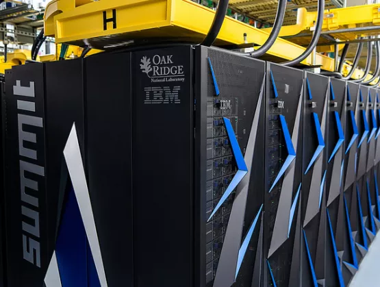
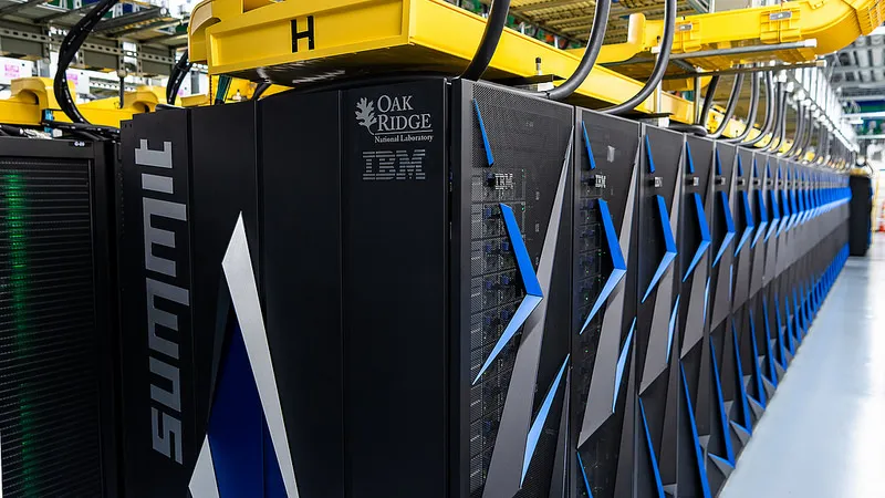
[caption id="attachment_11940" align="alignright" width="300"] Summit supercomputer nodes: The IBM-built Summit supercomputer is the world's smartest and most powerful AI machine. It consists of 4,600 individual nodes. Each node contains two 22-core 3.07GHz IBM POWER9 CPUs, which are built on GlobalFoundries' 14nm HP FinFET-on-SOI technology, as well as six NVIDIA Telsa GPUs. (Photo Credit: ORNL).[/caption] As GF noted when they announced the technology in the fall of 2017 (read the GF press release here), their 14HP is the industry’s only technology to integrate a FinFET transistor architecture on SOI. Featuring a 17-layer metal stack and more than eight billion transistors per chip, the technology leverages embedded DRAM and other innovative features to deliver higher performance, reduced energy, and better area scaling over previous generations to address a wide range of deep computing workloads. These technologies have long, deep histories (and were developed in close collaboration with SOI wafer leader Soitec). Here at ASN we have a fabulous archive of pieces contributed by IBM explaining the genesis of the technology – they're great reads and still entirely pertinent: FinFET on SOI: Potential Becomes Reality (by T.B. (Terry) Hook et al, 2013) – this presents the key technical data. IBM: Why Fin-on-Oxide (FOx/SOI) Is Well-Positioned to Deliver Optimal FinFET Value (by Terry Hook, 2012) – this great piece busts myths and clearly explains why FinFETs on SOI deliver top performance. IBM: FinFET Isolation Considerations and Ramifications – Bulk vs. SOI (by Terry Hook, 2013) – explains why and how SOI increases operating voltage range, simplifies processing, reduces variation, lowers soft error rate, and enables higher circuit density. Embedded Memories in SOI – (by Subramanian S. Iyer, 2006) explains the importance of SOI in the memory part of the chip design equation. [caption id="attachment_11939" align="alignleft" width="300"] The IBM POWER9 processor delivers unprecedented speeds for deep learning and AI workloads. IBM Engineer, Stefanie Chiras tests the IBM Power System server in Austin, Texas. (Photo Credit: Jack Plunkett/Feature Photo Service for IBM).[/caption] As ORNL noted in its press release (you can read it here), the first projects will apply machine learning and AI to astrophysics, materials science, cancer research and systems biology. BTW, Summit also has a slightly smaller sister machine called Sierra, going in at the Lawrence Livermore National Laboratory (part of the Department of Energy's National Nuclear Security Administration). With 4,320 nodes (each also containing two 22-core 3.07GHz IBM POWER9 CPUs, which are built on GlobalFoundries' 14nm HP FinFET-on-SOI technology, but just four NVIDIA Telsa GPUs), Sierra's claimed the #3 spot on the June 2018 Top500 list of the world's most powerful supercomputers. And the Power 9 is now finding it's way into major data centers – like Google's (read about that here). There have been some good pieces in the press about it, including in Forbes and The Motley Fool. So yes, clearly there are exciting markets for FinFETs on SOI!
Read More
By: Tamer Ragheb,Digital Design Methodology Technical Manager at GlobalFoundries and Josefina Hobbs, Senior Manager of Strategic Alliances, Synopsys It’s clear that getting an optimal balance of power and performance at the right cost is foremost in the minds of designers today. Designers who want either high performance or ultra low-power, or ideally both, have a choice to make when it comes to migrating to next generation nodes. For applications that push the envelope in performance, FinFET would be the optimal solution. For applications that require ultra low-power and more RF integration, FD-SOI is the right solution. The two technologies have different value propositions that need to be considered while designing for applications ranging from high-performance computing and server to high-end mobile and Internet of Things (IoT). GlobalFoundries 22FDX is the industry’s very first 22nm FD-SOI platform. The 22FDX technology is specifically designed to meet the ultra low-power requirements of the next generation of connected devices. The big advantage of this platform is its ability to provide software control at the transistor level through flexible body-biasing (Fig. 1). The ability to provide real-time trade-offs between power and performance via software-controlled body-biasing of the transistor creates new options for the designer. For example, imagine designing a processor for a Smartwatch that could match its power-performance tradeoff to your typical use and modify its performance based on how you’re using it that day. [caption id="attachment_9473" align="alignleft" width="610"] Figure 1: Benefits of 22FDX body-biasing[/caption] The full impact of the body bias capability of 22FDX becomes clear when compared to incumbent high-performance process technologies (Fig. 2). 22FDX compared to a 28nm high K metal gate (HKMG) technology can provide up to 50% less power at the same frequency, or 40% faster performance at the same total power than 28HKMG. In addition, 22FDX can be further optimized with forward body bias, shown on the blue curve, to further reduce the power or to further boost the speed in a turbo operation mode. [caption id="attachment_9474" align="alignleft" width="610"] Figure 2: 22FDX Body Bias Optimizes Performance and Power[/caption] In addition to the body bias, 22FDX offers capabilities for design flexibility and intelligent control that are not available in other technologies. These include: Improved electrostatic control of the transistor acts as a performance booster and enables lower VDD (i.e., lower power consumption) while reaching significant performance Low variability and body-biasing capability that can achieve 0.4 volt operation Complete RF enablement with ‘knobs’ to reduce RF power by up to 50 percent Manufacturing success is highly sensitive to specific physical design features, with advanced nodes requiring more complex design rules and more attention to manufacturability issues on the part of designers. However, there are essentially no additional manufacturing requirements to design in 22FDX beyond what is required for 28nm designs. There are four application optimized extensions available with 22FDX (Fig. 3). These are: 22FDX ULP- an ultra low-power extension that provides logic libraries and memory compilers that are optimized for 0.4 volt operation. 22 FDX ULL- an ultra low-leakage extension that brings in an expanded device suite capable of achieving one pico-amp per micron leakage. 22 FDX UHP- an ultra high-performance extension that leverages the overdrive capabilities and body-biasing features to maximize the performance of technologies in a turbo or a burst mode. It has high performance libraries and high speed interfaces and BEOL stacks optimized for competing architectures or applications. 22 FDX RFA- an RF and analog extension that brings in full characterization and enablement for RF applications, including optimized RF layouts and P cells, BEOL passives, and IP for Bluetooth LE and WIFI applications. [caption id="attachment_9475" align="alignleft" width="610"] Figure 3: 22FDX Platform and Extensions[/caption] GlobalFoundries reference flow for 22FDX has been optimized to support forward and reverse body bias (FBB/RBB), which provides the design flexibility to optimize the performance/power trade-offs. The reference flow supports implant-aware and continuous diffusion-aware placement, tap insertion and body bias network connectivity according to high voltage rules, double-patterning aware parasitic extraction (PEX), and design for manufacturing (DFM). This provides designers with the flexibility to manage power, performance and leakage targets for the next-generation chips used in mainstream mobile, IoT and networking applications. GlobalFoundries has been collaborating with Synopsys to enable and qualify their tools for the 22FDX Reference Flow. The recent qualification of Synopsys’ Galaxy™ Design Platform for the current version ofGlobalFoundries’ 22FDX technology allows the designer to manage power, performance and leakage and achieve optimal energy efficiency and cost effectiveness. Synopsys’ Galaxy Design Platform supports body biasing techniques throughout the design flow, including both forward and reverse body bias, enabling power/performance trade-offs to be made dynamically and delivering up to 50% power reduction. Key tools and features of the Galaxy Design Platform in the 22FDX reference flow include: Design Compiler® Graphical synthesis with IEEE 1801 (UPF) driven bias-aware multi-corner multi-mode (MCMM) optimization Formality® formal verification with bias-aware equivalence checking IC Compiler™ and IC Compiler II™ layout with physical implementation support for non-uniform library floorplanning, implant-aware placement, multi-rail routing, and advanced power mesh creation StarRC™ parasitic extraction for multi-rail signoff with support for multi-valued standard parasitic exchange format (SPEF) PrimeTime® timing analysis and signoff including distributed multi-scenario analysis (DMSA) static timing and noise analysis, using AOCV and POCV technology IC Validator In-Design physical verification The 22FDX technology leverages existing design tools such as the Galaxy Design Platform, manufacturing infrastructure and the broader design ecosystem. This speeds time to market and enables the creation of differentiated products.
Read More