downloadGroupGroupnoun_press release_995423_000000 copyGroupnoun_Feed_96767_000000Group 19noun_pictures_1817522_000000Member company iconResource item iconStore item iconGroup 19Group 19noun_Photo_2085192_000000 Copynoun_presentation_2096081_000000Group 19Group Copy 7noun_webinar_692730_000000Path
Skip to main content
Default Banner Image

mobile

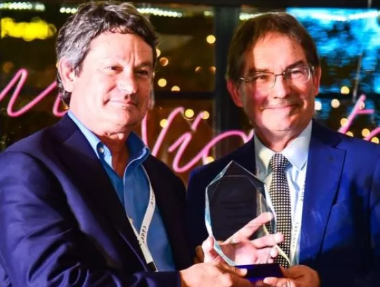
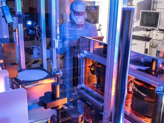
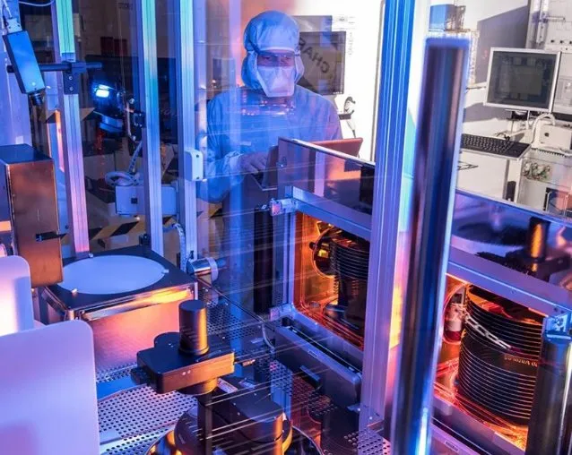
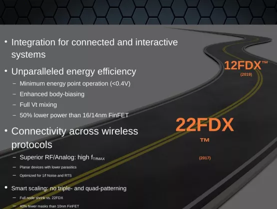
With increasing demand for personalized smart devices, the MEMS and sensor market is undergoing rapid transformation. MEMS sensors are the backbone of smart wearable devices, seamlessly integrating multiple functions to monitor and simplify our day-to-day activities. As applications in healthcare, environmental tracking, and AR/VR expand, the need for ultra-compact, energy-efficient, and intelligent sensors is more critical than ever.In an exclusive conversation with SEMI, Stefan Finkbeiner, CEO of Bosch Sensortec, shared his perspective on the dynamic landscape of MEMS sensor technology. From Bosch’s evolution to a solutions provider with a focus on sustainability and market-driven innovations, Finkbeiner offered a deep dive into how Bosch Sensortec is positioning itself at the forefront of the industry. “We have to think in terms of the end application and determine what the right hardware and software configuration should be in order to provide solutions with the greatest benefit and flexibility.”Further insights into the future of MEMS and sensor technology will be shared by Finkbeiner during his keynote at the SEMI MEMS Imaging Sensors Summit on November 14, 2024, in Munich, Germany. Registration is still open.SEMI: Welcome, Stefan, and thank you for sharing your insights on advanced sensor technologies. Let’s start with a personal question: What motivates and inspires you about working in sensor technology?Finkbeiner: Sensor technology is very diverse and has significant impacts on consumers. We take pride in prioritizing consumers’ needs and benefits. True to the Bosch motto, “Invented for life,” we are committed to making life better, easier and healthier. This is demonstrated in our sensing solutions, which provide valuable data for fitness tracking in smartwatches, enhance the audio experience in hearables, and enable real-time monitoring of air quality to help individuals make informed decisions for a healthier environment. I am fascinated by technology advancements that are enabling the scaling of sensors—and the processing power and intelligence packed into these increasingly compact devices. For instance, our latest acceleration sensors for hearables are the smallest in the world and are nearly invisible at just 1.2 x 0.8 x 0.55 mm³.We leverage innovative wafer level chip scale packaging (WLCSP) to achieve this reduced form factor. These compact, feature-rich, high-performance accelerometers are easier to integrate in the latest generation consumer products where size and functionality are critical requirements.SEMI: How has Bosch Sensortec’s approach evolved over the years and what is the company’s primary focus today? Finkbeiner: We began our success story a few years ago as a hardware supplier, with one of our first applications being the 'Portrait-Landscape' function in smartphones. Over time, we’ve evolved into one of the leading providers of MEMS sensors.Today, we no longer see ourselves purely as a sensor manufacturer, but as a technology solutions provider. Our focus has shifted to think in terms of the end application and determine what the right hardware and software configuration should be to provide solutions with the greatest benefit and flexibility.Achieving this requires significant software and artificial intelligence (AI) development. In essence, we are optimizing software through self-learning models. Hardware remains essential for optimizing power consumption, with most sensors integrating a controller alongside the ASIC to enable seamless software integration.This unique software and hardware configuration unlocks exciting possibilities and broadens our market reach. We see significant growth in head-mounted devices, and we are actively working on related acoustics solutions.SEMI: Looking ahead, what trends do you anticipate will have the most significant impact on the MEMS sensors market?Finkbeiner: We see several trends that will significantly impact the MEMS sensor market. First, there is growing demand for personal health monitoring in consumer and mobile electronics. Wearable devices, in particular, are becoming essential tools for individuals to track their health and fitness status. This trend requires MEMS sensors to become even more accurate, with solutions that include sophisticated software algorithms to ensure reliability, accuracy, and reproducibility. As a result, AI and machine learning (ML) technologies will play a crucial role in enhancing sensor performance.A second important trend is the continued miniaturization of MEMS sensors. To meet customer demands, sensors must integrate more functionality, including edge-processing capabilities. For example, what once may have been a simple accelerometer with a step-counting algorithm is now evolving into a 6-axis Inertial Measurement Unit (IMU) with an integrated microcontroller and advanced AI/ML software. A great example of this is in True Wireless Stereo (TWS) earphones, where the IMU not only tracks steps but also enables complex tasks like dead reckoning and supports 3D audio—all within the tight constraints of a small TWS earbud housing. Low power consumption, as always, is a critical factor for these mobile devices to meet CE (Conformité Européenne) standards.Finally, we believe that smart glasses, augmented reality (AR) and virtual reality (VR) devices are poised to become the “next big thing.” These devices require advanced image projection optics that offer excellent optical quality, low weight, and ease of use to ensure consumer adoption. We believe our MEMS-based LBS (Laser Beam Scanning) solution is ideal for these applications. Additionally, the successful adoption of smart glasses hinges on high-performance MEMS sensors that are compact, accurate, and power-efficient—critical requirements for all-day wearability and functionality.These trends underscore the need for MEMS technology to evolve, integrating greater functionality, precision, and efficiency to meet the demands of next-generation consumer devices.SEMI: What are some of the biggest challenges facing the MEMS sensors industry today, and how can companies overcome them?Finkbeiner: One key challenge is that the smartphone market—arguably the most attractive market for a variety of MEMS and MOEMS sensors—has become more or less saturated. To stay competitive, MEMS companies must innovate existing products while also developing new, differentiated sensors and actuators for next-generation mobile products.SEMI: How is Bosch Sensortec supporting sustainability initiatives?Finkbeiner: We are helping to mitigate climate change with our low carbon footprint solutions.Up to 20% of annual global carbon emissions are caused by forest fires. This is equivalent to carbon dioxide emitted by all the vehicles driven worldwide. Our sensors can detect forest fires before they develop into wildfires by measuring various gases such as carbon monoxide and hydrogen. In parallel, we are working with our production partners to reduce our carbon footprint over the coming years, while also replacing or minimizing the use of environmentally hazardous chemicals, such as PFAS.SEMI: What are you most excited about for the MEMS Imaging Sensors Summit, and how do you think it will impact the European semiconductor industry?Finkbeiner: The European semiconductor industry has deep expertise in MEMS and sensor technologies, positioning it to make a significant impact in markets such as consumer health, optical sensing, and AR displays. By continuing to focus on sustainable solutions, we can drive even greater impact for the broader industry and secure Europe’s leadership in these growth sectors.I look forward to collaborating with industry peers at the Summit to define next steps needed to advance Europe’s leadership. The MEMS Summit is an invaluable opportunity to collaborate and drive progress, and I warmly invite my colleagues to join us in shaping the future of the European semiconductor industry.Dr. Stefan Finkbeiner Dr. Stefan Finkbeiner has been CEO and General Manager at Bosch Sensortec GmbH since 2012. He was born in 1966 in Freudenstadt, Germany. Stefan Finkbeiner held various senior positions at Bosch including Director of Sensor Marketing, Director of Corporate Research in microsystems technology, and Vice President of Sensor Engineering. He looks back on almost 30 years in semiconductor industry working in different positions related to sensor research, development, manufacturing, and marketing. Due to his wide experience in semiconductor and sensor industry, Stefan Finkbeiner is a recognized guest in panel discussions and as keynote speaker. SEMI ContactSitong He / Communications Manager, SEMI EuropeEmail: [email protected]: +49 151 5546 2638
Read More
The SOI Industry Consortium awarded two luminaries of the semiconductor industry for pioneering advances in RF-SOI, a technology now found in all cellphones. Jim Cable (shown on the left in the photo above), Chairman and CTO of pSemi, a Murata Company, and Herb Huang, CEO and GM of Ninbo Semiconductor received the awards during a gala following the SOI Consortium's 2019 RF-SOI Workshop in Shanghai. "Thanks in large part to the innovation, dedication and perseverance of men like Jim Cable and Herb Huang, RF technology based on SOI is now ubiquitous," said Carlos Mazure (on the right in the photo), Chairman and Executive Director of the SOI Consortium. "Jim Cable drove the development of SOI and RF switches that are now in every cellphone, and Herb Huang has been a key contributor to SOI technology and a champion of the SOI foundry ecosystem in China. We are happy and honored to recognize the contributions they have made to advancing RF-SOI globally." Jim Cable joined pSemi (formerly Peregrine Semiconductor) in 1996 and held technical leadership roles before serving as CEO from 2002 to 2017. An early pioneer of SOI technology, Cable believed SOI would ultimately replace other technologies in the RF front end, and he pushed his team to innovate. Cable is a co-inventor on more than 70 semiconductor and technology patents, including breakthroughs in SOI-based processes for CMOS RF switch linearity and integration that are used by all smartphones today, and will become even more mission-critical in 5G and millimeter-wave markets. He received his B.S. in physics from UC Riverside and his master's degree and Ph.D. in electrical engineering from UCLA. Herb Huang is CEO of Ningbo Semiconductor International Corporation (NSI), which is based in Ningbo, China. A driver of the RF-SOI ecosystem in China, he spent much of his career at SMIC, the largest semiconductor foundry company in mainland China. In 2016, SMIC created NSI as a joint venture subsidiary with China IC Investment Fund, Ningbo Economic Development Zone Industrial Investment Company, Ltd. and other IC investment funds. Under Huang's leadership, NSI optimized the process and model of a 0.13um RF-SOI technology platform transferred from SMIC. Now in mass production, the RF-SOI technology platform supports customers in IC design and product development for new generations of radio communications. Huang holds both a Ph.D in Materials Science and Engineering and an MBA from the University of Minnesota.
Read More
“GlobalFoundries, TowerJazz, TSMC and UMC are expanding or bringing up RF SOI processes in 300mm fabs in an apparent race to garner the first wave of RF business for 5G, the next-generation wireless standard,” writes Mark Lapedus of Semiconductor Engineering. His recent piece, RF-SOI Wars Begin, explains why demand across the supply chain is currently tight. Rest assured, the supply situation is being addressed fast. By next year, 300mm-based RF-SOI manufacturing (vs. 200mm) will increase from 5% to 20%. But with insatiable end-user demand for greater throughput, overall RF-SOI device demand is increasing in the double-digit range, so 200mm-based manufacturing is also expanding fast. [caption id="attachment_11905" align="alignleft" width="300"] The front-end modules in all smartphones are built on Soitec's RF-SOI wafer technology. The most advanced, for LTE/LTE-A, are built on Soitec's RFeSI-SOI wafers, which have four layers to meet the demands of devices with high linearity requirements. (Courtesy: Soitec)[/caption] SOI wafer manufacturer Soitec has 70% of the RF-SOI wafer market share. The other RF-SOI wafer manufacturers – Shin-Etsu, GlobalWafers and Simgui – all use Soitec's RF-SOI wafer manufacturing technology. This is an excellent, comprehensive piece, that clearly explains the complexities of the markets, the devices, the manufacturing and the supply chain. It's a highly recommended read. BTW, the SOI Consortium is organizing a 4G/5G SOI supply chain workshop during Semicon West (July '18). Sign up or get more information on that under the Events tab here on the consortium website. Of course, here at ASN, we've been covering RF-SOI for over a decade. You can use our RF-SOI tag to access most of the pieces we've done over the years.
Read More
12nm FD-SOI has now officially joined the GlobalFoundries’ roadmap, targeting intelligent, connected systems and beating 14/16nm FinFET on performance, power consumption (by 50%!) and cost (see press release here). Customer product tape-outs are expected to begin in the first half of 2019. GloFo also announced FDXcelerator™, an ecosystem designed to give 22FDX™ SoC design a boost and reduce time-to-market for its customers (press release here). [caption id="attachment_9874" align="aligncenter" width="610"] (Courtesy: GlobalFoundries and SOI Consortium Shanghai FD-SOI Forum 2016)[/caption] The news turned heads worldwide (hundreds of publications immediately picked up the news) – and especially in China. "We are excited about the GlobalFoundries 12FDX offering and the value it can provide to customers in China," said Dr. Xi Wang, Director General, Academician of Chinese Academy of Sciences, Shanghai Institute of Microsystem and Information Technology. “Extending the FD-SOI roadmap will enable customers in markets such as mobile, IoT, and automotive to leverage the power efficiency and performance benefits of the FDX technologies to create competitive products." Wayne Dai, CEO of VeriSilicon (headquartered in Shanghai but designing for the world’s biggest names in the chip biz), added, “We look forward to extending our collaboration with GlobalFoundries on their 12FDX offering and providing high-quality, low-power and cost-effective solutions to our customers for the China market. The unique benefits of FD-SOI technologies enable us to differentiate in the automotive, IoT, mobility, and consumer market segments.” The ultra-thin FD-SOI wafers are where it all starts, and they’re ready to go in high volume, says Paul Boudre, CEO of SOI wafer leader Soitec. “We are very pleased to see a strong momentum and a very solid adoption from fabless customers in 22FDX offering,” he adds. “Now this new 12FDX offering will further expand FD-SOI market adoption. This is an amazing opportunity for our industry just in time to support a big wave of new mobile and connected applications.” All About 12GloFo’s 12FDXTM platform, which builds on the success of its 22FDXTM offering, is designed to enable the intelligent systems of tomorrow across a range of applications, from mobile computing and 5G connectivity to artificial intelligence and autonomous vehicles. Increased integration of intelligent components including wireless (RF) connectivity, non-volatile memory, and power management—all while driving ultra-low power consumption—are key 12FDX selling points that FinFETs can’t touch. The technology also provides the industry’s widest range of dynamic voltage scaling and unmatched design flexibility via software-controlled transistors—capable of delivering peak performance when and where it is needed, while balancing static and dynamic power for the ultimate in energy efficiency. [caption id="attachment_9873" align="aligncenter" width="610"] (Courtesy: GlobalFoundries and SOI Consortium Shanghai FD-SOI Forum 2016)[/caption] “Some applications require the unsurpassed performance of FinFET transistors, but the vast majority of connected devices need high levels of integration and more flexibility for performance and power consumption, at costs FinFET cannot achieve,” said GLOBALFOUNDRIES CEO Sanjay Jha. “Our 22FDX and 12FDX technologies fill a gap in the industry’s roadmap by providing an alternative path for the next generation of connected intelligent systems. And with our FDX platforms, the cost of design is significantly lower, reopening the door for advanced node migration and spurring increased innovation across the ecosystem.” Kudos came in from G. Dan Hutcheson, CEO of VLSI Research, IBS CEO Handel Jones, Linley Group Founder Linley Gwennap, Dasaradha Gude, CEO of IP/design specialists INVECAS, Leti CEO Marie Semeria and NXP VP Ron Martino (they’ve already started on 28nm FD-SOI for their i.MX line – read his superb explanations in ASN here). 22 Design Plug ‘n PlaySimultaneously to the 12FDX announcement, GloFo announced the FDXcelerator Partner Program. It creates an open framework under which selected Partners can integrate their products or services into a validated, plug and play catalog of design solutions. This level of integration allows customers to create high performance designs while minimizing development costs through access to a broad set of quality offerings, specific to 22FDX technology. The Partner ecosystem positions members and customers to take advantage of the broad adoption and accelerating growth of the FDX market.Initial partners of the FDXcelerator Partner Program are: Synopsys (EDA), Cadence (EDA), INVECAS (IP and Design Solutions), VeriSilicon (ASIC), CEA Leti (services), Dreamchip (reference solutions) and Encore Semi (services). These companies have already initiated work to deliver advanced 22FDX SoC solutions and services. Initial FDXcelerator Partners have committed a set of key offerings to the program, including: tools (EDA) that complement industry leading design flows by adding specific modules to easily leverage FDSOI body-bias differentiated features, a comprehensive library of design elements (IP), including foundation IP, interfaces and complex IP to enable foundry customers to start their designs from validated IP elements, platforms (ASIC), which allow a customer to build a complete ASIC offering on 22FDX, reference solutions (reference designs, system IP), whereby the Partner brings system level expertise in Emerging application areas, enabling customers to speed-up time to market, resources (design consultation, services), whereby Partners have trained dedicated resources to support 22FDX technology; and product packaging and test (OSAT) solutions. Additional FDXcelerator members will be announced in the following months.
Read More