downloadGroupGroupnoun_press release_995423_000000 copyGroupnoun_Feed_96767_000000Group 19noun_pictures_1817522_000000Member company iconResource item iconStore item iconGroup 19Group 19noun_Photo_2085192_000000 Copynoun_presentation_2096081_000000Group 19Group Copy 7noun_webinar_692730_000000Path
Skip to main content
Default Banner Image

EDA

In the span of a few short months earlier this year, Mentor Graphics became Siemens EDA and introduced a suite of integrated hardware-assisted verification tools, the first product launch under the new Siemens EDA brand. Jean-Marie Brunet, senior director of marketing, product management and product engineering at Siemens EDA, orchestrated the launch and connected with me for a discussion about the chip design verification space. As he pointed out, verification and validation of systems is a fast-growing and important market segment to the electronic system design ecosystem. Smith: What trends do you see in chip design? What is driving these trends? Brunet: Chip verification costs continue to grow faster than design costs because of factors such as increasing design complexity, rising computing power, surging I/O traffic activity, increasing energy consumption and the widespread use of peripherals. These dynamics are being driven by new data center networking, communications/5G, autonomous driving, artificial intelligence (AI) and machine learning (ML), and storage applications. These trends also indicate the need for more powerful verification tools and expanded verification objectives that include power and performance analysis. Hardware-assisted verification tools are perfect for meeting these demands. Smith: Chip design verification consumes the most time in a project cycle. Why is this so? Brunet: The verification of designs reaching multi-billion gates and supported by voluminous software stacks is fraught with challenges. To exhaustively check every possible state in a billion-gate design with simulation alone would require up to trillions of verification cycles. That’s why hardware-assisted verification is one of the fastest-growing technologies in EDA. Given the complexity of today’s SoC design, it’s no surprise that verification is the largest undertaking in the entire project design cycle, consuming more than 50% of it. It also has the greatest impact on quality, cost and schedule because it prevents designs from failing at first silicon. While a respin of a large design taped out at a node below 10 nanometers could cost more than $10 million, delaying delivery of a new product for a few months in a highly competitive market may cost hundreds of millions of dollars. Smith: What other challenges do engineers face trying to verify a chip design will work as intended? Brunet: Verifying an SoC design is a massive undertaking and, in parallel, verification teams are trying to streamline and optimize verification cycles. SoC design groups are tasked with completing full system-level verification prior to creating production masks by thoroughly vetting all hardware blocks, interactions between those blocks, and the software developed for the end application before the chip is built. To alleviate this enormous pressure, they are starting to adopt a shift-left methodology for early functional verification as soon as individual blocks of a SoC design become available. It helps jump-start embedded software validation before full system validation is completed to save time and allow engineers to work in parallel, not serially. While it is an effective approach, it creates the need for a complete and integrated suite of hardware-assisted verification tools to verify and validate a design’s hardware and software components. Smith: How do you define hardware-assisted verification and how does it help solve these challenges? Brunet: A typical definition of hardware-assisted verification is special purpose hardware to accelerate verification. In other words, hardware emulation and FPGA prototyping. Hardware-assisted verification is a mandatory investment as single-die or multi-die chips get larger with more complexity and more interfaces, making hardware and software code integration critical early in the design cycle. Because software performance defines a chip’s success, the need to perform software workload-based analysis is acute, not just analysis of chip functionality, but also accurate performance and power consumption in the context of real-world applications. Hardware-assisted verification is the only option when hardware and software meet. By combining emulation, desktop FPGA prototyping boards and enterprise FPGA prototyping platforms to work on the same SoC design, a verification group can assemble a complete hardware-assisted verification system for thorough and exhaustive verification and validation. Smith: Where are the big opportunities for hardware-assisted verification? Brunet: New end-user applications are coming from computing and storage, AI/ML, 5G, networking and automotive. Recently released market data from the ESD Alliance shows that in 2020, hardware-assisted verification revenues exceeded $700 million. It is reasonable to assume that revenues of $1 billion will be within reach in the next few years given the amount of chip design activity at advanced nodes below 10nm. Smith: With the design/verification and manufacturing phases of the semiconductor supply chain more closely aligning, what role does hardware-assisted verification play? Brunet: Semiconductor manufacturing and the supply chain that supports it benefits greatly from the continued innovation in verification and validation tools and methodologies. With this innovation, designs are delivered to the manufacturing flow with a much greater chance of passing first silicon with success. This reduces friction in the semiconductor supply chain since IP and chips are available when anticipated. Hardware-assisted verification is a quick-moving, highly leveraged resource that helps a design and verification team to ensure chips are manufacturable and meet the functionality, power and performance requirements for the end-product application. Jean-Marie Brunet is the senior director of product management and engineering for the Scalable Verification Solutions Division at Siemens EDA. He has served for over 20 years in application engineering, marketing, and management roles in the EDA industry, and has held IC design and design management positions at STMicroelectronics, Cadence, and Micron, among other companies. Jean-Marie holds a Master's degree in Electrical Engineering from I.S.E.N Electronic Engineering School in Lille, France. Jean-Marie Brunet can be reached at [email protected]. About Bob Smith Robert (Bob) Smith is executive director of the ESD Alliance, a SEMI Technology Community. He is responsible for the management and operations of the ESD Alliance, an international association of companies providing goods and services throughout the semiconductor design ecosystem.
Read More
As a leading TCAD provider, Silvaco has very deep SOI roots, reaching back over 20 years. When Oki* pioneered the first FD-SOI chips in 2000 (really? yes!), whose tools did they use? Silvaco's. And those early FD-SOI chips went into Casio's most advanced G-Shock watches in 2005. (Yes, ASN has been covering FD-SOI for a long time!) But note that while those earliest chips used fully depleted architectures, they were on regular – not ultra-thin – SOI wafers, as they are today. [bctt tweet="Deep Roots: When Oki pioneered the 1st FD-SOI chips in 2000 (really? yes! for #CasioGShock) look whose tools they used: @SilvacoSoftware #FDSOI #lowpower #chipdesign #semiconductor #semiEDA" username="@soiconsortium"] When we look at the IEEE Spectrum Digital Library, it’s clear that Silvaco is continuing to be very active in the SOI space. There are 72 conference and journal publications citing Silvaco for their SOI research simulations since the year 2000 and 27 in the last five years. They’ve supported all the SOI evolutions – including partially-depleted SOI up through and including today's FD-SOI on ultra-thin SOI wafers. There are two Silvaco presentations that were given in Japan last fall – they're now on the SOI Consortium website. A Bit More About Silvaco Headquartered in Santa Clara, CA and founded in 1984, privately-held Silvaco is a leading provider of TCAD tools. TCAD (short for Technology-Computer Aided Design) is the use of computer modeling and simulation in developing semiconductor devices and processes. As such, TCAD tools reduce the development cost and shorten the development time. Silvaco also provides a full suite of analog and custom design tools spanning schematic, layout, signoff and variation analysis. The portfolio also includes tools for power integrity sign off, reduction of extracted netlist, and production-proven IP cores for automotive, consumer, and industrial applications. Silvaco provides a full TCAD to custom circuit design flow for vertical markets including: displays, power electronics, optical devices, radiation soft error reliability, analog circuits, library and memory design, advanced CMOS process, and IP development. They have 500+ customers in worldwide, and market leadership in TCAD design solutions for flat panel displays and power devices. Recent SOI Presentations Here's a quick recap of the two Silvaco presentations from the Japan SOI Symposium, October 2019, which you'll find on the SOI Consortium website. (To view the full presentations, however, your company needs to be a member of the Consortium.) Silvaco RF-SOI TCAD Solution was given by Sun Tao, Applications Engineering Manager, Silvaco. Silvaco positions itself as a “cost-effective partner to the FD-SOI community.” And as the presentation title indicates, it's a review of the tools Silvaco offers that support SOI – especially for RF applications. The presentation began with a review of recent updates to their TCAD simulation framework, including the TCAD design flow, Victory Process for speeding up 2D/3D process simulations, and Victory Device for device simulation. Under Silvaco’s DTCO – Design Technology Co-Optimization – flow, semiconductor physics are connected to circuit design, recognizing that each technology has specific requirements that need to be taken into account at every stage of the flow. [caption id="attachment_31635" align="aligncenter" width="589"] An example of how Silvaco Victory Tools Support Detailed Simulations of RF Devices on SOI (Courtesy: Silvaco and the SOI Consortium)[/caption] Tao then continued by showing useful TCAD simulations and analysis of SOI for RF applications. In trap-rich substrate simulations, for example, the Silvaco tools can predict the distortion from the active device, device biasing, and substrate, all of which can be co-optimized using Victory Process and Victory Device. In conclusion, he notes that Silvaco is offering TCAD to custom EDA solutions for predictive and comprehensive FD-SOI design work that can save money before committing to silicon. Platform Infrastructure for SOI-IP Ecosystem was given by Thomas Blaesi, VP of Global Marketing, Silvaco. "The massive use of IP is both an advantage and a challenge," began Blaesi. There are solutions out there, but they are disconnected. Typically SoC/IP designers, IP librarians, and support folks use various systems, while procurement, finance, and legal use others. This is a problem for both the providers and the consumers of IP. Silvaco has a system called Xena that centrally organizes all IP data: it’s an IP repository for tracking accounts, products, contracts, devices, support, compliance, and reporting. One of the first beneficiaries of Xena will be the SOI ecosystem, as providers of SOI IP are already signing on. [bctt tweet="One of the first beneficiaries of the Xena IP repository from @SilvacoSoftware will be the SOI ecosystem, as providers of SOI IP are already signing on. #FDSOI #RFSOI #semiconductorIP" #lowpower #chipdesign username="@soiconsortium"] Beyond the organizational advantages, Xena has patented “finger printing” and “DNA analysis”, so there is a digital representation of each IP on an SoC that cannot be reverse engineered. Each fingerprint contains list of unique signatures of each file in an IP or SoC. A file’s unique signature is created from the entire file content, and that signature is guaranteed to be unique to that content. [caption id="attachment_31634" align="aligncenter" width="591"] Silvaco's Xena Supports Audits of IP Usage in SoC Projects (Courtesy: Silvaco and the SOI Consortium)[/caption] It enhances support for all versions of common design files: hard IP, soft IP, and embedded software. Because it’s enterprise based, it will be particularly useful for large organizations. Fingerprinting and DNA analysis are vendor agnostic, universal, and easy-to-use tools and methodologies for IP lifecycle management, he concluded. -- *Oki's now part of Lapis Semi, btw, which is still active in FD-SOI
Read More
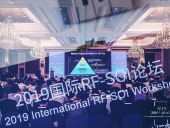
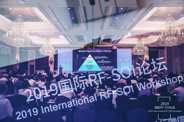
The SOI Consortium’s China 2019 event ran for two days, and it’s taken four (!) posts to cover all the presentations. In this final post we cover the afternoon RF-SOI sessions, which were dedicated to the China RF-SOI ecosystem and the RF value chain. In case you missed them, our previous posts recapped: 1. major keynotes from both the FD-SOI and RF-SOI days; 2. the FD-SOI presentations; 3. the morning sessions of the RF-SOI day; and 4. (this post) the RF-SOI day afternoon sessions. As we noted in Part 1 of our RF-SOI coverage, there were over 500 attendees for the RF-SOI day. And impressively, the room was still packed right through to the very end of the afternoon. Read on! SESSION 2: CHINA RF-SOI ECOSYSTEMSuzhou HunterSun Electronics: Super Opportunity for Integrated RFFE (“Jacky” Yujun Ding, COO)This talk had two parts. First, how is 5G changing the world, and second, what are the RFFE opportunities? He cited IHS data indicating that 5G will create tens of millions of jobs. New products include NB IoT, cellular V2X, as well as traditional PC/tablets and smart phones. But you still need to cover 2/3/4G with 5G. Major growth will happen in 2025-27. In terms of opportunities for RFFE, you've currently got 550mm2 going for $8; in 5G, you'll need 600mm2, but it will cost $16. You need RFSOI for filters and antenna switches, which are in high demand. Parts of the supply chain have no China players. Revenue for BAW is higher than SAW, but there's more SAW. He sees the industry moving heavily into integrated FEM (versus chip-on-board). He finished by itemizing different parts of the RFFE, indicating where the opportunities are (citing some data from Yole), with a special emphasis on integrated products for Chinese companies, with continued investor confidence. SmarterMicro: RF-SOI: Key Technology of Smart Connection (Yangyang Pen, Director) RF-SOI is an enabler of smart connections. However he sees GaAs as better for power, so SmarterMicro has a solution combining RF-SOI and GaAs. They've developed the world's first mMTC RFFE for high-performance upgrades on a single die and software reconfigurable. He notes that for IoT, lifetimes will be longer than 10 years, and that terminals are becoming more powerful. CanaanTek: Critical SOI CMOS Blocks in the 5G NR Sub-6GHz RF Front-End Architectures (Wayne Ni, CTO Board Chairman) CanaanTek is a fabless company working in consumer markets, with switches, tuners and LNAs in SOI-CMOS. He wants to capture 10% of the market with a focus on sub-6. The antenna/tuner is a must, and they've developed solutions for switches here. The figure of merit is RonCoff. He showed a product roadmap on SOI-CMOS. Xpeedic: Innovative EDA Solutions to Enable Differentiated RF-SOI Designs (Feng Ling, CEO)RF-SOI is growing, but there are still design challenges in process, models, filters and packaging. To design a good front end, you need better models and filters. People think passives are easy, but you need accurate models here. Xpeedic has developed design flows that include the effects of packaging early in design. Their products include IRIS, iModeler and Metis (for packaging). They've also introduced substrate modeling in partnership with CWS in France. The product is called SiPEX: it can address linearity in switch or PA designs. You need accurate substrate models to do this. Customers indicate they're seeing big improvements as well as reductions of 25% in chip area. IDP filters is another place they're working, to provide RF filters to fabless IC or module companies. No single filter technology can fit all the needs – IDP is one of them, so they have a broad portfolio of IDP filter technologies. He closed by saying that especially in China, the SOI ecosystem is really growing. SESSION 3: RF VALUE CHAINTowerJazz: Specialized RFSOI Foundry Technology to Support Rapid New Product Development (Paul Hurwitz, Director of RF Technology Development)This presentation gave a full overview of what TowerJazz offers in terms of RF-SOI foundry services with its fabs in Isreal, the US and Japan. What's new in 2019 is a diversifying of 200mm and 300mm. 200mm is best for power handling (for infrastructure/basestation antenna tuners and switch power handling, for example). 300mm is best for SW and LNA integration and higher digital densities. They've got new SOI models for the latest technology generations, and physics-based modeling of RF breakdown for accuracy. With more die being flipped, they needed new substrate modeling. For LNA and switch integration in 300mm, they invested in RF modeling. They also have an in-house MPW (multi-project wafer) program. He noted that customers in China are moving quickly in response to their customer requirements. Okmetic: Tailored Silicon Substrates for RF Applications (Atte Haapalinna, CTO)Okmetic Oy is a niche player in the substrate materials market, with specialties in sensors and MEMS, where they are the market leader. Now part of China’s NSIG group, they are expanding their manufacturing facility in Finland. In this presentation, their CTO talked about their current offerings as well as what they have under development. They do 150-200mm wafers, with a special emphasis on thick SOI. In terms of silicon substrates for RF, ultra-high resistivity is key. Their wafers are also used in IDP – integrated passive devices – for RF and acoustic filters. They are continually improving their high resistivity Magnetic Czochralski (MCz) silicon wafers, and are developing substrates for RF passives for automotive V2X. For RF beyond 6 GHz, they are looking at customized high resistivity silicon wafers for mmWave with researchers and customers. For sensors, they do SOI wafers with built-in cavities. Incize: RF SOI Ecosystem – History Challenges (Mostafa Emam, CEO)The world is exceeding expectations in terms of data usage. While the CAGR for devices is 27%, for data it’s 46%. Therefore each device needs to be faster and more power efficient. Incize recognizes RF as an art, with each piece hand crafted. But artists need to see the whole picture: at Incize, they help 17 companies – including wafer suppliers, foundries and fabless – see that big picture, especially in measurement, characterization and modeling for RF. For wafer suppliers, they do very high-power and very precise on-wafer testing to determine things like intermodulation distortion and substrate interference. For foundries, their specialty is in RF switches, for whom they do harmonics testing and thermal noise management. With those insights, Incize foundry customers have drastically increased the performance of the RF chips they’re manufacturing on trap-rich, high-resistivity SOI wafers. Meanwhile, Incize is also preparing PDKs for future potential substrate generations including GaN-on-Silicon, silicon-on-porous, and new contactless testing techniques for piezoelectric-on-insulator (POI – used in filters in 4/5G). “There’s a really big business opportunity for RF-SOI,” concluded Emam, “and room for everyone.” Cadence: SOI Technology in Intelligent and IoT/Vision/AI Systems (Jonathan Smith, Senior Director)Cadence does SOI enablement at advanced nodes. Smith shared three recent success stories. First, there’s the Musca-S1 test chip they did with Arm, Samsung and Sondrel this past spring. Second, there’s the Tensilica DSP for automotive vision on GlobalFoundries’ 22FDX, which uses 1/10th of the power of existing solutions and was demonstrated at CES. And finally there’s the i.MX line from NXP. In recent news, there’s a new version (18.1) of Virtuoso RF. Though it’s been on the market for 30 years, they’ve added advanced methodologies so that system design and analysis are on the same platform. They’ve also announced National Instruments’ analysis solver, the Clarity 3D solver for next-gen 3D solutions, the integration of multiple electromagnetic (EM) solvers, and advance SiP options. Silvaco: Xena-IP Management Infrastructure for the SOI Ecosystem (Babak Taheri, CEO)Every multi-core SoC today has as many as 200 IPs, if not more. How do you manage that? Tracking and traceability of IP is complicated but important. For IP providers, how do they track where its being used? And for IP consumers, they need to know what they’ve used and where. What’s required is an IP management system to keep track of the different functions and different concerns. Today’s tracking systems don’t talk to each other. Silvaco’s Xena IP management solution organizes all IP data, accounts, products, contracts, devices, support, compliance and reporting. For compliance in particular, they do IP “fingerprinting” and “DNA analysis”, which they’ve patented. The fingerprint is a digital representation of the IP: it’s not just software. It is secure, and can’t be reverse engineered. It’s not a tag: a tag is inserted into the IP, whereas fingerprints are extracted. DNA analysis flags discrepancies and quickly identifies where they are and which files to look in. Xena works in the cloud, enterprise systems or hybrids. The SOI ecosystem will be hearing a lot more about this. ~~ Please note that the China event presentations are all available on our website to anyone whose company or organization is a member of the SOI Consortium.
Read More
The SOI Consortium’s next annual event in Japan takes place on the 30th and 31st of October in Yokohama. Both days of the SOI Design Symposium will take place in the Yokohama Landmark Tower. The event is complimentary, however pre-registration is required – just follow the link here. Rest assured that in addition to the excellent program, the agenda provides ample time for networking.Wednesday, October 30 -- RF and ULP on SOI: IP ProductsOctober 30th showcases industry leaders with ULP IoT applications by NXP, and opportunities in the RF space by STMicroelectronics and Toshiba. The strong development of the design and EDA platform is discussed by ARM, Silvaco, Attopsemi and Dolphin. GlobalFoundries will present on their predictive reliability platform for RF, while Incize discusses the criticality of RF characterization and Secure-IC addresses to important topic of IC security.The day finishes with an overview of the SOI ecosystem by the SOI Industry Consortium. (See the full agenda here.)Thursday, October 31st -- SOI Enabling Photonics and Power InnovationWe start the day with two keynotes on High Voltage SOI electronics for automotive by NXP followed by Soitec on engineered substrate solutions. The Silvaco overview on RF modeling and SOI NB-IoT by SITRI promises to be very interesting. Then the day will offer a deep dive into Photonics touching applications with Cisco, foundry offerings with TowerJazz and GlobalFoundries, EDA with Cadence, and advanced SOI Photonic solutions by Leti-CEA. An ecosystem and market outlook by Soitec wraps-up the day. (See the full agenda here.)We look forward to seeing you there!
Read More
Since the beginning of the year, there’s been a steady stream of excellent news around Samsung Foundry’s 28FDS, their highly successful 28nm FD-SOI offering. Let’s take a look at what’s been happening, as things do seem to be accelerating. By way of reminder, they announced the industry’s first eMRAM (embedded MagnetoResistive RAM) testchip tape-out milestone on 28FDS in September 2017 (you can read the press release here) - which was just a year after they had announced mass production of 28FDS process technology.At the end of 2018, Arm announced the industry’s first Embedded MRAM (eMRAM) compiler IP built on Samsung Foundry’s 28FDS process technology. Follow that with this announcement at the beginning of 2019: Soitec Expands Collaboration with Samsung Foundry on FD-SOI Wafer Supply. The two companies announced that Samsung had secured a high-volume supply of FD-SOI technology to meet industry's current and future demands especially in consumer, IoT and automotive applications. In March came two more big announcements. First: Samsung Electronics Starts Commercial Shipment of eMRAM Product Based on 28nm FD-SOI Process. As they noted in the PR, “Samsung’s 28FDS-based eMRAM solution offers unprecedented power and speed advantages with lower cost. Since eMRAM does not require an erase cycle before writing data, its writing speed is approximately a thousand times faster than eFlash. Also, eMRAM uses lower voltages than eFlash, and does not consume electric power when in power-off mode, resulting in great power efficiency.”Hard on the heals of that came the news that Arm and Samsung Announce IP Platform including eMRAM for 18nm FD-SOI. At the SOI Consortium’s Silicon Valley Symposium in April, Tim Dry (he’s Samsung’s Director of Foundry Marketing for Edge and End Point), gave a terrific presentation. Entitled Samsung’s FDS with MRAM: Enabling Today’s Innovative Low Power Endpoint Products, it details the company’s FDSOI roadmap for the IoT Endpoint Platform (and yes, you can download in its entirety). Then in May at the big Samsung Foundry Forum in Silicon Valley, Arm, in collaboration with Samsung Foundry, Cadence, and Sondrel, demonstrated the first 28nm FD-SOI eMRAM IoT test chip and development board. The Musca-S1 test chip demonstrates a new choice in SoC design for IoT solutions, said Arm. (Sondrel, btw, is Europe's largest independent IC design consultancy.)In parallel, Cadence announced: Cadence Custom/AMS Flow Certified for Samsung 28nm FD-SOI Process Technology. Especially aimed at digitally-assisted analog designs, what’s new here is that the Cadence custom and analog/mixed-signal IC design flow is now Samsung Foundry certified for 28FDS. Samsung’s 28FDS PDK techfile is Mixed-Signal OpenAccess ready, enabling customers to deploy OpenAccess-integrated, fully interoperable Virtuoso-Innovus implementation flows. For its part, at its Foundry Forum, Samsung unveiled extensions of the company’s FD-SOI (FDS) process and eMRAM together with an expanded set of state-of-the-art package solutions. They indicated that the development of the successor to the 28FDS process, 18FDS, and eMRAM with 1Gb capacity will be finished this year.And finally, companies like NXP are shipping exciting new products fabbed on Samsung’s 28FDS. Ron Martino, VP GM of NXP’s i.MX Application Processor Product Line covered key products in his presentation at the SOI Consortium’s Silicon Valley Symposium (see our coverage here). Among them: the i.MX7ULP for long battery life with 2D 3D graphics for wearables and portables in consumer and industrial applications; the i.MX 8 and 8X subsystems for automotive and industrial applications; and the i.MX RT series of “cross-over” processors. The i.MX RT ULP (real-time, ultra-low-power) series, which Martino says is the “new normal”, deals with a high number of sensor inputs. The i.MX RT 1100 MCUs, which have been qualified for automotive and industrial applications, are breaking the gigahertz performance barrier.In July, linuxgizmos.com reported that, “In June, NXP began volume shipments of its super power-efficient i.MX7 ULP, which it announced in 2017. The SoC is billed as the most power-efficient processor on the market that also includes a 3D GPU. […] the ULP version includes a 3D graphics capable Vivante GC7000.” (Vivante, btw, is a VeriSilicon company, which is an SOI Consortium member and a leading proponent of FD-SOI design and IP in China and worldwide.) This is leading to some really nice wins for NXP. For example, they’ve got Amazon's Alexa Voice Service (AVS) leveraging the i.MX RT crossover processor, enabling developers to quickly and easily add Alexa voice assistant capabilities to their products. The RT series has rapidly been expanded, with versions for voice-controlled devices and offline face and expression recognition capabilities for smart home, commercial and industrial devices.Also announced this summer: NXP and Microsoft Bring Microsoft Azure Sphere Security to the Intelligent Edge with a New Energy-Efficient Processor. That collaboration includes development of a new crossover applications processor in NXP’s i.MX 8 series integrating Microsoft’s Azure Sphere security architecture and Pluton Security Subsystem. Their customers “will be able to harness the high-performance and energy efficiency of NXP’s i.MX 8 applications processors combined with Microsoft’s unequaled security and assurance provided by Azure Sphere certified chips”. As Martino concluded in his presentation, “The future of embedded processing [is] enabled by FD-SOI.” And Samsung Foundry’s FD-SOI offerings are clearly a massive enabler of that future.
Read More
Join us! In partnership with our members, the SOI Consortium is co-organizing and participating in two key SOI events coming up in China over the next few weeks. On May 18th, we’ve put together an SOI Forum at the World Semiconductor Congress (WCS) in Nanjing. And on May 23rd 24th, we’ve teamed up with our members SIMIT, Sitri and Leti for another in our series of SOI Academies, including an FD-SOI Training Day. (The last one this past winter was a terrific success – read about that here if you missed our coverage at the time.) QR code for WCS, Nanjing '19At WCS, the SOI Forum (sub-forum #8) is part of the afternoon Innovation Summit. We’ll cover the broader SOI ecosystem, including both RF-SOI and FD-SOI – from wafers to design through manufacturing. Presentations will be given by members of the SOI Consortium team, and by leaders from our membership, including Simgui, NXP, Incize, ST, IBM, Cadence and Xpeedic. Click here or scan the QR code for the full program and registration information. Also at WCS, SOI Consortium member VeriSilicon will be participating in a morning session on AI and IoT Wireless Communications (sub-forum #4). They’ll be giving a presentation on their low-power Bluetooth design platform for GlobalFoundries 22FDX, and their CEO Wayne Dai will be moderating a round-table discussion. You can get more information on that (in Chinese only, tho) here, or follow VeriSilicon on WeChat. QR code for SOI Academy and FD-SOI Training, Shanghaid 2019The SOI Academy in Shanghai is an opportunity for experienced designers to gain solid expertise in FD-SOI. The event begins in the afternoon of May 23rd with a series of informative plenary talks by members of the SOI Consortium team, and by experts from our members Leti, Soitec, VeriSilicon, GlobalFoundries and NXP. The FD-SOI Training starts the next morning, on May 24th.. This is a hands-on event lead by top experts from Leti. The morning is devoted to digital design in FD-SOI, and the afternoon to RF design (including for 5G) in FD-SOI. Attendees will get a comprehensive understanding of design techniques for low-power chips leveraging the multiple benefits and flexibility of FD-SOI technology. Get more information here, or from the WeChat QR code.We've got a busy schedule! To keep up to date with where we and our members will be promoting the SOI ecosystem, be sure to check our Events page regularly.
Read More
Intento Design is working with STMicroelectronics to bring ID-XploreTM EDA software, which is aimed at solving the critical analog design challenges, to FD-SOI process nodes. “ID-Xplore is a disruptive EDA software that accelerates analog design and migration processes by at least one order of magnitude. It reduces the cost and latency inherent to analog design. Currently, there is no similar EDA tool on the market covering the analog design challenges like ID-Xplore,” noted Dr. Ramy Iskander, CEO of Intento Design (see the press release here). ST's FD-SOI design expertise roots, of course, are as deep as they get. “ST’s decision to work with us confirms the relevance of our solution. We are very excited to work jointly with ST teams to take the most benefit out of FD-SOI technology leveraging ST’s pioneering leadership in this area,” continued Dr. Iskander. “We’ve already seen the benefits of ID-Xplore in accelerating the design phase of different analog circuits, thanks to the software’s fast and accurate exploration capabilities in advanced FD-SOI processes,” said Thierry Bion, ST's Hardware Design Director, Aerospace Defense Legacy Division. “By facilitating IP reuse and sharing of design insights between engineers, ID-Xplore™ is helping our teams significantly accelerate new product introductions.” ID-Xplore uses the OpenAccess database standard and is fully integrated within the Cadence design environment. The designer’s implicit and explicit knowledge is expressed as technology-independent constraints, bringing the designers back to their core expertise and creativity. If you want to learn more, the folks over at semiwiki.com have made a number of posts on Intento Design recently. They're really helpful in understanding what the company does, how and why: CEO Interview: Ramy Iskander of Intento Design Edit (by Daniel Nenni) – good backgrounder on the company and product. The Intention View: Disruptive Innovation for Analog Design Edit (by Daniel Nenni) – an excellent interview with Dr. Caitlin Brandon about how the tool works and how it aligns with and supports the way analog designers work. A New Kind of Analog EDA Company Edit (by Daniel Payne) – Daniel Payne started his career as a circuit designer at Intel, and is now a well-known consultant/expert in the EDA world. Here he explores how ID-Xplore actually works and its “cool new automation features”.
Read More