downloadGroupGroupnoun_press release_995423_000000 copyGroupnoun_Feed_96767_000000Group 19noun_pictures_1817522_000000Member company iconResource item iconStore item iconGroup 19Group 19noun_Photo_2085192_000000 Copynoun_presentation_2096081_000000Group 19Group Copy 7noun_webinar_692730_000000Path
Skip to main content
Default Banner Image

storage

As monolithic scaling slows down, the semiconductor industry is increasingly relying on advanced packaging technologies to extend Moore’s law through heterogeneous integration. Higher on-package bandwidth, improved yield resiliency and the need to integrate diverse IP from multiple foundries are driving demand for advanced packaging technologies that address these issues but introduce challenges of their own such as efficient power delivery to all the different domains in a heterogeneous system. SEMI spoke with Kaladhar Radhakrishnan, Intel Fellow at Intel, about heterogeneous system integration trends and new developments in the semiconductor industry. Radhakrishnan shared his views ahead of his keynote at the SEMI Connecting Heterogeneous Systems Summit, 1-3 September 2021, an online event. Join the summit to meet experts from Intel and other key industry influencers. Registration is open. SEMI: What is driving the adoption of electronics and semiconductor devices nowadays and why is the development of new and innovative technologies important? Radhakrishnan: We are living in an increasingly data-driven world where devices have become an integral part of our lives. A recent study estimated that in the United States alone, 13.6 connected devices per capita consume an average of 300 gigabytes worth of data every month. In the workplace, COVID-19 has driven fundamental business changes that has sped up the adoption of digital technologies such as virtual conferencing, remote work, and e-commerce. Organizations are realizing that a high-quality video conference can be an adequate substitute for many in-person meetings. As a result, businesses are accelerating the digital transformation in order to adapt and thrive in this new environment. Five decades of sustained exponential growth in semiconductor performance has conditioned the average digital consumer to expect more from their devices. However, there are some headwinds ahead as traditional scaling slows down and power density rises. Because consumers and businesses are now generating data at a faster rate than they can consume it, technologists need to scale compute, storage, and bandwidth even faster to keep pace. Without investments in research and development of new and innovative technologies to address these challenges, the full potential of this data will go unrealized. SEMI: What forces are heightening the importance of heterogeneous system integration? What are the implications for increased on-package bandwidth, improved yield resiliency and the need to integrate diverse IP from multiple foundries? Radhakrishnan: The semiconductor industry increased transistor density and scaled performance through classical Dennard scaling until the turn of the century. By then, the gate oxide thickness had scaled down to atomic dimensions and the exponential increase in sub-threshold leakage signaled the end of scaling through traditional methods. Since that time, the chip industry has been relying on innovations in transistor materials and structures such as high-k metal gate, strained silicon, and FinFETs to keep pace with Moore’s law. However, this alone will not be sufficient to continue scaling and the industry needs to explore other vectors to augment improvements in transistor technology. Heterogeneous integration through advanced packaging is one key technology that can help drive these gains. Technologies like Foveros can enable device density scaling by creating a 3D stack of multiple die using high-density interconnects. Heterogeneous integration enables chipmakers to move from a monolithic system designed on a single large chip to a heterogeneous system comprised of a number of smaller chiplets. The main benefit of using smaller chiplets is that they improve yield and enable application based customization of the foundry processes. However, if the disaggregation to smaller chiplets is not accompanied by an increase in on-package bandwidth, the power and performance penalties associated with chiplet-to-chiplet communication will hobble system performance. This is why advanced packaging technologies that improve die-to-die communication are key enablers for heterogeneous integration. SEMI: What are some of the key technology challenges in developing heterogeneous systems? Radhakrishnan: The obvious challenge that most people focus on is the need for improved on-package bandwidth. However, as we rely on 3D stacking to continue device scaling at the package level, it is important to comprehend power delivery and thermal challenges as well. Power to the top die has to be delivered through TSVs on the bottom die, which not only adds resistance but also reduces the useful area available on the bottom die. This problem is further exacerbated when we stack more than two die. Excessive noise on the power delivery network can cause timing issues that limit the maximum operating frequency of the transistor. Similarly, when we stack multiple die, we must take into account associated thermal challenges. For example, each interface of the multi-die stack adds thermal resistance, which makes it harder to cool the chips at the bottom. SEMI: What are some of the key global market trends that driving demand for heterogeneous and system-level integration? Radhakrishnan: The number of artificial intelligence (AI) and machine learning applications have grown dramatically due to their ability to solve highly complex problems across a wide range of segments. AI and machine learning models require more memory bandwidth and compute capabilities that are difficult to achieve without some form of heterogeneous integration. Another market trend driving demand for heterogeneous integration is the increasing reliance on custom hardware accelerators. To combat the slowdown in frequency scaling and single-core performance, we have moved to multi-core architectures by tackling the inherent parallelism in our workloads. However, Amdahl’s law tells us that such an approach will hit a bottleneck when we reach the limits of the serial portion of the workload. As these constraints slow the performance of general-purpose processors, the reliance on custom hardware accelerators to boost performance for specific workloads is growing. Heterogeneous integration at the system level with a combination of CPUs, GPUs, FPGAs and other accelerators can optimize system power and performance. SEMI: What solutions is Intel developing to address these market needs? Radhakrishnan: Intel is actively involved in the development of the industry ecosystem for heterogeneous integration. We have developed a number of innovative advanced packaging solutions such as the EMIB and Foveros that are used in products today. Intel is also developing the next generation of advanced packaging technologies, Foveros Omni and Foveros Direct, which will dramatically scale the IO density by using direct Cu-Cu bonding technology. Foveros Omni is a crucial building block technology to enable high-voltage power conversion on the package for efficient power delivery. Intel is uniquely positioned to predict the design needs for future systems and deploy its resources to develop the technology building blocks needed to continue performance scaling. Our IDM 2.0 strategy enables us to leverage our leadership in packaging technologies to design the best products and use the best IP to deliver leading products across a broad range of categories. SEMI: What do you expect from your participation at SEMI Connecting Heterogeneous Systems Summit? Radhakrishnan: I’m hoping to shed some light on some of the new technologies we have been developing at Intel to enable heterogeneous system integration. I also want to bring awareness to the power-related challenges we are facing with heterogeneous systems. I also look forward to listening to what other industry leaders have to say on the topic. Kaladhar Radhakrishnan is an Intel Fellow and a Power Delivery Architect with the Technology Development group at Intel. He plays a significant role in shaping and driving power delivery technologies for Intel microprocessors. His areas of expertise include integrated voltage regulators, advanced packaging and passives technologies. Kaladhar is a two-time recipient of the Intel Achievement Award, the highest Intel honor an individual or small team can receive. He has authored four book chapters, over 40 technical papers in peer-reviewed journals, and has been awarded 35 U.S. patents. He has also served as an adjunct professor at Arizona State University. Kaladhar joined Intel in 2000 soon after receiving his Ph.D. in Electrical Engineering from the University of Illinois at Urbana-Champaign. Serena Brischetto is senior manager of marketing and communications at SEMI Europe.
Read More
In the span of a few short months earlier this year, Mentor Graphics became Siemens EDA and introduced a suite of integrated hardware-assisted verification tools, the first product launch under the new Siemens EDA brand. Jean-Marie Brunet, senior director of marketing, product management and product engineering at Siemens EDA, orchestrated the launch and connected with me for a discussion about the chip design verification space. As he pointed out, verification and validation of systems is a fast-growing and important market segment to the electronic system design ecosystem. Smith: What trends do you see in chip design? What is driving these trends? Brunet: Chip verification costs continue to grow faster than design costs because of factors such as increasing design complexity, rising computing power, surging I/O traffic activity, increasing energy consumption and the widespread use of peripherals. These dynamics are being driven by new data center networking, communications/5G, autonomous driving, artificial intelligence (AI) and machine learning (ML), and storage applications. These trends also indicate the need for more powerful verification tools and expanded verification objectives that include power and performance analysis. Hardware-assisted verification tools are perfect for meeting these demands. Smith: Chip design verification consumes the most time in a project cycle. Why is this so? 
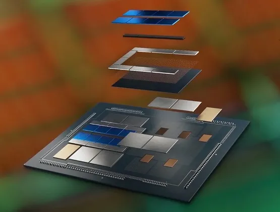
Brunet: The verification of designs reaching multi-billion gates and supported by voluminous software stacks is fraught with challenges. To exhaustively check every possible state in a billion-gate design with simulation alone would require up to trillions of verification cycles. That’s why hardware-assisted verification is one of the fastest-growing technologies in EDA. Given the complexity of today’s SoC design, it’s no surprise that verification is the largest undertaking in the entire project design cycle, consuming more than 50% of it. It also has the greatest impact on quality, cost and schedule because it prevents designs from failing at first silicon. While a respin of a large design taped out at a node below 10 nanometers could cost more than $10 million, delaying delivery of a new product for a few months in a highly competitive market may cost hundreds of millions of dollars. Smith: What other challenges do engineers face trying to verify a chip design will work as intended? Brunet: Verifying an SoC design is a massive undertaking and, in parallel, verification teams are trying to streamline and optimize verification cycles. SoC design groups are tasked with completing full system-level verification prior to creating production masks by thoroughly vetting all hardware blocks, interactions between those blocks, and the software developed for the end application before the chip is built. To alleviate this enormous pressure, they are starting to adopt a shift-left methodology for early functional verification as soon as individual blocks of a SoC design become available. It helps jump-start embedded software validation before full system validation is completed to save time and allow engineers to work in parallel, not serially. While it is an effective approach, it creates the need for a complete and integrated suite of hardware-assisted verification tools to verify and validate a design’s hardware and software components. Smith: How do you define hardware-assisted verification and how does it help solve these challenges? Brunet: A typical definition of hardware-assisted verification is special purpose hardware to accelerate verification. In other words, hardware emulation and FPGA prototyping. Hardware-assisted verification is a mandatory investment as single-die or multi-die chips get larger with more complexity and more interfaces, making hardware and software code integration critical early in the design cycle. Because software performance defines a chip’s success, the need to perform software workload-based analysis is acute, not just analysis of chip functionality, but also accurate performance and power consumption in the context of real-world applications. Hardware-assisted verification is the only option when hardware and software meet. By combining emulation, desktop FPGA prototyping boards and enterprise FPGA prototyping platforms to work on the same SoC design, a verification group can assemble a complete hardware-assisted verification system for thorough and exhaustive verification and validation. Smith: Where are the big opportunities for hardware-assisted verification? Brunet: New end-user applications are coming from computing and storage, AI/ML, 5G, networking and automotive. Recently released market data from the ESD Alliance shows that in 2020, hardware-assisted verification revenues exceeded $700 million. It is reasonable to assume that revenues of $1 billion will be within reach in the next few years given the amount of chip design activity at advanced nodes below 10nm. Smith: With the design/verification and manufacturing phases of the semiconductor supply chain more closely aligning, what role does hardware-assisted verification play? Brunet: Semiconductor manufacturing and the supply chain that supports it benefits greatly from the continued innovation in verification and validation tools and methodologies. With this innovation, designs are delivered to the manufacturing flow with a much greater chance of passing first silicon with success. This reduces friction in the semiconductor supply chain since IP and chips are available when anticipated. Hardware-assisted verification is a quick-moving, highly leveraged resource that helps a design and verification team to ensure chips are manufacturable and meet the functionality, power and performance requirements for the end-product application. Jean-Marie Brunet is the senior director of product management and engineering for the Scalable Verification Solutions Division at Siemens EDA. He has served for over 20 years in application engineering, marketing, and management roles in the EDA industry, and has held IC design and design management positions at STMicroelectronics, Cadence, and Micron, among other companies. Jean-Marie holds a Master's degree in Electrical Engineering from I.S.E.N Electronic Engineering School in Lille, France. Jean-Marie Brunet can be reached at [email protected]. About Bob Smith Robert (Bob) Smith is executive director of the ESD Alliance, a SEMI Technology Community. He is responsible for the management and operations of the ESD Alliance, an international association of companies providing goods and services throughout the semiconductor design ecosystem.
Read More
SEMI met with Gerald Beyer, program manager at imec, to discuss the co-existence of various 3D interconnect technologies and their need for new materials and integration solutions. The two talked in the runup to his presentation at the Advanced Packaging Conference at SEMICON Europa 2018, 13-16, November 2018, in Munich, Germany. To register for the event, click here. SEMI: Can you confirm this trend towards heterogeneous integration and do you think it will be a long-term development trend?Beyer: We consider heterogeneous integration as a scaling booster for functional partitioning and as a fashion method to create systems, which would not be possible or economical on such as a single chip. As you can apply it to numerous systems, we expect it to stay for the long term.SEMI: What are the new critical challenges for the combination of different technologies into one package?Beyer: When you create a complex system, there is usually more than just one challenge. On one side, you need to be able to design such a system. If you disintegrate a large chip, you need to decide how to reconstruct it, i.e. which function goes into which strata. You would like to do that not manually but with a set of tools supporting the designer. Only recently EDA (Electronic Design Automation) and design houses have started to support this idea.On the technology side, interconnections between some strata of such a reconstructed chip will require small pitch interconnects of the order of 1µm pitch and less. Today, wafer-to-wafer bonding technologies have sufficient overlay margins for 1µm pitch. Wafer-to-wafer bonding technologies, however, have a number of constraints such as equal die size and the necessity to realize chip stacking rather in a fab environment than in a traditional packaging house. Die-to-wafer assembly technologies still need to bridge the gap to deep sub 10µm pitch in terms of alignment and cleanliness.SEMI: What kind of new materials or integration solutions do you expect to be developed? Are you working on it already?Beyer: As explained above, die partitioning requires sub 1µm pitch interconnects. We are investigating fine pitch wafer-to-wafer and die-to-wafer (direct) bonding. For the latter, not only new alignment capabilities but also die cleaning and thin die handling technologies need to be developed. To build a complete system with data processing, memories etc., novel integration schemes such as Flip Chip – Fan Out Wafer Level Packaging with high density 2D and 3D interconnect capabilities are being investigated. These new systems differentiate from current ones by high density Through Package Vias (TPV), Si bridges and sub 2µm line/spacing RDL. The new integration approaches push the materials such Temporary Bond Materials (TBM), Wafer Level UnderFill’s (WLUF), photo patternable polymers for fine Line/Spacings to name a few, to the limits. Hence, development of new materials is a key aspect.SEMI: What trends and developments do you expect in the near future and why would you recommend attending the Advanced Packaging Conference?Beyer: The development and commercialization of products using heterogeneous integration is a big effort drawing on resources from EDA vendors, materials and packaging tool suppliers, OSATs, foundries, memory suppliers and IEDMs and academia alike. The agenda of the Advanced Packaging Conference at SEMICON Europa reflects this diversity and I am looking forward to interesting discussions with all participants. Gerald Beyer has been working in the field of 3D Technologies since 2012 as the technology program manager of the 3D System Integration Program of imec. Prior to this role, he was the interconnect program manager and group leader of BEOL integration. He received a PhD in materials science from Imperial College, London and a MSc from Thames Polytechnic, London.Serena Brischetto is a marketing and communications manager at SEMI Europe.
Read More